

Page 1
AH1883
MICROPOWER, ULTRA-SENSITIVE HALL EFFECT SWITCH
Description
The AH1883 micropower Omnipolar Hall Effect switch IC is
designed for portable and battery powered equipment such
as cellular phones, cordless phones, camcorders, PDA’s, and
portable PC’s. Based on two high sensitivity Hall Effect plat es
and chopper stabilized architecture, the AH1883 provides
reliable solution over the whole operating range.
To support portable and battery powered equipment the
design has been optimized to operate from 1.65V to 3.3V and
consumes 13uW typical with a supply of 1.8V. To minimize
PCB space the AH1883 incudes a push-pull output structure,
therefore does not require an external pull up resistor, and is
packaged in small low profile SOT553 and U-DFN2020-3
packages.
Either North or South pole of sufficient strength will turn the
output on. When the magnetic flux density (B) is larger than
operate (Bop) the output is switched on. The output is turned
off when B becomes lower than the release point (Brp). The
output will remain off when there is no magnetic field.
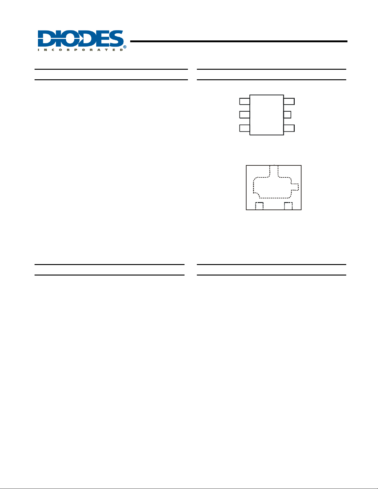
Pin Assignments
NC
GND
NC
(Top View)
1
2
3
1. Vdd
SOT553
(Top View)
3. GND
2. OUT PU T
U-DFN2020-3
5
4
OUTPUT
Vdd
Features
• Micropower operation
• Operation with North or South Pole
• 1.65V to 3.3V battery operation
• Chopper stabilized
o Superior temperature stability
o Extremely Low Switch-Point Drift
o Insensitive to Physical Stress
• Good RF noise immunity
• -40°C to 85°C operating temperature
• ESD (HBM) > 6kV in SOT553 and U-DFN2020-3
• Small low profile packages: SOT553 and U-DFN2020-3
• “Green” Molding Compound
Applications
• Cellular phone
• PDA
• Portable PCs – Netbook, Notebook, Tablets
• Camcorders
• Cordless phone
• Handheld game consoles
• Proximity detection and contact-less switch
applications
AH1883
Document number: DS31296 Rev. 6 - 2
1 of 10
www.diodes.com
September 2011
© Diodes Incorporated
Page 2
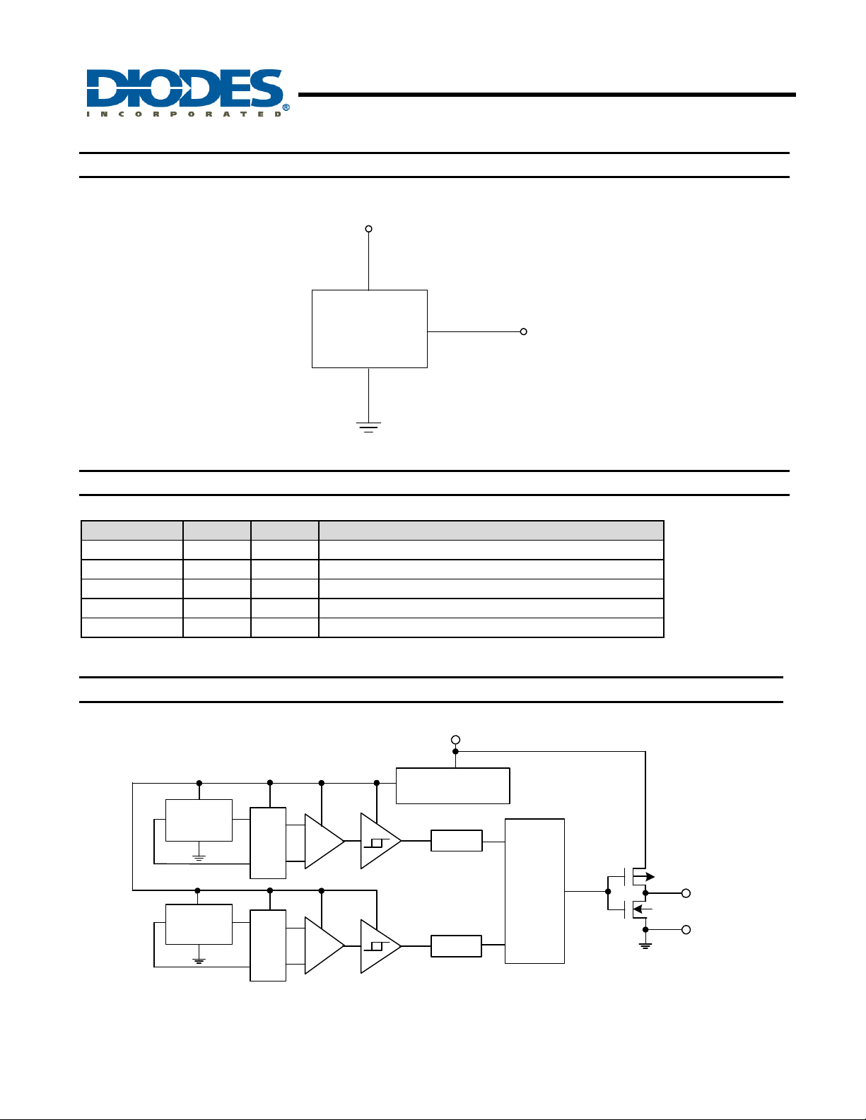
Typical Application Circuit
AH1883
MICROPOWER, ULTRA-SENSITIVE HALL EFFECT SWITCH
Vdd
AH1883
Output
GND
Pin Descriptions
Pin Name P/I/O Pin # Description
NC 1 No Connection
GND P/I 2 Ground
NC 3 No Connection
Vdd P/I 4 Power Supply Voltage
Output O 5 Output Pin ( active Low )
Functional Block Diagram
Vdd
Hall
Plate
Hall
Plate
AH1883
Document number: DS31296 Rev. 6 - 2
Sleep/Awake Logic
Cancellation
Offset
Amp
Cancellation
Offset
Amp
and Power Switch
Latch
Latch
Output
Driver
Controller
Output
GND
2 of 10
www.diodes.com
September 2011
© Diodes Incorporated
Page 3
AH1883
Absolute Maximum Ratings (T
Symbol Characteristics Values Unit
Vdd Supply voltage 5 V
B Magnetic flux density Unlimited
TS
PD
TJ
Notes: 1. Stresses greater than the 'Absolute Maximum Ratings' specified above, may cause permanent damage to the device. These are stress ratings only;
functional operation of the device at these or any other conditions exceeding those indicated in this specification is not implied. Device reliability
may be affected by exposure to absolute maximum rating conditions for extended periods of time
Storage Temperature Range -65 to +150 °C
Package Power Dissipation 230 mW
Maximum Junction Temperature 150 °C
MICROPOWER, ULTRA-SENSITIVE HALL EFFECT SWITCH
= 25°C, Note 1)
A
Recommended Operating Conditions (T
= 25°C)
A
Symbol Parameter Conditions Rating Unit
Vdd Supply Voltage Operating 1.65 to 3.3 V
TA
Operating Temperature Range Operating -40 to +85 °C
Electrical Characteristics (TA = 25°C, Vdd = 1.8V, unless otherwise specified)
Symbol Characteristic Conditions Min Typ. Max Unit
VOH
VOL
Idd(en)
Idd(dis) Chip disable - 5 8 uA
Idd(avg) average supply current - 7 12 uA
Tawake Awake Time - 50 100 µs
Tperiod Period - 50 100 ms
D.C. Duty Cycle - 0.1 - %
Output On Voltage (High side)
Output On Voltage (Low side)
Supply Current
IO= -0.5mA
IO= 0.5mA
Chip enable - 2 4 mA
Vdd-0.2 - - V
- - 0.2 V
AH1883
Document number: DS31296 Rev. 6 - 2
3 of 10
www.diodes.com
September 2011
© Diodes Incorporated
Page 4

AH1883
Magnetic Characteristics (T
Symbol Characteristic Min Typ. Max Unit
Bops(south pole to brand side)
Bopn(north pole to brand side) -55 -37 Brps(south pole to brand side)
Brpn(north pole to brand side) - -29 -6
Bhy(|Bopx|-|Brpx|) Hysteresis 3 8 -
Notes: 2. Typical data is at TA = 25°C, Vdd = 3V, and for design information only.
3. The magnetic characteristics may vary with supply voltage, operating temperature and after soldering.
MICROPOWER, ULTRA-SENSITIVE HALL EFFECT SWITCH
= 25°C, Vdd = 1.8V~3.0V, Note 2 & 3)
A
(1mT=10 Gauss)
Operate Point
Release Point
- 37 55
6 29 -
Gauss
Output
)
dd
B
opn
( off-state )
hy
B
rpn
B
Turn off
V
0
sat
Voltage
Output
(
V
Turn on
( on-state )
( Magnetic flux density B )
Output
)
( off-state )
Voltage
Turn off
Output
(
V
sat
0
B
rps
B
hy
B
( Magnetic flux density B )
V
dd
Turn on
( on-state )
ops
AH1883
Document number: DS31296 Rev. 6 - 2
4 of 10
www.diodes.com
September 2011
© Diodes Incorporated
Page 5

MICROPOWER, ULTRA-SENSITIVE HALL EFFECT SWITCH
Typical Operating Characteristics
AH1883
AH1883 Switch points vs. Temperature (Vdd = 1.8V)
50
40
30
20
10
0
-10
Gauss(G)
-20
-30
-40
-50
-40 -15 10 35 60 85
Temperature (℃)
Idd (avg.)
unit: μA
9
8
7
6
5
4
3
2
1
0
-40 -15 10 35 60 85
AH1883 Idd(avg.) vs. Temperature
Temperature (℃)
Bops
Brps
Bopn
Brpn
Bhy_s
Bhy_n
1.65V
1.8V
3.3V
AH1883 Switch points vs. Vdd (TA =25 ℃)
50
40
30
20
10
0
Gauss(G)
-10
-20
-30
-40
-50
1.65 1.9 2.15 2.4 2.65 2.9 3.15 3.4 3.65 3.9
Vdd(V)
Idd (avg.)
unit: μA
10
9
8
7
6
5
4
3
2
1
0
1.65 1.9 2.15 2.4 2.65 2.9 3.15 3.4 3.65 3.9
A H1883 Idd(avg .) vs. Vd d (TA=25 ºC)
Vdd(V)
Bops
Brps
Bopn
Brpn
Bhy_s
Bhy_n
AH1883
Document number: DS31296 Rev. 6 - 2
5 of 10
www.diodes.com
September 2011
© Diodes Incorporated
Page 6

XX
Performance Characteristics
For SOT553 and U-DFN2020-3
TA (°C)
PD (mW)
25 50 60 70 80 85 90 100 110 120 130 140 150
230 184 166 147 129 120 110 92 74 55 37 18 0
P
(mW )
D
300
200
100
0
0 2 5 50 75 100 125 150
AH1883
MICROPOWER, ULTRA-SENSITIVE HALL EFFECT SWITCH
Power Dissipation Curve
85-40
TA (oC)
Ordering Information
Device
AH1883-ZG-7 Z SOT553 3000/Tape & Reel -7
AH1883-FJG-7 FJ U-DFN2020-3 3000/Tape & Reel -7
Notes: 4. EU Directive 2002/95/EC (RoHS). All applicable RoHS exemptions applied. Please visit our website at
http://www.diodes.com/products/lead_free.html.
5. Pad layout as shown on Diodes Inc. suggested pad layout document AP02001, which can be found on our website at
http://www.diodes.com/datasheets/ap02001.pdf.
Package
Z : SOT553
FJ :
Package
Code
AH 1883 -
U-DFN2020-3
Packaging
(Note 4 & 5)
G -7
Green
G : Green
Quantity Part Number Suffix
Packing
7 : Tape & Reel
7” Tape and Reel
AH1883
Document number: DS31296 Rev. 6 - 2
6 of 10
www.diodes.com
September 2011
© Diodes Incorporated
Page 7

Marking Information
(1) SOT553
(2) U-DFN2020-3
AH1883
MICROPOWER, ULTRA-SENSITIVE HALL EFFECT SWITCH
( Top View )
XX
: Identification Code
Y : Year : 0~9
W
XX Y W X
Part Number Package Identification Code
AH1883 SOT553 KP
: Week : A~Z : 1~26 week;
a~z : 27~52 week;
z represents 52 and 53 week
: Internal code
X
( Top View )
Pin 1 indicator
: Identification C ode
XX
Y
WX
XX
Y : Year : 0~9
W
: Week : A~Z : 1~26 week;
a~z : 27~52 week;
z represents 52 and 53 week
X : In ternal cod e
Part Number Package Identification Code
AH1883 U-DFN2020-3 KP
AH1883
Document number: DS31296 Rev. 6 - 2
7 of 10
www.diodes.com
September 2011
© Diodes Incorporated
Page 8

A
A
MICROPOWER, ULTRA-SENSITIVE HALL EFFECT SWITCH
Package Outline Dimensions (All Dimensions in mm)
(1) Package Type: SOT553
E1
D
e1
e
E
L
b (5 places)
a
A
c
(2) Package Type: U-DFN2020-3
A
A3
SEATING PLANE
Pin#1 ID
A1
D
D2
E
E2
e
L
L
b
SOT553
Dim Min Max Typ
0.55 0.60 0.60
c
0.10 0.18 0.15
D
1.50 1.70 1.60
E
1.55 1.70 1.60
E1
1.10 1.25 1.20
L
0.10 0.30 0.20
b
0.15 0.30 0.20
e
e1
a
0.50 Typ
1.00 Typ
6°
8° 7°
ll Dimensions in mm
U-DFN2020-3
Dim Min Max Typ
A 0.57 0.63 0.60
A1 0 0.05 0.02
A3
⎯ ⎯
b 0.20 0.30 0.25
D 1.95 2.075 2.00
D2 1.10 1.30 1.20
e
⎯ ⎯
E 1.95 2.075 2.00
E2 0.80 1.00 0.90
L 0.35 0.45 0.40
All Dimensions in mm
0.152
0.50
AH1883
AH1883
Document number: DS31296 Rev. 6 - 2
8 of 10
www.diodes.com
September 2011
© Diodes Incorporated
Page 9

Taping Orientation (Note 6)
For U-DFN2020-3
AH1883
MICROPOWER, ULTRA-SENSITIVE HALL EFFECT SWITCH
Notes: 6. The taping orientation of the other package type can be found on our website at http://www.diodes.com/datasheets/ap02007.pdf.
AH1883
Document number: DS31296 Rev. 6 - 2
www.diodes.com
9 of 10
September 2011
© Diodes Incorporated
Page 10

AH1883
MICROPOWER, ULTRA-SENSITIVE HALL EFFECT SWITCH
IMPORTANT NO TICE
DIODES INCORPORATED MAKES NO WARRANTY OF ANY KIND, EXPRESS OR IMPLIED, WITH REGARDS TO THIS
DOCUMENT, INCLUDING, BUT NOT LIMITED TO, THE IMPLIED WARRANTIE S OF MERCHANTABILITY AND FITNESS FOR A
PARTICULAR PURPOSE (AND THEIR EQUIVALENTS UNDER THE LAWS OF ANY JURISDICTION).
Diodes Incorporated and its subsidiaries reserve the right to make modifications, enhancements, improvements, corrections or other
changes without further notice to this document and any product described herein. Diodes Incorporated does not assume any liability
arising out of the application or use of this document or any product described herein; neither does Diodes Incorporated convey any
license under its patent or trademark rights, nor the rights of others. Any Customer or user of this document or products described
herein in such applications shall assume all risks of such use and will agree to hold Diodes Incorporated and all the companies
whose products are represented on Diodes Incorporated website, harmless against all damages.
Diodes Incorporated does not warrant or accept any liability whatsoever in respect of any products purchased through unauthorized
sales channel.
Should Customers purchase or use Diodes Incorporated products for any unintended or unauthorized application, Customers shall
indemnify and hold Diodes Incorporated and its representatives harmless against all claims, damages, expenses, and attorney fees
arising out of, directly or indirectly, any claim of personal injury or death associated with such unintended or unauthorized application.
Products described herein may be covered by one or more United States, international or foreign patents pending. Product names
and markings noted herein may also be covered by one or more United States, international or foreign trademarks.
LIFE SUPPORT
Diodes Incorporated products are specifically not authorized for use as critical components in life support devices or systems without
the express written approval of the Chief Executive Officer of Diodes Incorporated. As used herein:
A. Life support devices or systems are devices or systems which:
1. are intended to implant into the body, or
2. support or sustain life and whose failure to perform when properly used in accordance with instructions for use provided
in the labeling can be reasonably expected to result in significant injury to the user.
B. A critical component is any component in a life support device or system whose failure to perform can be reasonably expected
to cause the failure of the life support device or to affect its safety or effectiveness.
Customers represent that they have all necessary expertise in the safety and regulatory ramifications of their life support devices or
systems, and acknowledge and agree that they are solely responsible for all legal, regulatory and safety-related requirements
concerning their products and any use of Diodes Incorporated products in such safety-critical, life support devices or systems,
notwithstanding any devices- or systems-related information or support that may be provided by Diodes Incorporated. Further,
Customers must fully indemnify Diodes Incorporated and its representatives against any damages arising out of the use of Diodes
Incorporated products in such safety-critical, life support devices or systems.
Copyright © 2011, Diodes Incorporated
www.diodes.com
AH1883
Document number: DS31296 Rev. 6 - 2
10 of 10
www.diodes.com
September 2011
© Diodes Incorporated
 Loading...