

Page 1
AH1822
MICROPOWER OMNIPOLAR HALL-EFFECT SENSOR
SWITCH
Features
• Micropower operation
• Operation with magnetic field of either north or south
pole (omnipolar)
• 2.5V to 5.5V battery operation
• Chopper stabilized
• Superior temperature stability
• Extremely Low Switc h-Point Drift
• Insensitive to Physical Stress
• Good RF noise immunity
• -40°C to 85°C operating temperature
• ESD (HBM) > 5KV
• DFN2015-6 and DFN3020-6: Available in “Green”
Molding Compound (No Br, Sb)
• Lead Free Finish/ RoHS Compliant (Note 1)
Applications
• Cover switch in clam-shell cellular phones
• Cover switch in Notebook PC/PDA
• Contact-less switch in consumer products
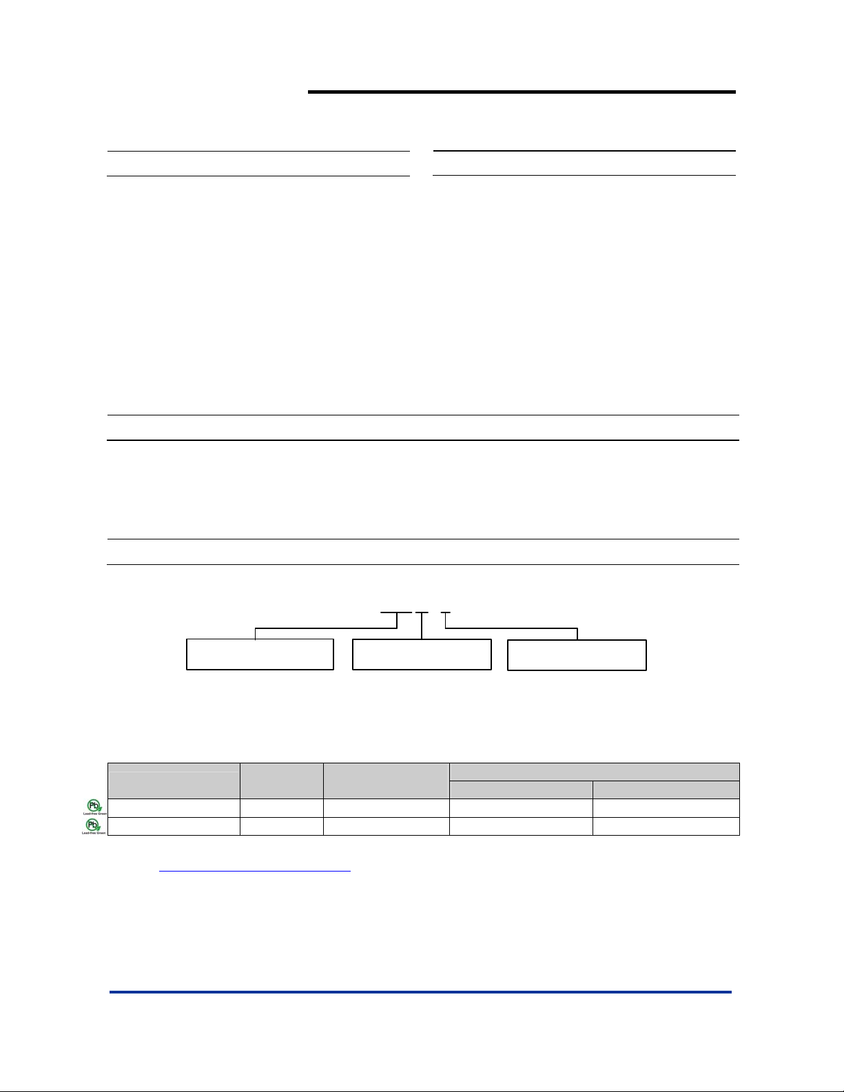
Ordering Information
AH 1822 - XXX G - 7
General Description
AH1822 is comprised of two Hall effect plates and an open-drain
output driver, mainly designed for battery-operation, hand-held
equipment (such as Cellular and Cordless Phone, PDA). The
total power consumption in normal operation is typically 24μW
with a 3V power source.
Either north or south pole of sufficient strength will turn the output
on. The output will be turned off under no magnetic field. While
the magnetic flux density (B) is larger than operating point (Bop),
the output will be turned on (low), the output is held until B is
lower than release point (Brp), then turned off.
Package
FT4 : DFN2015-6
FU4 : DFN3020-6
G : Green
PackingGreen
7 : Tape & Reel
Device
Package
Code
Packaging
(Note 2)
Quantity Part Number Suffix
7” Tape and Reel
AH1822-FT4G-7 FT4 DFN2015H4-6 3000/Tape & Reel -7
AH1822-FU4G-7 FU4 DFN3020H4-6 3000/Tape & Reel -7
Notes: 1. EU Directive 2002/95/EC (RoHS). All applicable RoHS exemptions applied, see EU Directive 2002/95/EC Annex Notes.
2. Pad layout as shown on Diodes Inc. suggested pad layout document AP02001, which can be found on our website at
http://www.diodes.com/datasheets/ap02001.pdf
.
AH1822 Rev. 5 1 of 9 FEBRUARY 2009
www.diodes.com © Diodes Incorporated
Page 2
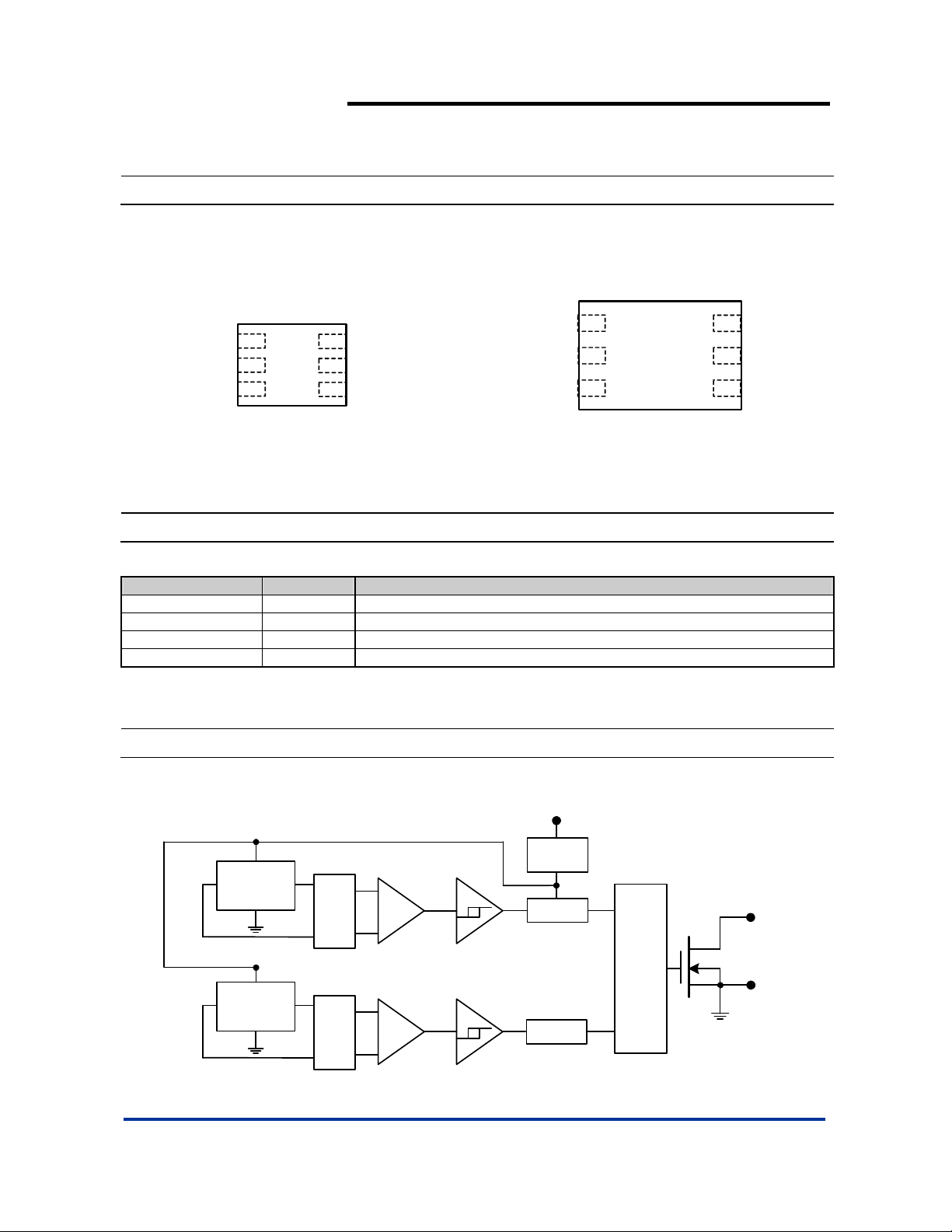
Pin Assignments
( Top View )
1
NC
Vdd
GND
2
3
AH1822
MICROPOWER OMNIPOLAR HALL-EFFECT SENSOR
SWITCH
( Top View )
6
5
4
NC
Output
GND
Output
NC
GND
1
2
3
6
Vdd
5
NC
4
GND
DFN2015-6
Notes: 3. NC is “No Connection” which is recommended to be tied to ground.
Pin Descriptions
Pin Name P/I/O Description
Vdd P/I Power Supply Input
GND P/I Ground
Output O Output Pin
NC NC No Connected
Block Diagram
Vdd
Power
switch
Latch
Hall Plate
Cancelling
Offset
Amp
DFN3020-6
Output
Logical
Hall Plate
AH1822 Rev. 5 2 of 9 FEBRUARY 2009
Cancelling
Offset
Amp
www.diodes.com © Diodes Incorporated
Latch
GND
Page 3
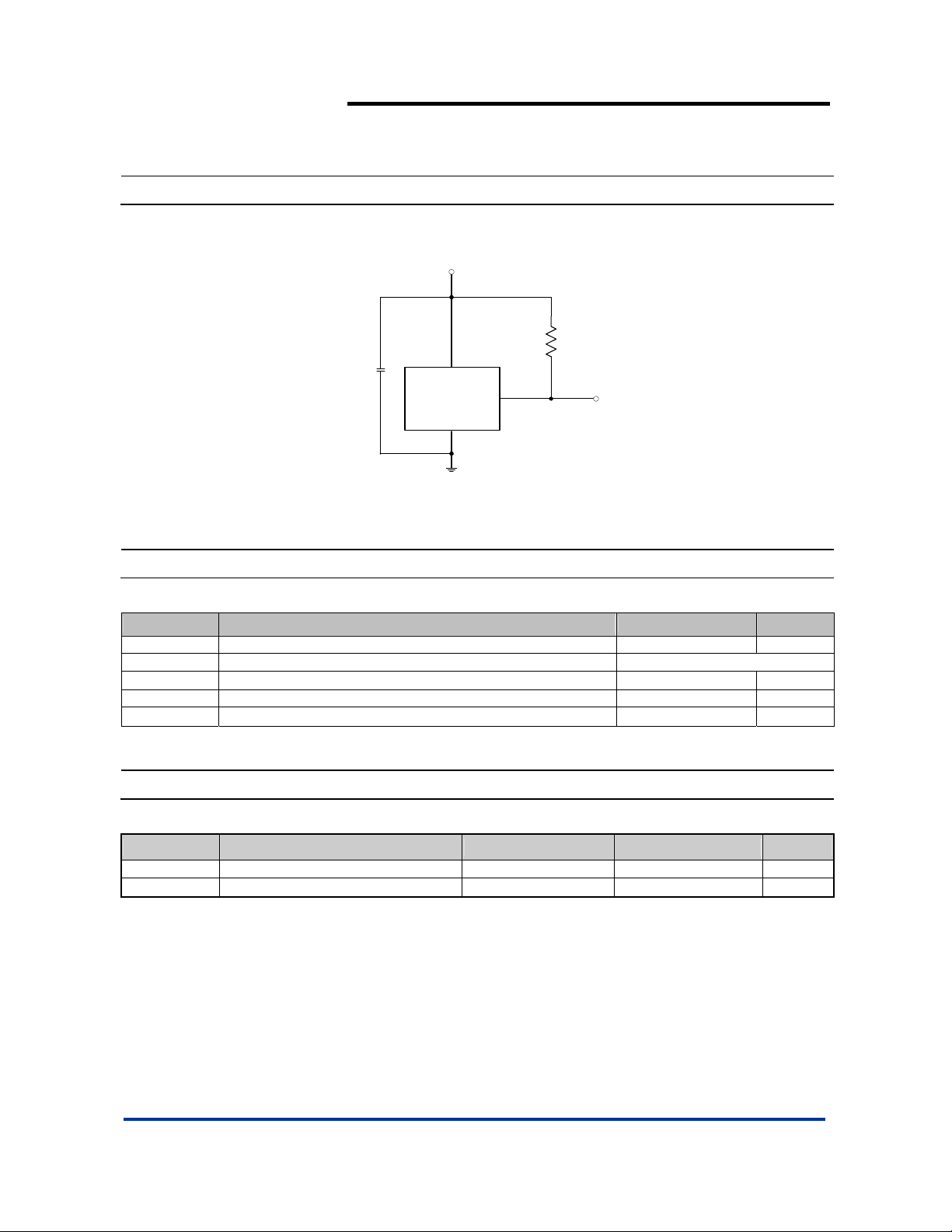
Typical Circuit
AH1822
MICROPOWER OMNIPOLAR HALL-EFFECT SENSOR
SWITCH
2.5~5.5V
R
L
C
AH1822
GND
Notes: 4. C is for power stabilization and to strengthen the noise immunity, the recommended capacitance is 10nF~100nF.
R
is the pull-up resistor, the recommended resistance is 10KΩ~100KΩ.
L
Output
Absolute Maximum Ratings (at TA= 25°C)
Symbol Characteristics Values Unit
Vdd Supply voltage 7 V
B Magnetic flux density Unlimited
TST Storage Temperature Range -65 to +150
PD Package Power Dissipation 230 mW
TJ
Maximum Junction Temperature 150
Recommended Operating Conditions
Symbol Parameter Conditions Rating Unit
Vdd Supply Voltage Operating 2.5~5.5 V
TA Operating Temperature Range Operating -40 to +85
°C
°C
°C
AH1822 Rev. 5 3 of 9 FEBRUARY 2009
www.diodes.com © Diodes Incorporated
Page 4

⎯
⎯
⎯
AH1822
MICROPOWER OMNIPOLAR HALL-EFFECT SENSOR
SWITCH
Electrical Characteristics (TA = +25°C, Vdd = 3V; unless otherwise specified)
Symbol Characteristic Conditions Min Typ. Max Unit
Vout Output On Voltage Iout=1mA
Ioff Output Leakage Current Vout=5.5V, Output off
Idd(en)
Idd(en)
Chip enable , T
Chip enable , T
Vdd = 2.5~5.5V
A= 25°C , Vdd = 3V ⎯
A= -40~85°C ,
⎯
⎯
Idd(dis) Chip disable , TA= 25°C , Vdd = 3V ⎯ 5 10 µA
Idd(dis)
Idd(avg)
Idd(avg)
Supply Current
Chip disable , T
Vdd = 2.5~5.5V
Average supply current ,
A= 25°C , Vdd = 3V
T
Average supply current ,
T
A= -40~85°C , Vdd = 2.5~5.5 V
A= -40~85°C ,
⎯
⎯
⎯
FC Chopping Frequency For design information only
Tawake Awake Time (Note 5)
Tperiod Period (Note 5)
D.C. Duty Cycle
Notes: 5. When power is initially on, the operating Vdd (2.5V to 5.5V) must be applied to be guaranteed for the output sampling. The output state is valid
after the second operating phase (typical 150ms).
0.1 0.3 V
<0.1
3 6 mA
3 10 mA
5 18 µA
8 16 µA
8 28 µA
300
⎯
⎯
⎯
75 150 µs
75 150 ms
0.1
1 µA
KHz
⎯
%
Tperiod
Tawake
Idd(en)
Sample and output
Idd (dis)
0
latched
AH1822 Rev. 5 4 of 9 FEBRUARY 2009
www.diodes.com © Diodes Incorporated
Page 5

MICROPOWER OMNIPOLAR HALL-EFFECT SENSOR
Magnetic Characteristics (TA=25°C, Vdd=3V, Note 6, 7)
Symbol Characteristic Min Typ. Max Unit
Bops(south pole to brand side)
Bopn(north pole to brand side) -55 -28 Brps(south pole to brand side)
Brpn(north pole to brand side) - -20 -10
Bhy( BrpxBopx − )
Notes: 6. Typical data is at Ta = 25°C, Vdd = 3V, and for design information only.
7. Operatin g point and release point will vary with supply voltage and operati ng temperature.
Operate Point
Release Point
Hysteresis 5 8 -
Output
- 28 55
10 20 -
Output
AH1822
SWITCH
(1mT=10 Gauss)
Gauss
( off-state )
Vcc
Turn off
Turn on
Bhy
( Output Voltage )
( on-state )
Bopn Brpn 0
( Magnetic flux density B )
Performance Characteristics
TA (°C)
PD (mW)
25 50 60 70 80 85 90 100 110 120 130 140 150
230 184 166 147 129 120 110 92 74 55 37 18 0
P
(m W)
D
300
200
Turn off
( Output Voltage )
Vsat
Vsat
( Magnetic flux density B )
Power Dissipation Curve
( off-state )
Bhy
Brps Bops0
Vcc
Turn on
( on-state )
100
0
0 25 50 75 100 125 150
85
TA (。C)
AH1822 Rev. 5 5 of 9 FEBRUARY 2009
www.diodes.com © Diodes Incorporated
Page 6

Marking Information
(1) DFN2015-6
( Top View )
Part Number Package Identification Code
AH1822 DFN2015-6 K7
XX
Y
AH1822
MICROPOWER OMNIPOLAR HALL-EFFECT SENSOR
Pin 1 indicator
XX
: Identification Code
WX
Y : Yea r : 0 ~ 9
: Week : A~Z : 1~26 week ;
W
a~z : 27~52 week; z represents
52 and 53 week
: A~Z : G reen
X
SWITCH
(2) DFN3020-6
Part Number Package Identification Code
AH1822 DFN3020-6 K8
( Top View )
X X
XY
W
Pin 1 indicator
XX
: Identific a tion C o d e
Y : Ye a r : 0 ~ 9
: Week : A~Z : 1~26 week;
W
a~z : 27~52 week; z represents
52 and 53 week
X
: A~ Z : Gr een
AH1822 Rev. 5 6 of 9 FEBRUARY 2009
www.diodes.com © Diodes Incorporated
Page 7

MICROPOWER OMNIPOLAR HALL-EFFECT SENSOR
Package Information (All Dimensions in mm)
(1) Package type: DFN2015-6
aaa A
2x-
1.45/1.575
B
1.95/2.075
aaa B
2x-
ccc C
6x-
0.08 C
0.40Max.
(Pin #1)
0/0.05
(Pin #1)
0.25/0.35
1.0/1.2
4x-0.50
A
0.13Typ.
C
0.7/0.9
Seating Plane
4x-0.50
(Pin #1)
2.0
AH1822
SWITCH
6x-0.75
0.20/0.30
Bottom View
C
bbb
AB
6x-0..30
Land Pattern Recommendation
(Unit:mm)
(2) Package type: DFN3020-6
aaa A
2X-
1.95/2.075
6x-
2X-
bbb
aaa
ccc C
0.08 C
B
0.40Typ.
C
AB
B
2.95/3.075
(Pin #1)
0/0.05
(Pin #1 ID)
1.124/1.324
0.50/0.60
0.20/0.30
Bottom View
0.50Typ.
0.942/1.142
A
0.15Typ.
Seating Plane
C
3.0
Land Pattern Recommendation
4x-0.50
(Unit: mm)
6x-0.30
(Pin #1)
4x-0.75
AH1822 Rev. 5 7 of 9 FEBRUARY 2009
www.diodes.com © Diodes Incorporated
Page 8

Taping Orientation
(1) DFN2015-6
AH1822
MICROPOWER OMNIPOLAR HALL-EFFECT SENSOR
SWITCH
(2) DFN3020-6
Notes: 8. The taping orientation of the other package type can be found on our website at http://www.diodes.com/datasheets/ap02007.pdf
AH1822 Rev. 5 8 of 9 FEBRUARY 2009
www.diodes.com © Diodes Incorporated
.
Page 9

AH1822
MICROPOWER OMNIPOLAR HALL-EFFECT SENSOR
SWITCH
IMPORTANT NOTICE
Diodes Incorporated and its subsidiaries reserve the right to make modifications, enhancements, improvements, corrections or other changes without further
notice to any product herein. Diodes Incorporated does not assume any liability arising out of the application or use of any product described herein; neither
does it convey any license under its patent rights, nor the rights of others. The user of products in such applications shall assume all risks of such use and will
agree to hold Diodes Incorporated and all the companies whose products are represented on our website, harmless against all damages.
LIFE SUPPORT
Diodes Incorporated products are not authorized for use as critical components in life support devices or systems without the expressed written approval of the
President of Diodes Incorporated.
AH1822 Rev. 5 9 of 9 FEBRUARY 2009
www.diodes.com © Diodes Incorporated
 Loading...