Diodes AH180N User Manual

A
Description
The AH180N is a high sensitivity, micro power Omnipolar Hall Effect
switch IC designed for portable and battery powered equipment such
as cellular phones, PDA’ s and portable PC’ s. Based on two sensitive
Hall Effect plates and a chopper stabilized architecture the AH180N
provides a reliable solution over the whole operating range. To
support portable and battery powered equipment the design has been
optimized to operate over the supply range of 2.5V to 5.5V and
consumes only 24µA with a supply of 3V.
The single open drain output can switched on with either a North or
South pole of sufficient strength. When the magnetic flux density (B)
is larger than operate point (Bop) the output is switched on (pulled
low). The output is turned off when B becomes lower than the release
point (Brp). The output will remain off when there is no magnetic field.
H180N
MICROPOWER OMNIPOLAR HALL-EFFECT SWITCH
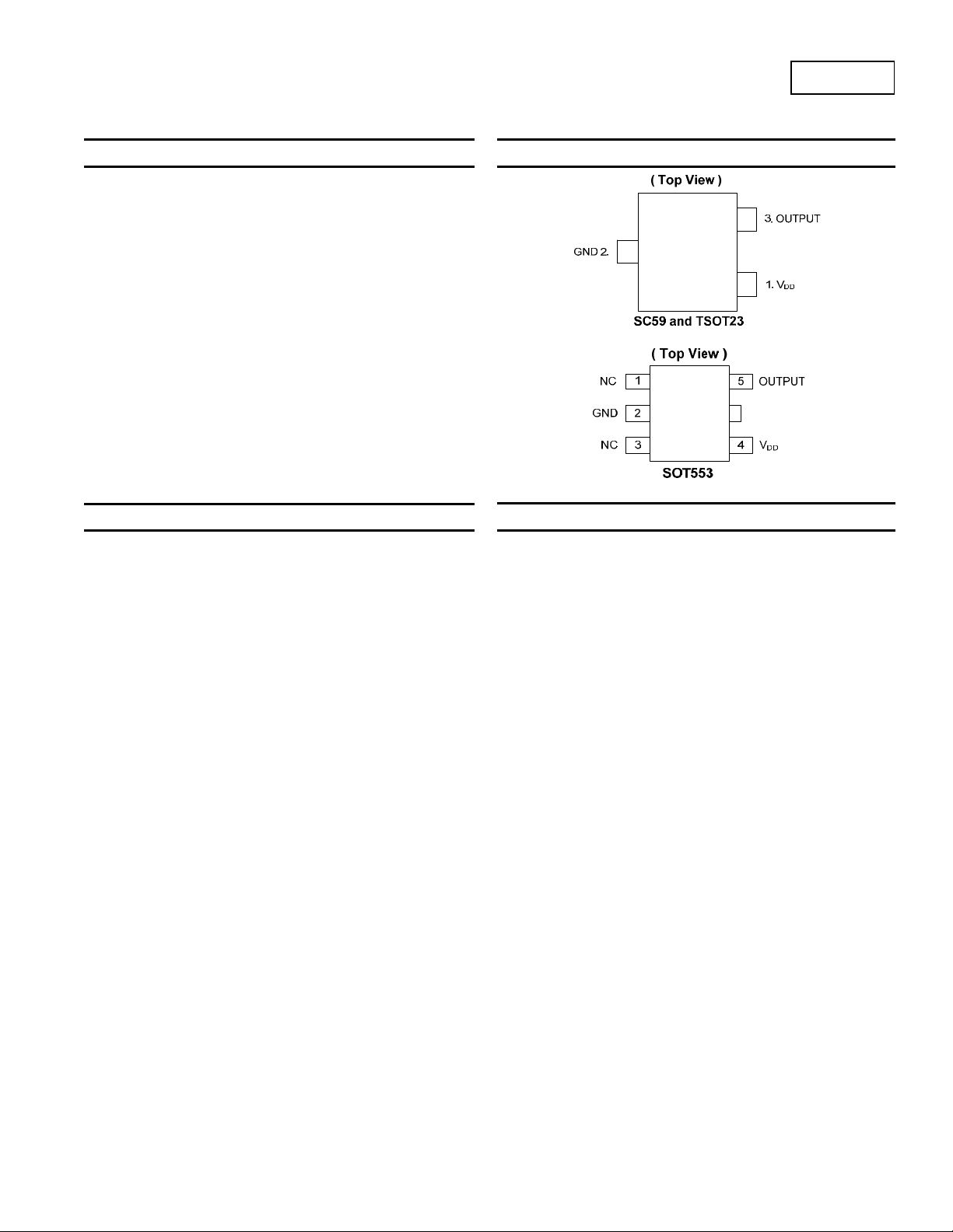
Pin Assignments
Features
• Omnipolar (North or South pole) Operation
• High Sensitivity
• Single Open Drain Output
• Micropower Operation
• 2.5V to 5.5V Operating Range
• Chopper Stabilized Design Provides
Superior Temperature Stability
Minimal Switch Point Drift
Enhanced Immunity to Stress
• Good RF Noise Immunity
• -40°C to +85°C Operating Temperature
• ESD (HBM) > 6KV
• SC59 (SOT23), TSOT23, and SOT553 Low Profile Packages
• Totally Lead-Free & Fully RoHS Compliant (Notes 1 & 2)
• Halogen and Antimony Free. “Green” Device (Note 3)
Notes: 1. No purposely added lead. Fully EU Directive 2002/95/EC (RoHS) & 2011/65/EU (RoHS 2) compliant.
2. See http://www.diodes.com for more information about Diodes Incorporated’s definitions of Halogen- and Antimony-free, "Green" and Lead-free.
3. Halogen- and Antimony-free "Green” products are defined as those which contain <900ppm bromine, <900ppm chlorine (<1500ppm total Br + Cl)
and <1000ppm antimony compounds.
Applications
• Cover Switch in Clam-Shell or Slide Type Cellular Phones
• Display Switch for Portable PCs
• On/Off Switch for PDAs and Digital Cameras
• Contact-Less Switch in Consumer Products
AH180N
Document number: DS32174 Rev. 4 - 2
1 of 8
www.diodes.com
August 2012
© Diodes Incorporated

A
Typical Applications Circuit
C
2.5V to 5.5V
V
DD
AH180N
GND
R
L
OUTPUT
H180N
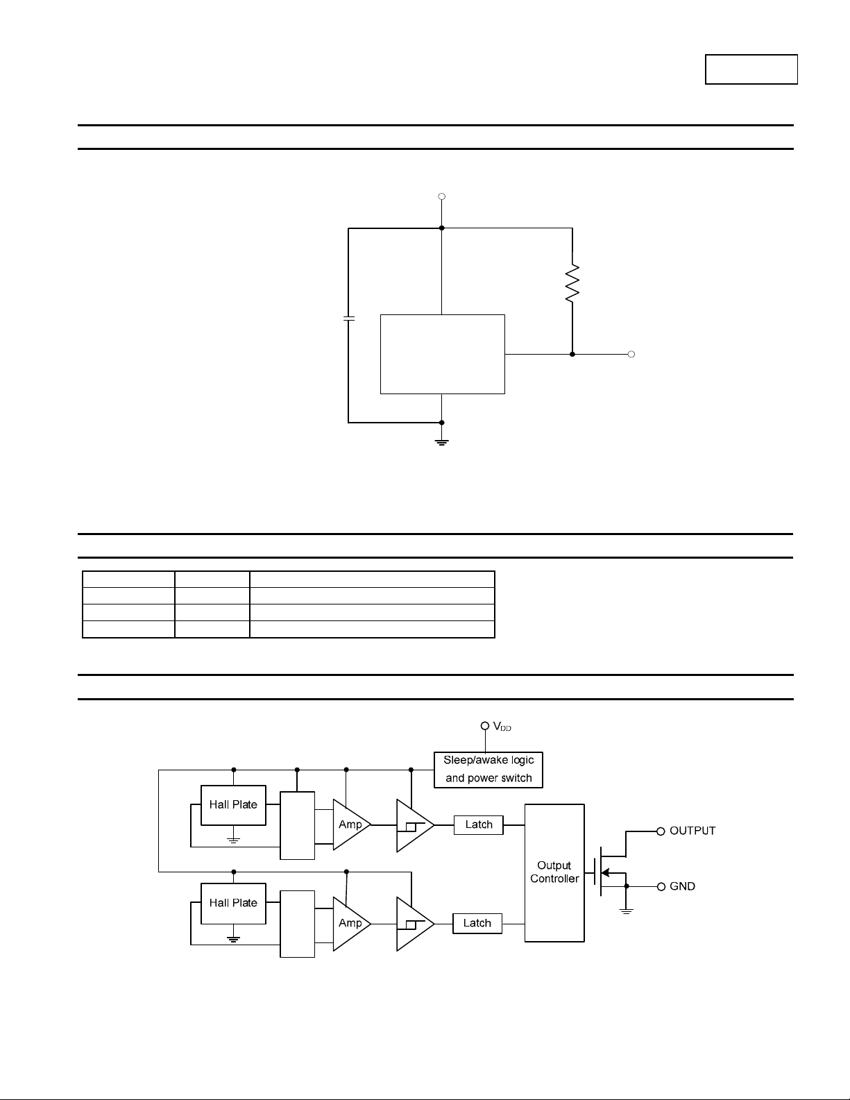
Note: C is for power stabilization and to strengthen the noise immunity, the recommen ded ca pa citance is 10n F ~ 100nF.
is the pull-up resistor, the recommended resistance is 10kOhm ~ 100kOhm.
R
L
Pin Descriptions
Pin Name P/I/O Function
VDD P/I Power Supply Input
GND P/I Ground
Output O Output Pin
Functional Block Diagram
Cancelling
Offset
AH180N
Document number: DS32174 Rev. 4 - 2
Cancelling
Offset
2 of 8
www.diodes.com
August 2012
© Diodes Incorporated

A
H180N
Absolute Maximum Ratings (Note 4) (@T
Symbol Parameter Ratings Unit
VDD Supply Voltage (Note 5) 7 V
B Magnetic Flux Density Unlimited
PD Package Power Dissipation
Ts Storage Temperature Range -65 to +150
TJ Maximum Junction Temperature 150
Notes: 4. Stresses greater than the 'Absolute Maximum Ratings' specified above, may cause permanent damage to the device. These are stress ratings
only; functional operation of the device at these or any other conditions exceeding those indicated in this specification is not implied. Device
reliability may be affected by exposure to absolute maximum rating conditions for extended periods of time
5. The absolute maximum V
operate the device at the absolute maximum rated conditions for any period of time.
of 7V is a transient stress rating and is not meant as a functional operating condition. It is not recommended to
DD
Recommended Operating Conditions (@T
Symbol Parameter Conditions Rating Unit
VDD Supply Voltage Operating 2.5 to 5.5 V
TA Operating Temperature Range Operating -40 to +85
Electrical Characteristics (@T
Symbol Parameter Conditions Min Typ Max Unit
V
Output On Voltage I
OUT
Ioff Output Leakage Current V
Idd(en)
Idd(en)
Idd(dis)
Idd(dis)
Idd(avg)
Idd(avg)
Tawake Awake Time (Note 6)
Tperiod Period (Note 6)
D.C. Duty Cycle
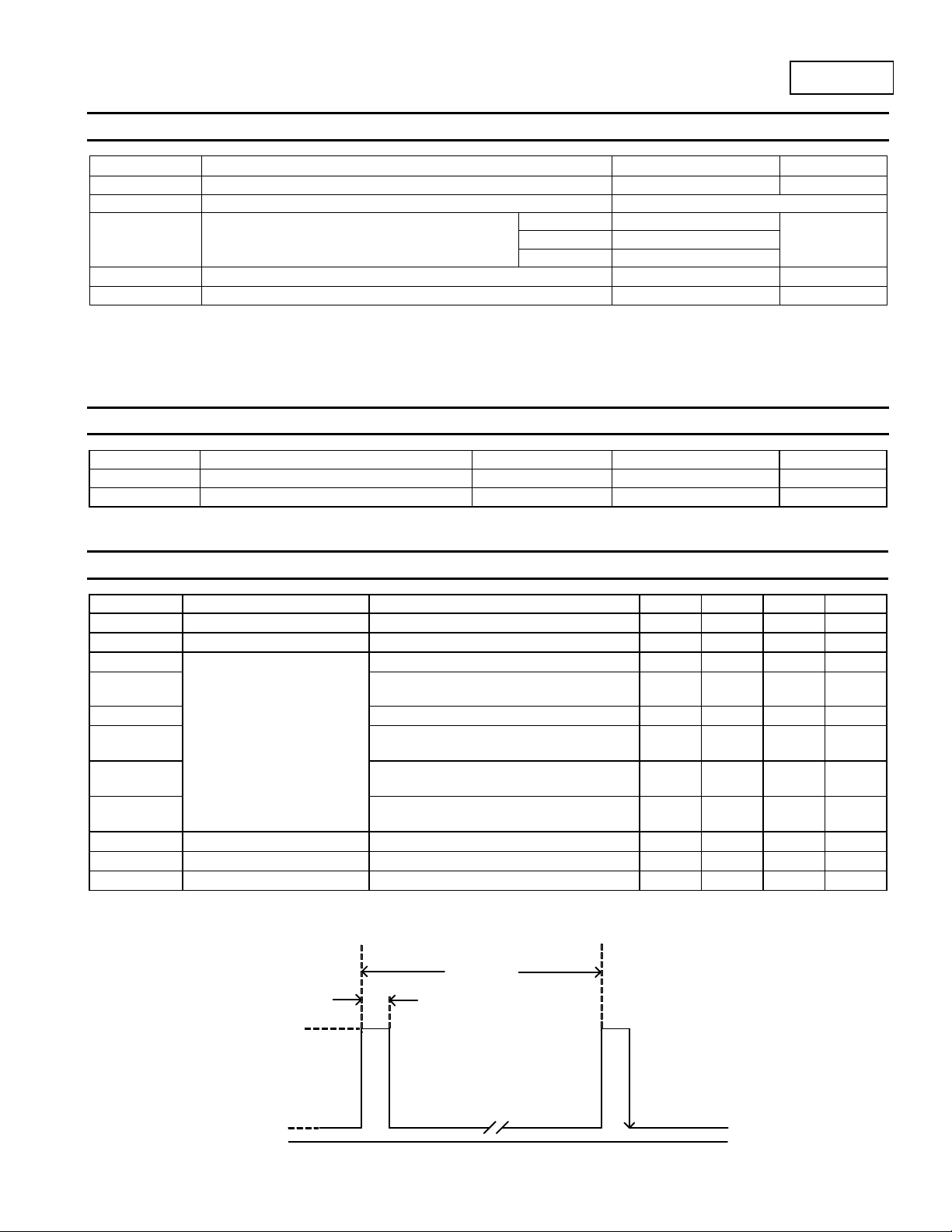
Notes: 6. When power is initially turned on, VDD must be within its correct operating range (2.5V to 5.5V) to guaranteed the output sampling.
The output state is valid after the second operating cycle (typical 150ms).
Supply Current
= +25°C, VDD = 3V, unless otherwise specified.)
A
= +25°C, unless otherwise specified.)
A
SC59 230
SOT553 230
= +25°C, unless otherwise specified.)
A
= 1mA
OUT
= 5.5V, Output Off
OUT
Chip Enable, TA = +25°C, VDD = 3V
Chip Enable, T
V
= 2.5V to 5.5V
DD
Chip Disable, T
Chip Disable, T
V
= 2.5V to 5.5V
DD
= -40 to +85°C,
A
= +25°C, VDD = 3V
A
= -40 to 85°C,
A
Average Supply Current,
T
= +25°C, VDD = 3V
A
Average Supply Current,
T
= -40 to +85°C, VDD = 2.5V to 5.5V
A
⎯
⎯
⎯
⎯
⎯
⎯
⎯
⎯
⎯
⎯
⎯
mW TSOT23 230
°C
°C
°C
0.1 0.3 V
<0.1 1 µA
3 6 mA
3 12 mA
5 10 µA
5 28 µA
8 16 µA
8 40 µA
75 125 µs
75 125 ms
0.1
⎯
%
Idd(en)
Idd (dis)
AH180N
Document number: DS32174 Rev. 4 - 2
Tperiod
Tawake
Sample and output
latched
0
3 of 8
www.diodes.com
August 2012
© Diodes Incorporated
 Loading...