

Page 1
MICROPOWER, ULTRA-SENSITIVE OMNIPOLAR
HALL-EFFECT SENSOR SWITCH
Description
The AH1802 is a ultra-sensitivity, micropower Omnipolar Hall
Effect switch IC designed for portable and battery powered
equipment such as cellular phones, PDA’s and portable
PC’s. Based on two sensitive Hall Effect plates and
a chopper stabilized architecture the AH1802 provides
a reliable solution over the whole operating range. T o support
portable and battery powered equipment the design has been
optimized to operate over the supply range of 2.5V to 5.5V
and consumes only 24uW with a supply of 3V.
The single open drain output can switched on with either a
north or south pole of sufficient strength. When the magnetic
flux density (B) is larger than operate point (Bop) the output is
switched on (pulled low). The output is turned off when
B becomes lower than the release point (Brp). The output will
remain off when there is no magnetic field.
Features
• Omni-polar (north or south pole) operation
• High sensitivity
• Single open drain output
• Micropower operation
• 2.5V to 5.5V operating range
• Chopper stabilized design provides
• Superior temperature stability
• Minimal switch point drift
• Enhanced immunity to stress
• Good RF noise immunity
• -40°C to 85°C operating temperature
• ESD>5kV for DFN2020-6, DFN2020-3 and
DFN2015H4-3
ESD>6kV for SC59
• Low profile SC59, DFN2020-6, DFN2020-3 and
DFN2015H4-3 packages
• “Green” Molding Compound (Note 1)
Notes: 1. EU Directive 2002/95/EC (RoHS). All applicable RoHS exemptions applied. Please visit our website at
http://www.diodes.com/products/lead_free.html.
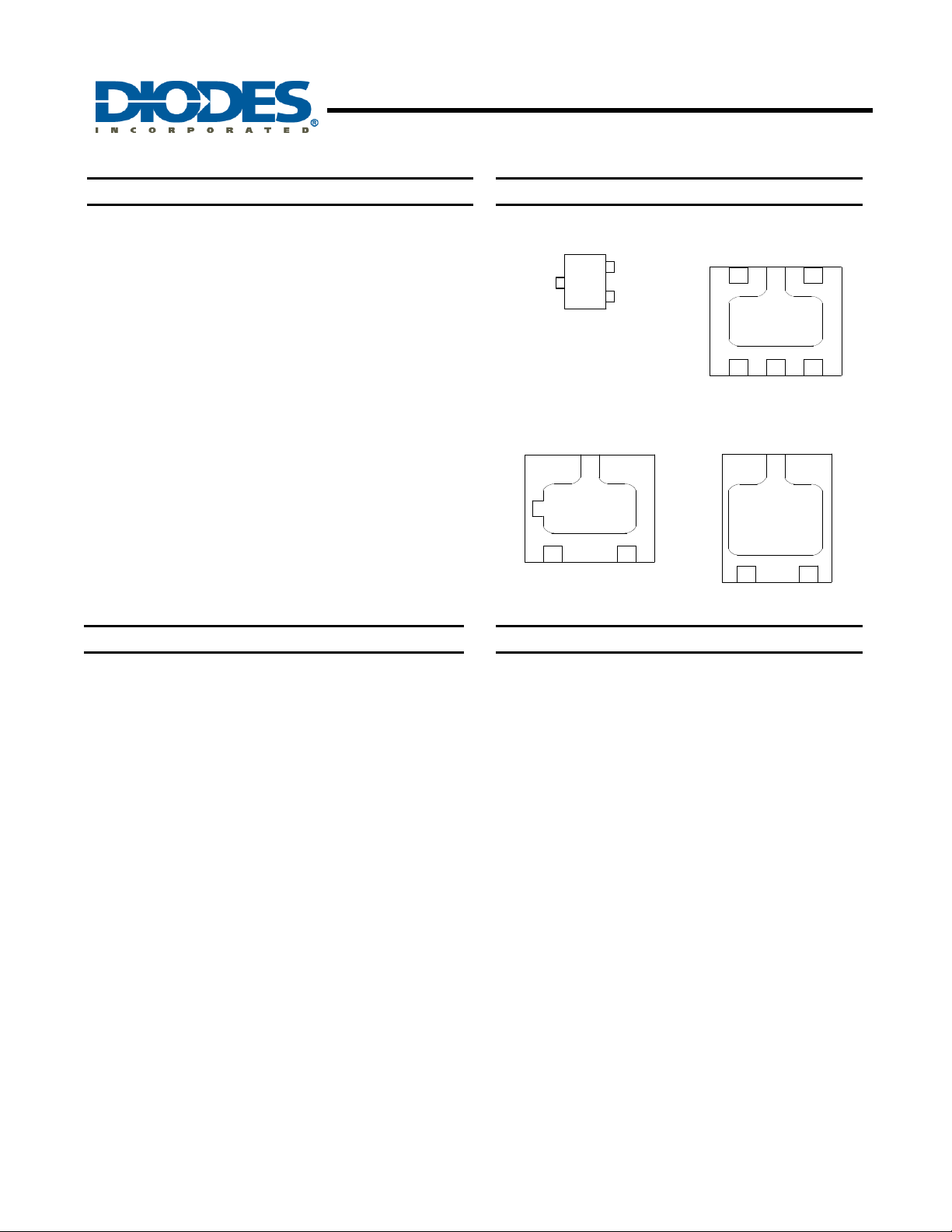
Pin Assignments
(Top View)
2. Output
GND 3.
SC59
(Top View)
1. Vdd
DFN2020-3
1. Vdd
3. GND
3. Output
Applications
• Cover switch in clam-shell or slide type cellular phones
• Display switch for portable PCs
• On/Off switch for PDAs and digital cameras
• Contact-less switch in consumer products
AH1802
(Top View)
5. GND
4. NC6. NC
1. Vdd 2. NC 3. Output
DFN2020-6
(Top View)
3. GND
1. Vdd 2. Output
DFN2015H4-3
AH1802
Document number: 31170 Rev. 8 - 2
1 of 11
www.diodes.com
December 2010
© Diodes Incorporated
Page 2
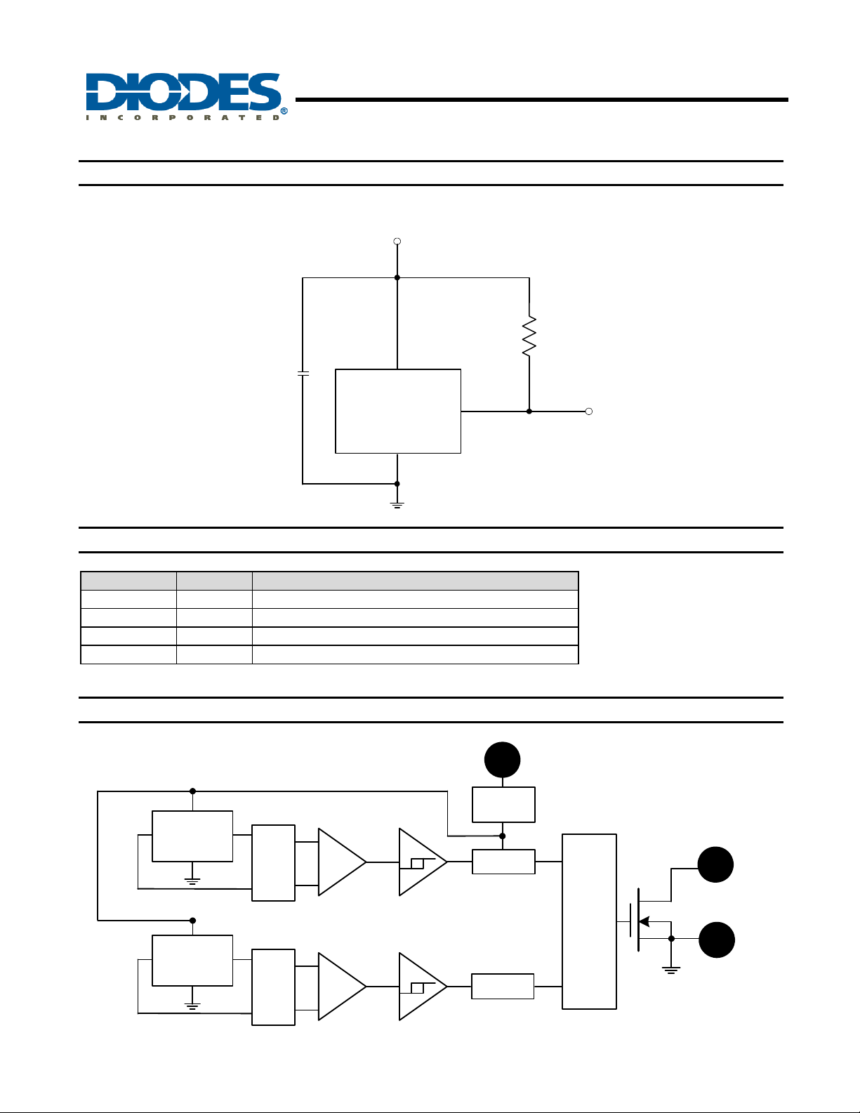
Typical Application Circuit
C
AH1802
MICROPOWER, ULTRA-SENSITIVE OMNIPOLAR
HALL-EFFECT SENSOR SWITCH
2.5~5.5V
R
L
Output
AH1802
GND
Pin Descriptions
Pin Name P/I/O Description
Vdd P/I Power Supply Input
GND P/I Ground
Output O Output Pin
NC No connection (Note 2)
Notes: 2. NC is “No Connection”- recommendation is to connect the NC pin to ground externally.
Functional Block Diagram
1
Power
switch
Latch
Latch
Hall Plate
Hall Plate
Cancelling
Offset
Amp
Cancelling
Offset
Amp
Vdd
Logical
Output
3
GND
2
AH1802
Document number: 31170 Rev. 8 - 2
2 of 11
www.diodes.com
December 2010
© Diodes Incorporated
Page 3
AH1802
V
MICROPOWER, ULTRA-SENSITIVE OMNIPOLAR
HALL-EFFECT SENSOR SWITCH
Absolute Maximum Ratings (T
Symbol Characteristics
Vdd Supply Voltage 7 V
B Magnetic Flux Density Unlimited
Ts Storage Temperature Range -65 to +150
PD Package Power Dissip ation 230 mW
TJ
Maximum Junction Temperature 150
Recommended Operating Conditions (T
Symbol Parameter Conditions Rating Unit
Vdd Supply Voltage Operating 2.5 to 5.5 V
TA Operating Temperature Range Operating -40 to +85
Electrical Characteristics (T
Symbol Characteristic Conditions Min Typ. Max Unit
Vout Output On Voltage Iout=1mA - 0.1 0.3 V
Ioff Output Leakage Current Vout=5.5V, B < Brp -
Idd(en)
Idd(dis)
Idd(avg)
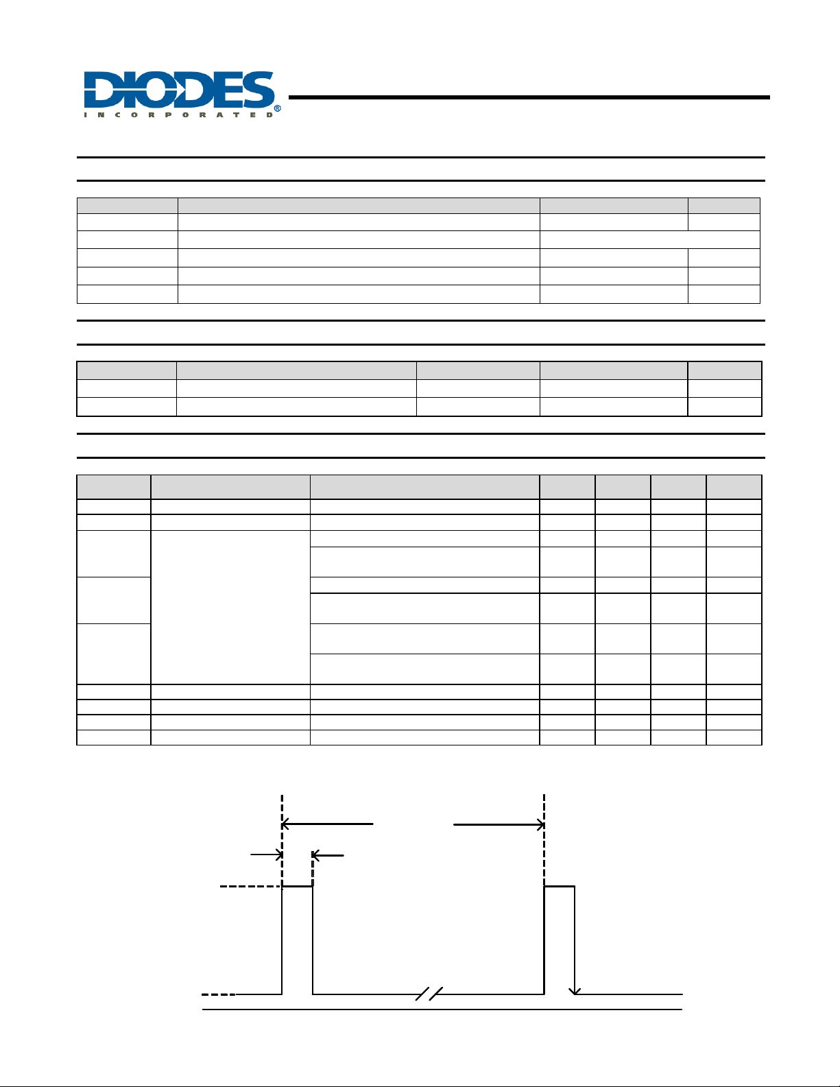
FC Chopping Frequency For design information only - 300 - KHz
Tawake Awake Time (Note 3) - 75 150 µs
Tperiod Period (Note 3) - 75 150 ms
D.C. Duty Cycle - 0.1 - %
Notes: 3. When power is initially turned on, Vdd must be within its correct operating range (2.5V to 5.5V) to guaranteed the output sampling.
The output state is valid after the second operating cycle (typical 150ms).
Supply Current
= 25°C)
A
= 25°C)
A
= 25°C, Vdd = 3V; unless otherwise specified)
A
Chip enable, T
Chip enable, TA= -40~85°C,
Vdd = 2.5~5.5V
Chip disable, T
Chip disable, TA= -40~85°C,
Vdd = 2.5~5.5V
Average supply current ,
TA= 25°C, Vdd = 3V
Average supply current ,
= -40~85°C, Vdd = 2.5~5.5V
T
A
= 25°C, Vdd = 3V
A
= 25°C, Vdd = 3V
A
- 3 6 mA
- 3 10 mA
- 5 10 µA
- 5 18 µA
- 8 16 µA
- 8 23 µA
alues Unit
°C
°C
°C
<0.1
1 µA
Tperiod
Tawake
Idd(en)
Sample and output
latched
Idd (dis)
0
AH1802
Document number: 31170 Rev. 8 - 2
3 of 11
www.diodes.com
December 2010
© Diodes Incorporated
Page 4
MICROPOWER, ULTRA-SENSITIVE OMNIPOLAR
HALL-EFFECT SENSOR SWITCH
Magnetic Characteristics (T
Symbol Characteristic Min Typ. Max Unit
Bops(south pole to brand side)
Bopn(north pole to brand side) -40 -28 -20
Brps(south pole to brand side)
Brpn(north pole to brand side) - -20 -10
Bhy( BrpxBopx − )
Notes: 4. Typical data is at TA = 25°C, Vdd = 3V, and for design information only.
5. The magnetic characteristics may vary with supply voltage, operating temperature and after soldering.
= 25°C, Vdd = 3V, Note 4 & 5)
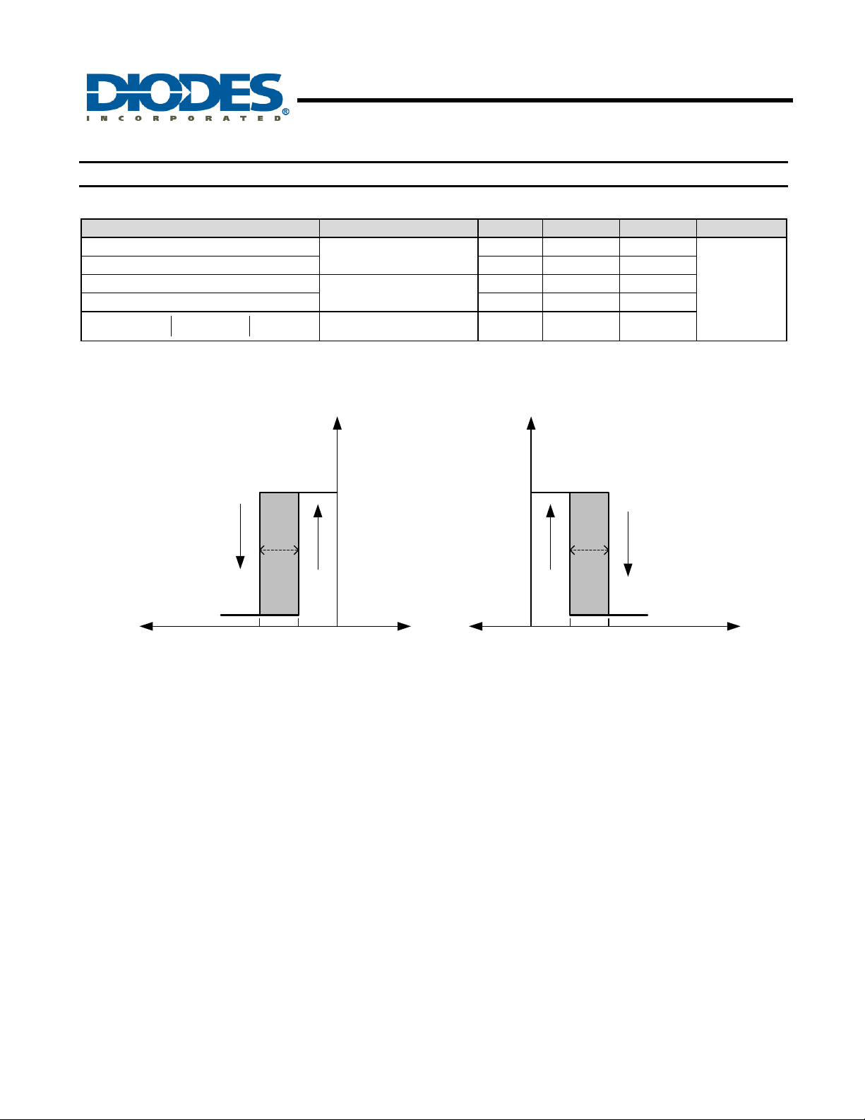
A
Operate Point
Release Point
Hysteresis 5 8 -
Output
20 28 40
10 20 -
Output
AH1802
(1mT=10 Gauss)
Gauss
Vcc
Turn on
( Output Voltage )
( on-state )
( Magnetic flux density B )
AH1802
Document number: 31170 Rev. 8 - 2
( off-state )
Bhy
Bopn Brpn 0
Turn off
Vsat
( Output Voltage )
4 of 11
www.diodes.com
Turn off
( off-state )
Bhy
Vcc
Turn on
( on-state )
Vsat
Brps Bops0
( Magnetic flux density B )
December 2010
© Diodes Incorporated
Page 5

AH1802
MICROPOWER, ULTRA-SENSITIVE OMNIPOLAR
HALL-EFFECT SENSOR SWITCH
Performance Characteristics
TA (°C)
PD (mW) 230 184 166 147 129 120 110 92 74 55 37 18 0
25 50 60 70 80 85 90 100 110 120 130 140 150
P
(mW )
D
300
200
100
0
0 25 50 75 100 125 150
Power Dissipation C urve
85-40
TA (oC)
Ordering Information
AH 1802 - XXX G – 7 - 01
Package
W : SC59
SN : DFN2020-6
FJ : DFN2020-3
FY4 : DFN2015H4-3
Green
G : Green
Packing
7 : Tape & Reel
Taping orientation
01: 180
o
rotation
Note 8
Device
AH1802-WG-7 W SC59 3000/Tape & Reel -7
AH1802-SNG-7 SN DFN2020-6 3000/Tape & Reel -7
AH1802-FJG-7 FJ DFN2020-3 3000/Tape & Reel -7
AH1802-FJG-7-01 (Note 8) FJ DFN2020-3 3000/Tape & Reel -7
AH1802-FY4G-7 FY4 DFN2015H4-3 3000/Tape & Reel -7
Notes: 6. EU Directive 2002/95/EC (RoHS). All applicable RoHS exemptions applied. Please visit our website at
http://www.diodes.com/products/lead_free.html.
7. Pad layout as shown on Diodes Inc. suggested pad layout document AP02001, which can be found on our website at
http://www.diodes.com/datasheets/ap02001.pdf.
8. AH1802-FJG-7-01 DFN2020-3 package taping orientation is rotated by 180
See package orientation diagrams on page 10.
Package
Code
Packaging
(Note 6 & 7)
Quantity Part Number Suffix
o
compared to standard part AH1802-FJG-7.
7” Tape and Reel
AH1802
Document number: 31170 Rev. 8 - 2
5 of 11
www.diodes.com
December 2010
© Diodes Incorporated
Page 6

Marking Information
(1) SC59
AH1802
MICROPOWER, ULTRA-SENSITIVE OMNIPOLAR
HALL-EFFECT SENSOR SWITCH
( Top View )
(2) DFN2020-6
(3) DFN2020-3
XX
3
Y W
X
XX : Identification code
: Year 0~9
Y
: Week : A~Z : 1~26 week;
W
a~z : 27~52 week; z represents
52 and 53 week
: A~Z : Green
1 2
Part Number Package Identification Code
AH1802 SC59 KC
X
( Top View )
Pin 1 indicator
XX
XX
Y
WX
: Iden tific ation Co d e
Y : Y e a r : 0~9
: Week : A~Z : 1~26 week;
W
a~z : 27~52 week; z represents
52 and 53 week
X
: A~Z : G re e n
Part Number Package Identification Code
AH1802 DFN2020-6 KC
AH1802
Document number: 31170 Rev. 8 - 2
( Top View )
Pin 1 indicator
: Ide ntification Code
XX
Y
WX
XX
Y : Year : 0~9
W
: We e k : A~Z : 1~26 week;
a~z : 27~52 week; z represents
52 and 53 week
X
: A~Z : Green
Part Number Package Identification Code
AH1802 DFN2020-3 KE
6 of 11
www.diodes.com
December 2010
© Diodes Incorporated
Page 7

MICROPOWER, ULTRA-SENSITIVE OMNIPOLAR
Marking Information (Continued)
(4) DFN2015H4-3
( Top View )
Pin 1 indicator
XX
XX
WX
Y
Part Number Package Identification Code
AH1802 DFN2015H4-3 KF
Package Outline Dimensions (All Dimensions in mm)
(1) Package Type: SC59
: Identification Code
Y : Ye a r : 0 ~ 9
: Week : A~Z : 1~26 week;
W
a~z : 27~52 week; z represents
52 and 53 week
X
: A~Z : Green
AH1802
HALL-EFFECT SENSOR SWITCH
AH1802
Document number: 31170 Rev. 8 - 2
7 of 11
www.diodes.com
December 2010
© Diodes Incorporated
Page 8

Package Outline Dimensions (Continued)
(2) Package Type: DFN2020-6
AH1802
MICROPOWER, ULTRA-SENSITIVE OMNIPOLAR
HALL-EFFECT SENSOR SWITCH
0.57/0.63
0.05 C
0.08 C
B
1.95/2.075
0.15 C
2x-
(3) Package type: DFN2020-3
0/0.05
2x
Pin#1 ID
C
L
0.76/0.96
0.65nom.
Marking
C
0.15
1.95/2.075
1.45/1.65
C
L
Bottom View
0.43mon.
(Active area depth)
0.15max.
C
A
Sensor location
0.30/0.40
R
0
.
1
0.2/0.3
0.05
Seating plane
0.37
M C A B
Top View
0.65
0.150.15
0.45
C
L
0.37
C
L
0.9
1.67
Land Pattern Recommendation
(Unit:mm)
0.47/0.53
0.10 C
0.08 C
B
1.85/2.15
0.25 B
2x-
AH1802
Document number: 31170 Rev. 8 - 2
0/0.05
0.10
R
0.775/0.975
0
.
2
C
L
M C A B
2x
Top Marking
C
L
0.5Typ
Pin1
0.2/0.3
1.1/1.35 0.325
1.85/2.15
Bottom View
0.25 A
Seating plane
C
Sensor location
0.35/0.45
0.138
A
www.diodes.com
0.18±0.07
8 of 11
1.25 0.325
0.3
C
L
0.138
C
L
0.925
2.4
0.65
Pin1
1
0.3
0.5
Land Pattern Recommendation
(Unit:mm)
Top View
December 2010
© Diodes Incorporated
Page 9

Package Outline Dimensions (Continued)
(4) Package type: DFN2015H4-3
Top Mark
0.10 C
3x-
0.08 C
2x-
0.25
0.40Max.
0.125Typ.
B
1.95/2.075
B
0/0.05
A
0.25
2x-
0.25/0.35
(Pin #1)
0.20/0.30
Bottom View
Side View
1.45/1.575
2x-0.50
Hall Sensor
1.0/1.2
C
L
AH1802
MICROPOWER, ULTRA-SENSITIVE OMNIPOLAR
HALL-EFFECT SENSOR SWITCH
C
L
5
7
1
.
(Pin #1)
1.30Typ.
C
L
0.50
0.50
(Unit:mm)
Top View
3x-0.35
0.15
1.0Typ.
0.45
0.10
C
L
0.13Typ.
C
A
0.7/0.9
C
Seating Plane
0
R
Land Pattern Recommendation
AB
AH1802
Document number: 31170 Rev. 8 - 2
9 of 11
www.diodes.com
December 2010
© Diodes Incorporated
Page 10

MICROPOWER, ULTRA-SENSITIVE OMNIPOLAR
Taping Orientation
(1) DFN2020-6 and DFN2020-3 with standard taping orientation
AH1802
HALL-EFFECT SENSOR SWITCH
(2) DFN2020-3 with 180o rotation from standard taping orientation
(3) DFN2015H4-3
Notes: 9. The taping orientation of the other package type can be found on our website at http://www.diodes.com/datasheets/ap02007.pdf.
AH1802
Document number: 31170 Rev. 8 - 2
10 of 11
www.diodes.com
December 2010
© Diodes Incorporated
Page 11

AH1802
MICROPOWER, ULTRA-SENSITIVE OMNIPOLAR
HALL-EFFECT SENSOR SWITCH
IMPORTANT NOTICE
DIODES INCORPORATED MAKES NO WARRANTY OF ANY KIND, EXPRESS OR IMPLIED, WITH REGARDS TO THIS
DOCUMENT, INCLUDING, BUT NOT LIMITED TO, THE IMPLIED WARRANTIES OF MERCHANTABILITY AND FITNESS FOR A
PARTICULAR PURPOSE (AND THEIR EQUIVALENTS UNDER THE LAWS OF ANY JURISDICTION).
Diodes Incorporated and its subsidiaries reserve the right to make modifications, enhancements, improvements, corrections or other
changes without further notice to this document and any product described herein. Diodes Incorporated does not assume any liability
arising out of the application or use of this document or any product described herein; neither does Diodes In corporated convey any
license under its patent or trademark rights, nor the rights of others. Any Customer or user of this documen t or products described
herein in such applications shall assume all risks of such use and will agree to hold Diodes Incorporated and all the companies
whose products are represented on Diodes Incorporated website, harmless against all damages.
Diodes Incorporated does not warrant or accept any liability whatsoever in respect of any products purchased through unauthorized
sales channel.
Should Customers purchase or use Diodes Incorporated products for any unintended or unauthorized application, Customers shall
indemnify and hold Diodes Incorporated and its representatives harmless against all claims, damages, expenses, and attorney fees
arising out of, directly or indirectly, any claim of personal injury or death associated with such unintended or unauthorized application.
Products described herein may be covered by one or more United States, international or foreign p atents pending. Product names
and markings noted herein may also be covered by one or more United States, international or foreign trademarks.
LIFE SUPPORT
Diodes Incorporated products are specifically not authorized for use as critical components in life support devices or systems without
the express written approval of the Chief Executive Officer of Diodes Incorporated. As used herein:
A. Life support devices or systems are devices or systems which:
1. are intended to implant into the body, or
2. support or sustain life and whose failure to perform when properly used in accordance with instructions for use provided
in the labeling can be reasonably expected to result in significant injury to the user.
B. A critical component is any component in a life support device or system whose failure to perform can be reasonably expected
to cause the failure of the life support device or to affect its safety or effectiveness.
Customers represent that they have all necessary expertise in the safety and regulatory ramifications of their life support dev ices or
systems, and acknowledge and agree that they are solely responsible for all legal, regulatory and safety-related requirements
concerning their products and any use of Diodes Incorporated products in such safety-critical, life support devices or systems,
notwithstanding any devices- or systems-related information or support that may be provided by Diodes Incorporated. Further,
Customers must fully indemnify Diodes Incorporated and its representatives against any damages arising out of the use of Diodes
Incorporated products in such safety-critical, life support devices or systems.
Copyright © 2010, Diodes Incorporated
www.diodes.com
AH1802
Document number: 31170 Rev. 8 - 2
11 of 11
www.diodes.com
December 2010
© Diodes Incorporated
 Loading...