

Page 1
AH173
INTERNAL PULL-UP HALL EFFECT LATCH FOR HIGH
TEMPERATURE
Description
AH173 is a single-digital-output Hall-Effect latch sensor with
pull-up resistor for high temperature operation. The device
includes an on-chip Hall voltage generator for magnetic
sensing, an amplifier to amplify Hall voltage, a comparator to
provide switching hysteresis for noise rejection, and an
output driver with a pull-up resistor (Rpu). An internal bandgap regulator provides a temperature compensated supply
voltage for internal circuits and allows a wide operating
supply range.
When the magnetic flux density (B) is larger than operate
point (Bop), output is switched on (OUT pin is pulled low).
The output state is held on until a magnetic flux density
reversal falls below Brp. When B is less than Brp, the output
is switched off.
The AH173 is available in SIP-3L and SC59 packages.
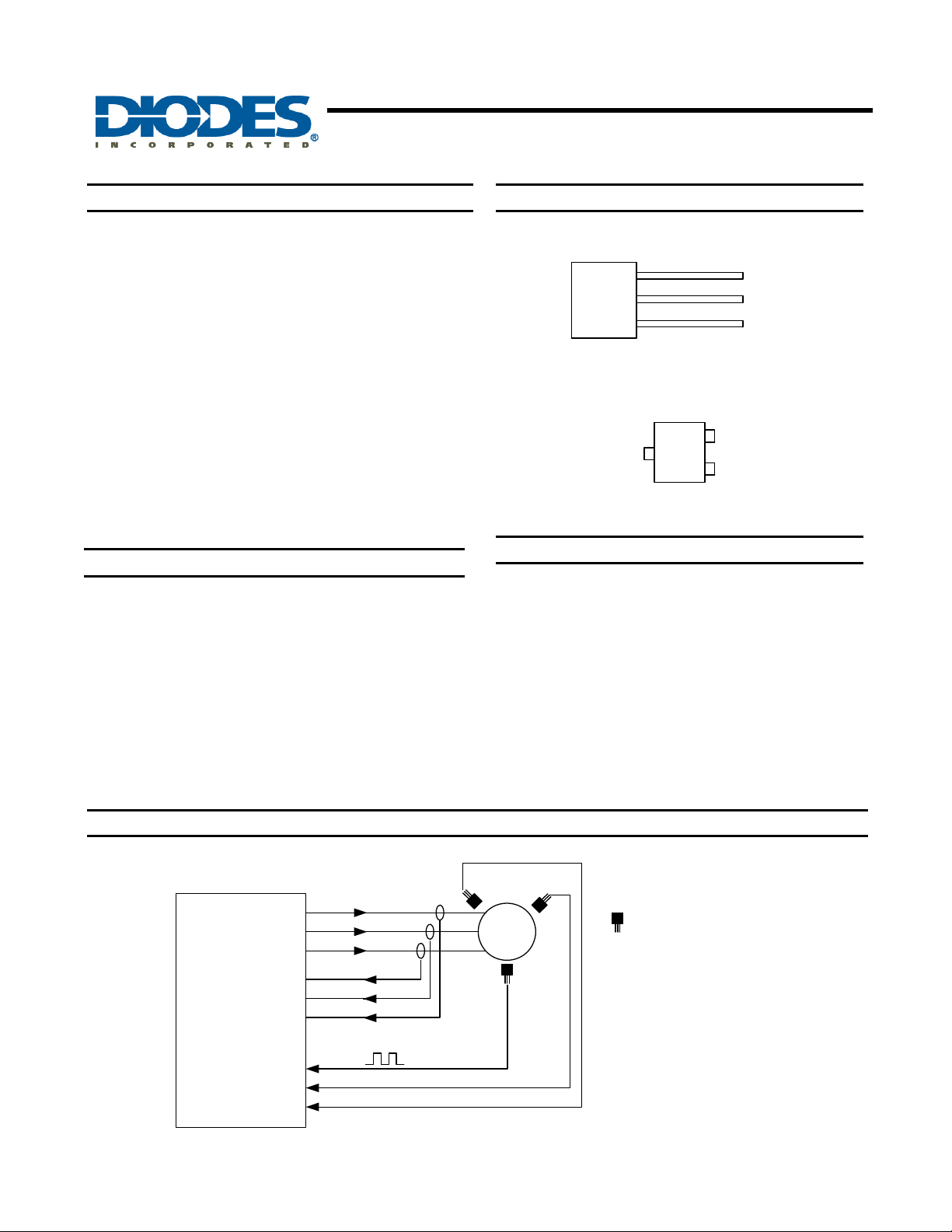
Pin Assignments
(Top View)
SIP-3L
(Top View)
GND 2.
SC59
Applications
Features
• Bipolar Hall-Effect latch sensor
• 3V to 20V DC operating voltage
• Built-in pull-up resistor
• 25mA output sink current
• Operating temperature: -40°C to +125°C
• SIP-3L and SC59 packages
(SC59 is commonly known as SOT23 in Asia)
• Green Molding Compound (No Br, Sb) (Note 1)
Notes: 1. EU Directive 2002/95/EC (RoHS). All applicable RoHS exemptions applied. Please visit our website at
http://www.diodes.com/products/lead_free.html.
• Rotor Position Sensing
• Current Switch
• Encoder
• RPM Detection
3.
2.
1.
3. OUT
1. Vcc
OUT
GND
Vcc
Typical Application Circuit
IA
IB
Driver
&
IC
Ia
Ib
Ic
Control Logic
HA
HB
HC
Hall Motor Driver
AH173
Document number: DS31044 Rev. 10 - 2
M
RPM sensing
3 Phase Hall Motor
1 of 9
www.diodes.com
Digital Hall Effect Sensor
M: Three Phase Hall Motor
July 2010
© Diodes Incorporated
Page 2
INTERNAL PULL-UP HALL EFFECT LATCH FOR HIGH
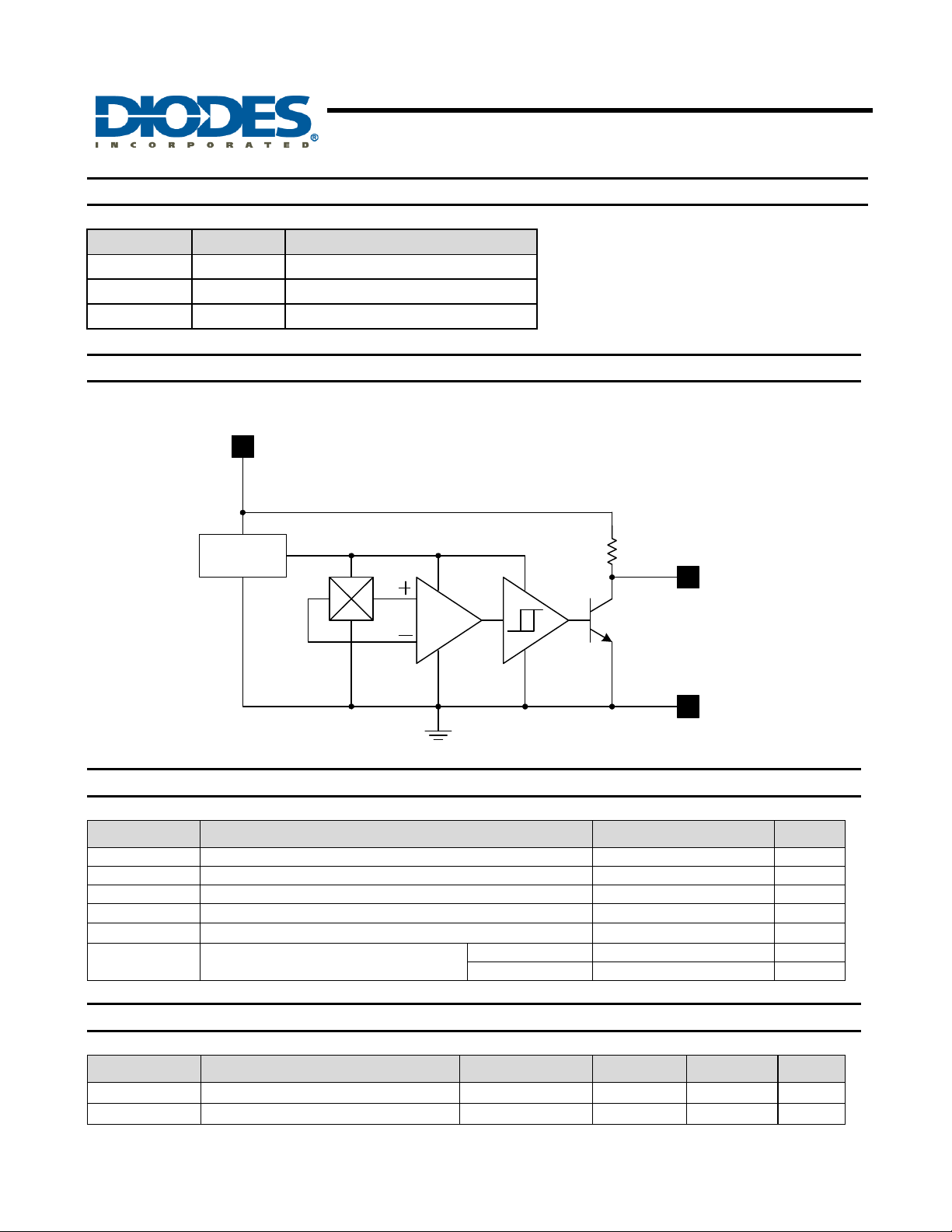
Pin Descriptions
Pin Name Pin # Description
Vcc 1 Positive Power Supply
GND 2 Ground
OUT 3 Output Stage
Functional Block Diagram
V
CC
1
AH173
TEMPERATURE
REG.
AMP
Absolute Maximum Ratings (T
Symbol Characteristics Values Unit
VCC Supply Voltage 20 V
V
(off) Output “Off” Voltage 20 V
OUT
IO (sink) Output “On” Current 25 mA
Ts Storage Temperature Range -65~+150
TJ Maximum Junction Temperature +150
PD Power Dissipation
= 25°C)
A
SIP-3L 550 mW
SC59 230 mW
Rpu
3
2
OUT
GND
°C
°C
Recommended Operating Conditions
Symbol Characteristic Conditions Min Max Unit
VCC Supply Voltage Operating 3 20 V
TA Operating Ambient Temperature Operating -40 125
AH173
Document number: DS31044 Rev. 10 - 2
2 of 9
www.diodes.com
© Diodes Incorporated
°C
July 2010
Page 3
AH173
INTERNAL PULL-UP HALL EFFECT LATCH FOR HIGH
TEMPERATURE
Electrical Characteristics (T
Symbol Characteristics Conditions Min Typ. Max Unit
V
OUT (SAT)
Output Saturation Voltage
ICC Supply Current VCC = 12V, OUT ”OFF” - 3.5 6 mA
Rpu Internal Pull-up Resistor 7 10 13
Vd Dropout Voltage
Magnetic Characteristics (T
A grade
Symbol Parameter Min Typ. Max Unit
Bops(south pole to brand side) Operation Point 15 - 60 Gauss
Brps(south pole to brand side) Release Point -60 - -15 Gauss
Bhy(|Bopx|-|Brpx|) Hysteresis - 80 - Gauss
B grade
Symbol Parameter Min Typ. Max Unit
Bops(south pole to brand side) Operation Point 5 - 80 Gauss
Brps(south pole to brand side) Release Point -80 - -5 Gauss
Bhy(|Bopx|-|Brpx|) Hysteresis - 80 - Gauss
Notes: 2. Magnetic characteristics may vary with supply voltage, operating temperature and after soldering.
= 25°C)
A
V
= 12V, OUT ”ON”
CC
I
= 10mA
O
= V
CC
- VCe
V
d
= 25°C, Vcc = 12V, unless otherwise specified, Note 2)
A
- 300 400 mV
- - 0.3 V
(1mT = 10 Gauss)
KΩ
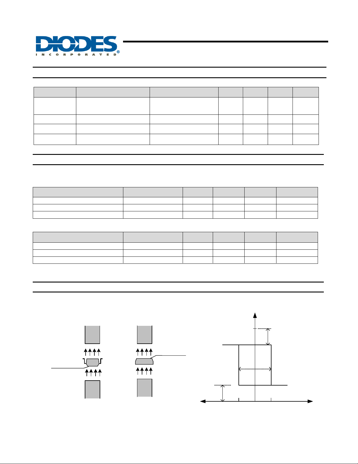
Operating Characteristics
S
Marking Side
N
(SC59)
AH173
Document number: DS31044 Rev. 10 - 2
S
N
(SIP-3L)
Marking Side
3 of 9
www.diodes.com
V
out
V
cc
High
Voltage)
B
(Output
V
SAT
rp
B
0
(Magnetic Flux Density)
V
d
hy
Low
op
B
July 2010
© Diodes Incorporated
Page 4

Performance Characteristics
(1) SIP-3L
TA (°C)
PD (mW)
TA (°C)
PD(mW)
(mW )
P
D
25 50 60 70 80 85 90 95 100
550 440 396 352 308 286 264 242 220
105 110 115 120 125 130 135 140 150
198 176 154 132 110 88 66 44 0
600
500
400
300
200
AH173
INTERNAL PULL-UP HALL EFFECT LATCH FOR HIGH
TEMPERATURE
P o wer Dis sip a tio n C u rve
100
0
0 25 50 75 100 125 150
-40
(2) SC59 (commonly known as SOT23 in Asia)
TA (°C)
PD (mW)
25 50 60 70 80 85 90 100 110 120 130 140 150
230 184 166 147 129 120 110 92 74 55 37 18 0
(mW )
P
D
300
200
100
Po we r D is sipa tion C u rve
T
A
(°C )
0
AH173
Document number: DS31044 Rev. 10 - 2
0 25 50 75 100 125 150
-40
(°C )
T
A
4 of 9
www.diodes.com
July 2010
© Diodes Incorporated
Page 5

Ordering Information
AH173
INTERNAL PULL-UP HALL EFFECT LATCH FOR HIGH
TEMPERATURE
Package
P : SIP-3L
W : SC59
L : Lead Free
G : Green (Note 3)
AH173 - X X - X - X
Lead Free
Packing
A : Ammo Box (Note 6)
B : Bulk (Note 7)
Magnetic
Characteristics
A or B
7 : Tape & Reel
Tube/Bulk 7” Tape and Reel Ammo Box
Magnetic
Characteristics
Code
Packaging
(Note 4, 5)
Quantity
Part
Number
Suffix
Quantity
Part
Number
Suffix
Quantity
Part
Number
Suffix
Package
Device
AH173-PL-A-A P SIP-3L NA NA NA NA 4000/Box -A A
AH173-PL-A-B P SIP-3L NA NA NA NA 4000/Box -A B
AH173-PG-A-A P SIP-3L NA NA NA NA 4000/Box -A A
AH173-PG-A-B P SIP-3L NA NA NA NA 4000/Box -A B
AH173-PL-B-A P SIP-3L 1000 -B NA NA NA NA A
AH173-PL-B-B P SIP-3L 1000 -B NA NA NA NA B
AH173-PG-B-A P SIP-3L 1000 -B NA NA NA NA A
AH173-PG-B-B P SIP-3L 1000 -B NA NA NA NA B
AH173-WL-7-A W SC59 NA NA 3000/Tape & Reel -7 NA NA A
AH173-WL-7-B W SC59 NA NA 3000/Tape & Reel -7 NA NA B
AH173-WG-7-A W SC59 NA NA 3000/Tape & Reel -7 NA NA A
AH173-WG-7-B W SC59 NA NA 3000/Tape & Reel -7 NA NA B
Notes: 3. EU Directive 2002/95/EC (RoHS). All applicable RoHS exemptions applied. Please visit our website at
http://www.diodes.com/products/lead_free.html.
4. Pad layout as shown on Diodes Inc. suggested pad layout document AP02001, which can be found on our website at
http://www.diodes.com/datasheets/ap02001.pdf.
5. Reverse taping as shown on Diodes Inc. Surface Mount (SMD) Packaging document AP02007, which can be found on our
website http://www.diodes.com/datasheets/ap02007.pdf.
6. Ammo Box is for SIP-3L Spread Lead.
7. Bulk is for SIP-3L Straight Lead.
AH173
Document number: DS31044 Rev. 10 - 2
5 of 9
www.diodes.com
July 2010
© Diodes Incorporated
Page 6

INTERNAL PULL-UP HALL EFFECT LATCH FOR HIGH
Marking Information
(1) SIP-3L
(Top View)
Part Number
(2) SC59 (Commonly known as SOT23 in Asia)
173
WW X
Y
: Year : 0~9
Y
WW
: Week : 01~52, "52" represents
52 and 53 week
X
: Internal Code : A~Z : Green
AH173
TEMPERATURE
a~z : Lead Free
(Top View)
XX : Identification code
: Year 0~9
Y
: Week : A~Z : 1~26 week;
XX Y W
X
W
a~z : 27~52 week; z represents
52 and 53 week
: A~Z : Green
X
a~z : Lead Free
Part Number Package Identification Code
AH173 SC59 J3
AH173
Document number: DS31044 Rev. 10 - 2
6 of 9
www.diodes.com
July 2010
© Diodes Incorporated
Page 7

INTERNAL PULL-UP HALL EFFECT LATCH FOR HIGH
Package Outline Dimensions (All Dimensions in mm)
(1) Package Type: SIP-3L for Bulk pack
0.51mm
NOM
2.00 +/-
0.10mm
AH173
TEMPERATURE
1.15 +/-
0.10mm
Package Dimension
BRANDED
SURFACE
123
Active Area Depth Sensor Location
AH173
Document number: DS31044 Rev. 10 - 2
7 of 9
www.diodes.com
July 2010
© Diodes Incorporated
Page 8

INTERNAL PULL-UP HALL EFFECT LATCH FOR HIGH
Package Outline Dimensions (Continued)
(2) Package Type: SIP-3L for Ammo pack
AH173
TEMPERATURE
(3) SC59 (Commonly known as SOT23 in Asia)
0.35/0.50
1.00/
1.30
0.013/0.10
TOP VIEW
1.90
2.90/3.10
0.95
2.70/
1.50/
1.70
3.00
0.35/0.55
0.10/0.20
AH173
Document number: DS31044 Rev. 10 - 2
O
0O/8
8 of 9
www.diodes.com
July 2010
© Diodes Incorporated
Page 9

AH173
INTERNAL PULL-UP HALL EFFECT LATCH FOR HIGH
TEMPERATURE
IMPORTANT NOTICE
DIODES INCORPORATED MAKES NO WARRANTY OF ANY KIND, EXPRESS OR IMPLIED, WITH REGARDS TO THIS
DOCUMENT, INCLUDING, BUT NOT LIMITED TO, THE IMPLIED WARRANTIES OF MERCHANTABILITY AND FITNESS FOR A
PARTICULAR PURPOSE (AND THEIR EQUIVALENTS UNDER THE LAWS OF ANY JURISDICTION).
Diodes Incorporated and its subsidiaries reserve the right to make modifications, enhancements, improvements, corrections or other
changes without further notice to this document and any product described herein. Diodes Incorporated does not assume any liability
arising out of the application or use of this document or any product described herein; neither does Diodes In corporated convey any
license under its patent or trademark rights, nor the rights of others. Any Customer or user of this documen t or products described
herein in such applications shall assume all risks of such use and will agree to hold Diodes Incorporated and all the companies
whose products are represented on Diodes Incorporated website, harmless against all damages.
Diodes Incorporated does not warrant or accept any liability whatsoever in respect of any products purchased through unauthorized
sales channel.
Should Customers purchase or use Diodes Incorporated products for any unintended or unauthorized application, Customers shall
indemnify and hold Diodes Incorporated and its representatives harmless against all claims, damages, expenses, and attorney fees
arising out of, directly or indirectly, any claim of personal injury or death associated with such unintended or unauthorized application.
Products described herein may be covered by one or more United States, international or foreign p atents pending. Product names
and markings noted herein may also be covered by one or more United States, international or foreign trademarks.
LIFE SUPPORT
Diodes Incorporated products are specifically not authorized for use as critical components in life support devices or systems without
the express written approval of the Chief Executive Officer of Diodes Incorporated. As used herein:
A. Life support devices or systems are devices or systems which:
1. are intended to implant into the body, or
2. support or sustain life and whose failure to perform when properly used in accordance with instructions for use provided
in the labeling can be reasonably expected to result in significant injury to the user.
B. A critical component is any component in a life support device or system whose failure to perform can be reasonably expected
to cause the failure of the life support device or to affect its safety or effectiveness.
Customers represent that they have all necessary expertise in the safety and regulatory ramifications of their life support dev ices or
systems, and acknowledge and agree that they are solely responsible for all legal, regulatory and safety-related requirements
concerning their products and any use of Diodes Incorporated products in such safety-critical, life support devices or systems,
notwithstanding any devices- or systems-related information or support that may be provided by Diodes Incorporated. Further,
Customers must fully indemnify Diodes Incorporated and its representatives against any damages arising out of the use of Diodes
Incorporated products in such safety-critical, life support devices or systems.
Copyright © 2010, Diodes Incorporated
www.diodes.com
AH173
Document number: DS31044 Rev. 10 - 2
9 of 9
www.diodes.com
July 2010
© Diodes Incorporated
 Loading...