Diodes 74LVCE1G126 User Manual
74LVCE1G126
SINGLE BUFFER GATE WITH 3-STATE OUTPUT
Description
The 74LVCE1G126 is a single non-inverting buffer/bus driver
with a 3-state output. The output enters a high impedance
state when a LOW-level is applied to the output enable (OE)
pin. The device is designed for operation with a power supply
range of 1.4V to 5.5V. The inputs are tolerant to 5.5V
allowing this device to be used in a mixed voltage
environment. The device is fully specified for partial power
down applications using I
output preventing damaging current backflow when the device
is powered down.
. The I
OFF
circuitry disables the
OFF
Features
NEW PRODUCT
• Extended Supply Voltage Range from 1.4 to 5.5V
• Switching speed characterized for operation at 1.5V
• Offers 30% speed improvement over LVC at 1.8V.
• ± 24mA Output Drive at 3.3V
• CMOS low power consumption
• IOFF Supports Partial-Power-Down Mode Operation
• Inputs accept up to 5.5V
• ESD Protection Tested per JESD 22
Exceeds 200-V Machine Model (A115-A)
Exceeds 2000-V Human Body Model (A114-A)
• Latch-Up Exceeds 100mA per JESD 78, Class II
• Range of Package Options
• Direct Interface with TTL Levels
• SOT25, SOT353 and DFN1410: Assembled with “Green”
Molding Compound (no Br, Sb)
• Lead Free Finish/ RoHS Compliant (Note 1)
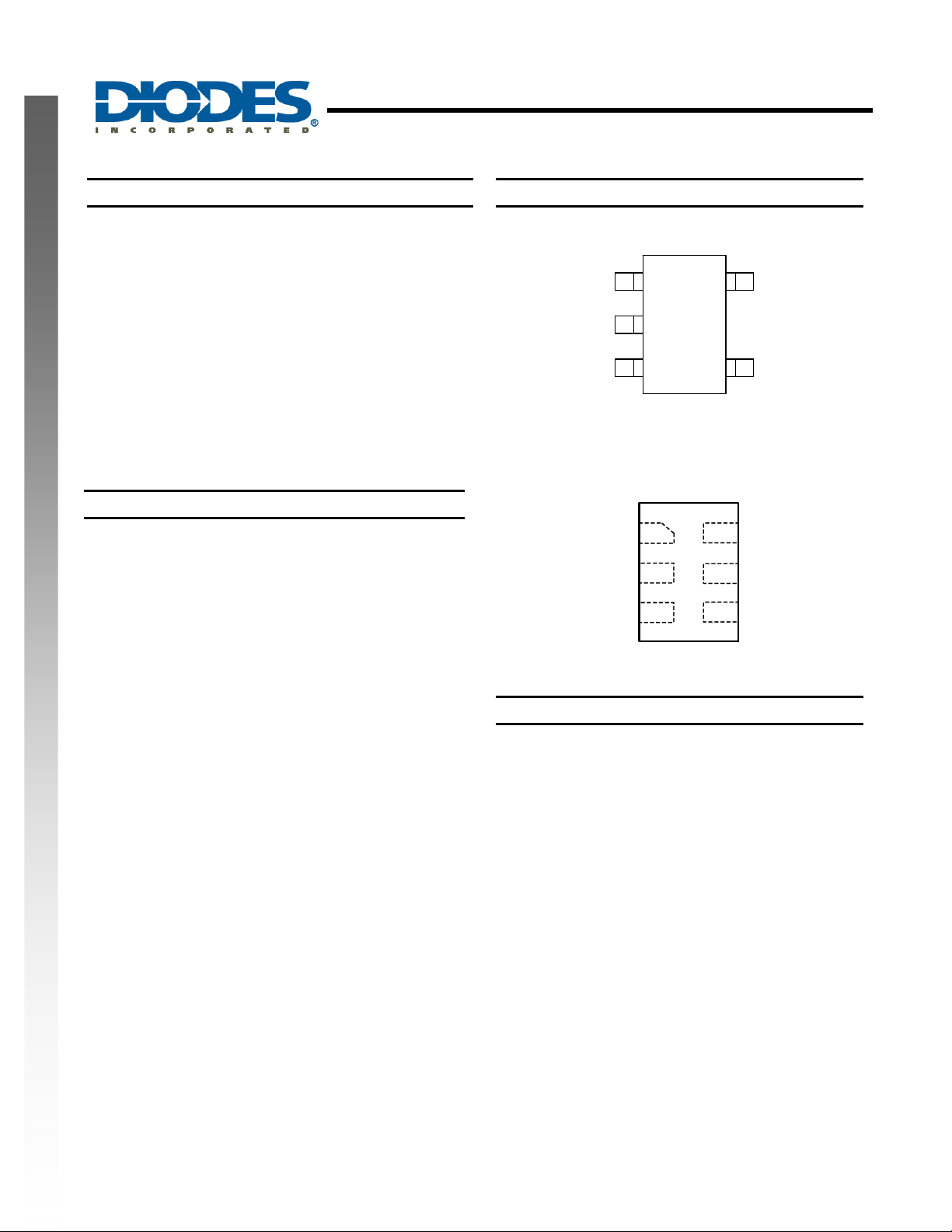
Pin Assignments
(Top View)
OE
A
GND
1
2
Vcc
5
43
Y
SOT25 / SOT353
(Top View)
1
OE
2
A
GND
3
DFN1410 (Note 2)
6
Vcc
5
NC
4
Y
Applications
• Voltage Level Shifting
• Bus Driver / Repeater
• Power Down Signal Isolation
• General Purpose Logic
• Wide array of products such as.
o PCs, networking, notebooks, netbooks, PDAs
o Computer peripherals, hard drives, CD/DVD ROM
o TV, DVD, DVR, set top box
o Cell Phones, Personal Navigation / GPS
o MP3 players ,Cameras, Video Recorders
Notes: 1. EU Directive 2002/95/EC (RoHS). All applicable RoHS exemptions applied. Please visit our website at
74LVCE1G126
Document number: DS32217 Rev. 3 - 2
http://www.diodes.com/products/lead_free.html.
2. Pin 2 and pin 5 of the DFN1410 package are internally connected.
1 of 14
www.diodes.com
February 2011
© Diodes Incorporated
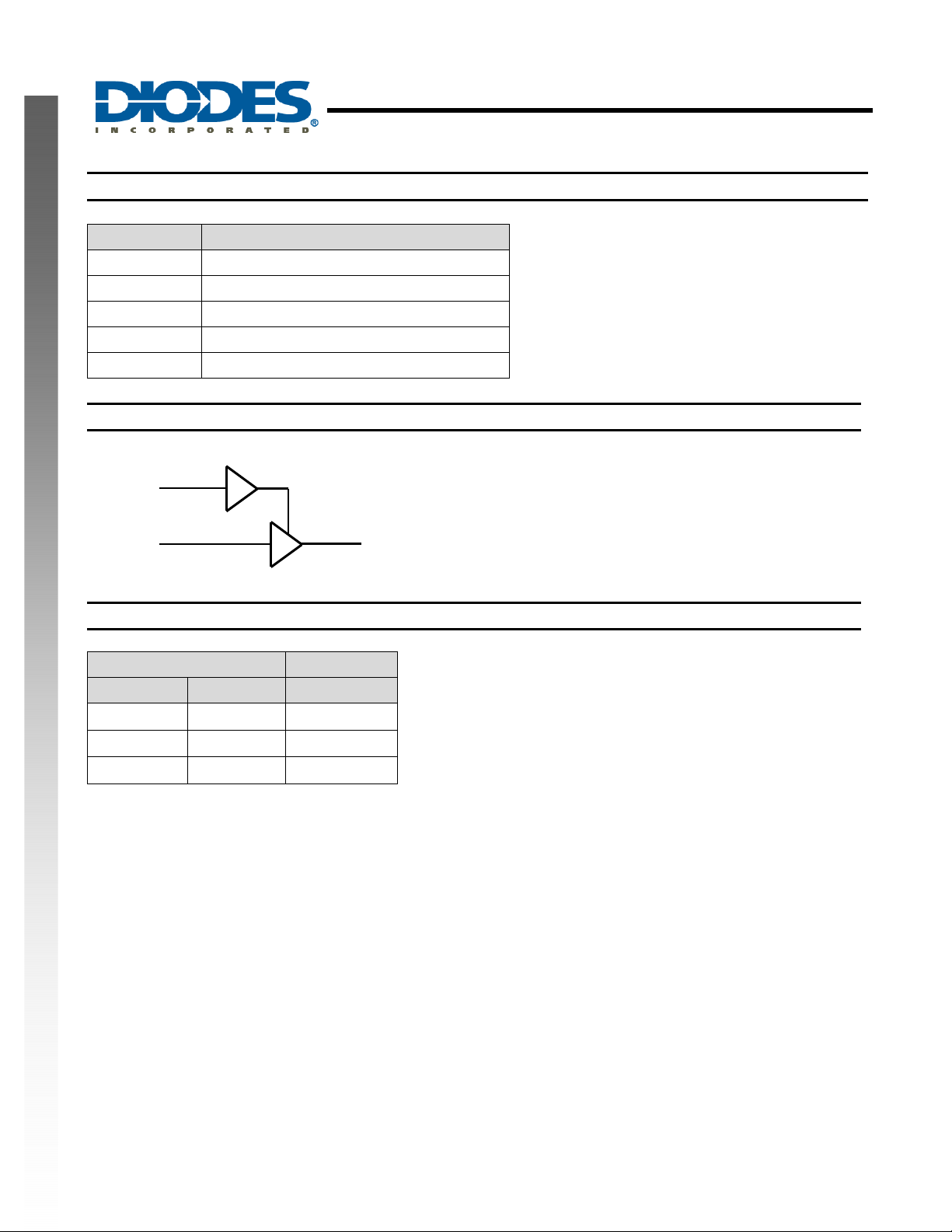
Pin Descriptions
Pin Name Description
OE
A
GND
Y
Vcc
Logic Diagram
OE
NEW PRODUCT
A
SINGLE BUFFER GATE WITH 3-STATE OUTPUT
Output Enable (active high)
Data Input
Ground
Data Output
Supply Voltage
1
2 4
Y
74LVCE1G126
Function Table
Inputs Output
OE
H
H
L
A
H
L
X
Y
H
L
Z
74LVCE1G126
Document number: DS32217 Rev. 3 - 2
2 of 14
www.diodes.com
February 2011
© Diodes Incorporated
74LVCE1G126
SINGLE BUFFER GATE WITH 3-STATE OUTPUT
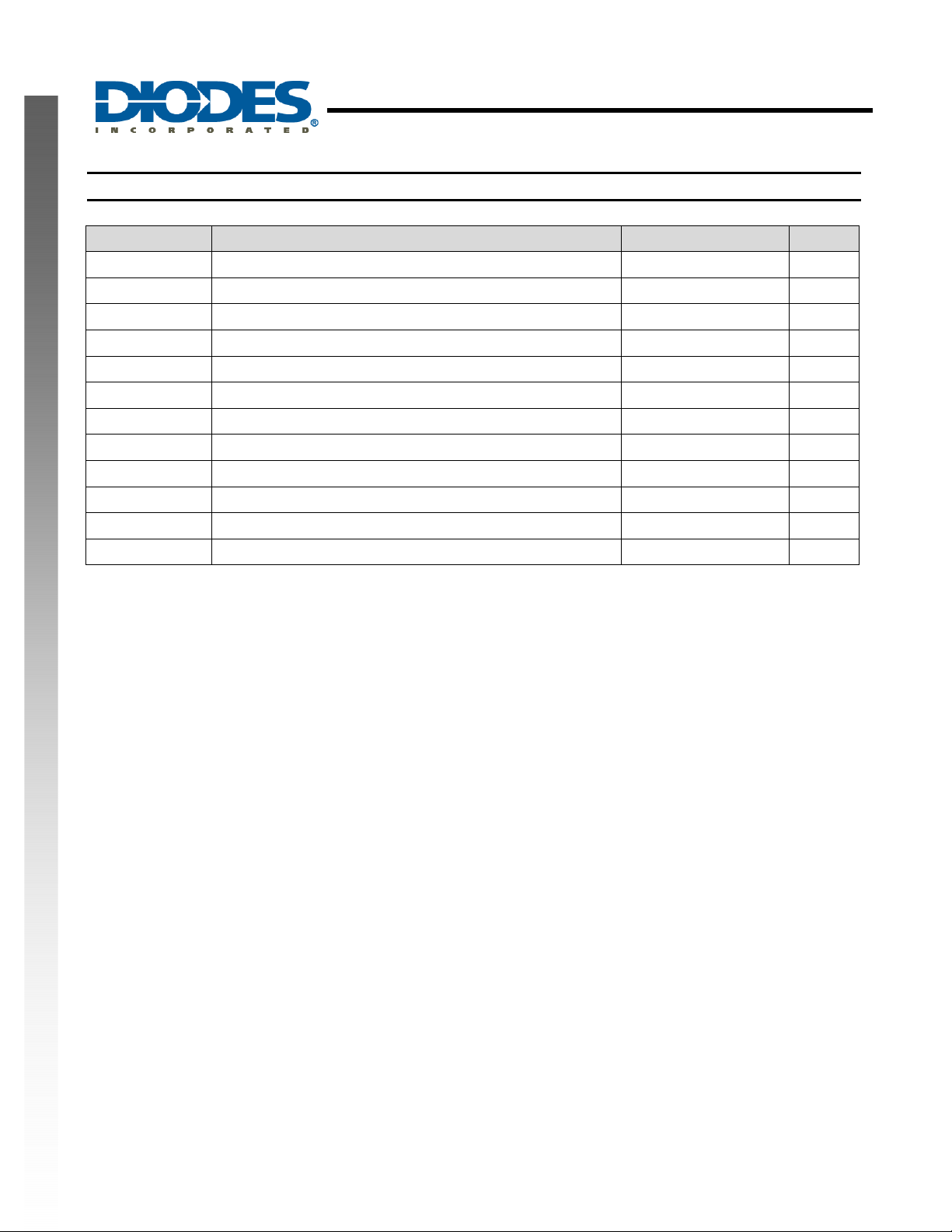
Absolute Maximum Ratings (Note 3)
Symbol Description Rating Unit
ESD HBM Human Body Model ESD Protection 2 KV
ESD MM Machine Model ESD Protection 200 V
VCC Supply Voltage Range -0.5 to 6.5 V
VI Input Voltage Range -0.5 to 6.5 V
Vo Voltage applied to output in high impedance or I
Vo Voltage applied to output in high or low state -0.3 to VCC +0.5 V
IIK Input Clamp Current VI<0 -50 mA
IOK Output Clamp Current -50 mA
IO Continuous output current ±50 mA
Continuous current through Vdd or GND ±100 mA
TJ Operating Junction Temperature -40 to 150 °C
NEW PRODUCT
T
Storage Temperature -65 to 150 °C
STG
Note: 3. Stresses beyond the absolute maximum may result in immediate failure or reduced reliability. These are stress values and device
operation should be within recommend values.
state -0.5 to 6.5 V
OFF
74LVCE1G126
Document number: DS32217 Rev. 3 - 2
3 of 14
www.diodes.com
February 2011
© Diodes Incorporated
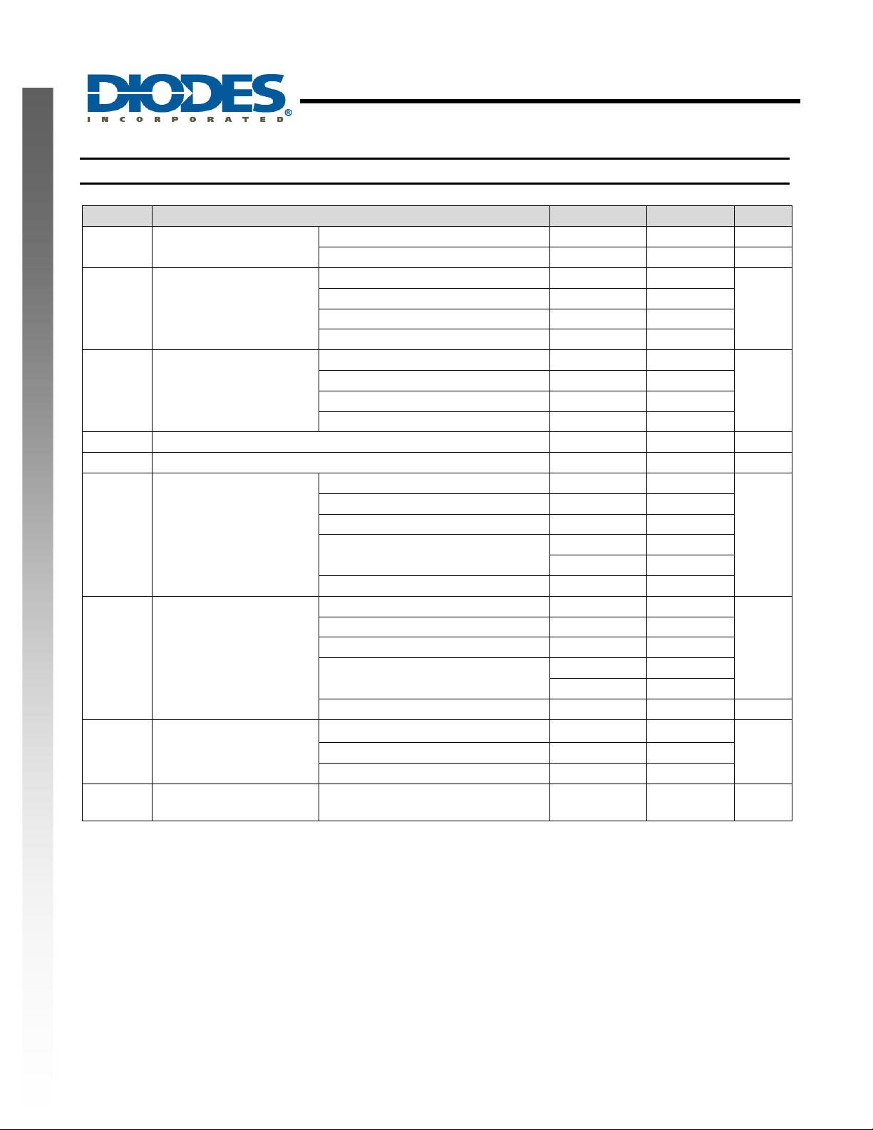
Recommended Operating Conditions (Note 4)
Symbol Parameter Min Max Unit
VCC Operating Voltage
V
High Level Input Voltage
IH
VIL Low Level Input Voltage
VI Input Voltage 0 5.5 V
VO Output Voltage 0 VCC V
NEW PRODUCT
IOH
IOL
Δt/ΔV
TA
Note: 4. Unused inputs should be held at Vcc or Ground.
High Level Output
Current
Low Level Output
Current
Input transition rise or fall
rate
Operating free-air
temperature
Operating 1.4 5.5 V
Data retention only 1.2 V
V
= 1.4 V to 1.95 V 0.65 X VCC
CC
VCC = 2.3 V to 2.7 V 1.7
VCC = 3 V to 3.6 V 2
VCC = 4.5 V to 5.5 V 0.7 X VCC
V
= 1.4 V to 1.95 V 0.35 X VCC
CC
VCC = 2.3 V to 2.7 V 0.7
VCC = 3 V to 3.6 V 0.8
VCC = 4.5 V to 5.5 V 0.3 X VCC
Vcc=1.4 V -3
VCC = 1.65 V -4
VCC = 2.3 V -8
VCC = 3 V
VCC = 4.5 V -32
Vcc=1.4 V 3
VCC = 1.65 V 4
VCC = 2.3 V 8
VCC = 3 V
VCC = 4.5 V 32
V
= 1.4 to 3V
CC
VCC = 3.3 V ± 0.3 V 10
VCC = 5 V ± 0.5 V 5
74LVCE1G126
SINGLE BUFFER GATE WITH 3-STATE OUTPUT
V
V
-16
-24
16
24
20
-40 85 ºC
mA
mA
ns/V
74LVCE1G126
Document number: DS32217 Rev. 3 - 2
4 of 14
www.diodes.com
February 2011
© Diodes Incorporated
74LVCE1G126
SINGLE BUFFER GATE WITH 3-STATE OUTPUT
Electrical Characteristics (All typical values are at Vcc = 3.3V, T
Over recommended free-air temperature range (unless otherwi se noted)
Symbol Parameter Test Conditions Vcc Min Typ. Max Unit
= -100μA 1.4 V to 5.5V V
I
OH
IOH = -3mA 1.4 V 1.05
VOH
VOL
High Level Output
Voltage
Low Level Output
Voltage
NEW PRODUCT
II Input Current VI = 5.5 V or GND 0 to 5.5 V ± 5 μA
I
OFF
IOZ
ICC Supply Current
ΔICC
Ci Input Capacitance Vi = V
θ
θ
Note: 5. Test condition for SOT25, SOT353 and DFN1410: Device mounted on FR-4 substrate PC board, 2oz copper, with minimum
recommended pad layout.
Power Down Leakage
Current
Z State
Leakage Current
Additional Supply
Current
Thermal Resistance
JA
Junction-to-Ambient
Thermal Resistance
JC
Junction-to-Case
IOH = -4mA 1.65 V 1.2
IOH = -8mA 2.3V 1.9
IOH = -16mA
IOH = -24mA 2.3
3 V
IOH = -32mA 4.5 V 3.8
= 100μA 1.4 V to 5.5V 0.1
I
OL
IOL = 3mA 1.4V .4
IOL = 4mA 1.65 V 0.45
IOL = 8mA 2.3V 0.3
IOL = 16mA
IOL = 24mA 0.55
3 V
IOL = 32mA 4.5 0.55
V
or VO = 5.5V 0
I
V
=0 to 5.5V 3.6V
O
V
= 5.5V of GND
I
=0
I
O
One input at V
CC
–
1.4 V to 5.5V
3 V to 5.5V
0.6 V Other inputs
at V
or GND
CC
– or GND 3.3 3.5 pF
CC
SOT25 (Note 5) 204
DFN1410 (Note 5) 430
SOT25 (Note 5) 52
SOT353
(Note 5)
DFN1410 (Note 5) 190
= 25°C)
A
– 0.1
CC
2.4
0.4
143
± 10 μA
10 μA
10 μA
500 μA
V
V
o
C/WSOT353 (Note 5) 371
o
C/W
74LVCE1G126
Document number: DS32217 Rev. 3 - 2
5 of 14
www.diodes.com
February 2011
© Diodes Incorporated
 Loading...