Diodes 74AUP1G34 User Manual

uture
oduct
74AUP1G34
SINGLE BUFFER GATE
Description
The Advanced Ultra Low Power (AUP) CMOS logic family is designed
for low power and extended battery life in portable applications.
The 74AUP1G34 is a single buffer gate with a standard push-pull
output designed for operation over a power supply range of 0.8V to
3.6V. The device is fully specified for partial power down applications
OFF
. The I
using I
current backflow when the device is powered down.
The gate performs the positive Boolean function:
AY
circuitry disables the output preventing damaging
OFF
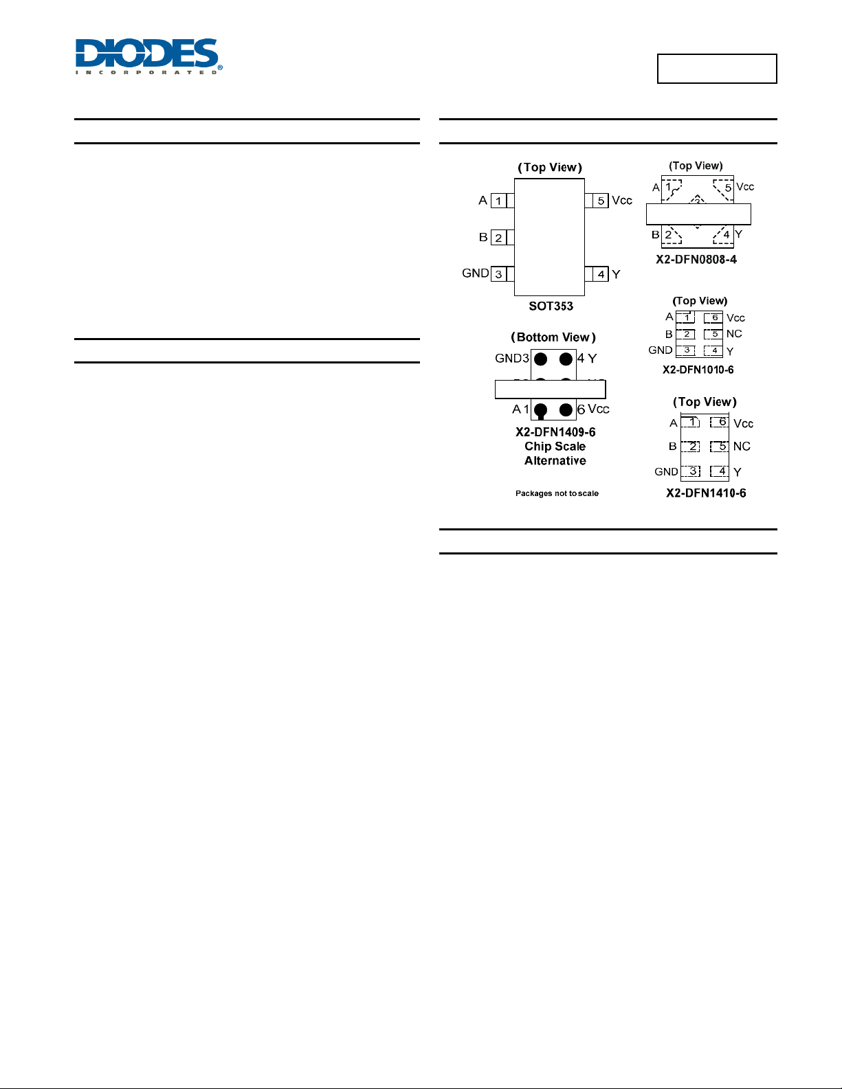
Pin Assignments
Future Product
Features
Advanced Ultra Low Power (AUP) CMOS
Supply Voltage Range from 0.8V to 3.6V
±4mA Output Drive at 3.0V
Low Static power consumption
< 0.9µA
I
CC
Low Dynamic Power Consumption
C
= 6.3pF (Typical at 3.6V)
PD
Schmitt Trigger Action at All Inputs Make the Circuit Tolerant for
Slower Input Rise and Fall Time. The hysteresis is typically
250mV at V
I
Exceeds 1000-V Charged Device Model (C101C)
Latch-Up Exceeds 100mA per JESD 78, Class II
Leadless packages named per JESD30E
Totally Lead-Free & Fully RoHS Compliant (Notes 1 & 2)
Halogen and Antimony Free. “Green” Device (Note 3)
Notes: 1. No purposely added lead. Fully EU Directive 2002/95/EC (RoHS) & 2011/65/EU (RoHS 2) compliant.
2. See http://www.diodes.com for more information about Diodes Incorporated’s definitions of Halogen- and Antimony-free, "Green" and Lead-free.
3. Halogen- and Antimony-free "Green” products are defined as those which contain <900ppm bromine, <900ppm chlorine (<1500ppm total Br + Cl) and
<1000ppm antimony compounds.
Supports Partial-Power-Down Mode Operation
OFF
ESD Protection Exceeds JESD 22
2000-V Human Body Model (A114-A)
74AUP1G34
Document number: DS35155 Rev. 2 - 2
= 3.0V
CC
Applications
Suited for battery and low power needs
Wide array of products such as:
Click here for ordering information, located at the end of datasheet
1 of 14
www.diodes.com
F
Pr
Tablets, E-readers
Cell Phones, Personal Navigation / GPS
MP3 players ,Cameras, Video Recorders
PCs ultrabooks, notebooks, netbooks,
Computer peripherals, hard drives, CD/DVD ROM
TV, DVD, DVR, set top box
© Diodes Incorporated
July 2013

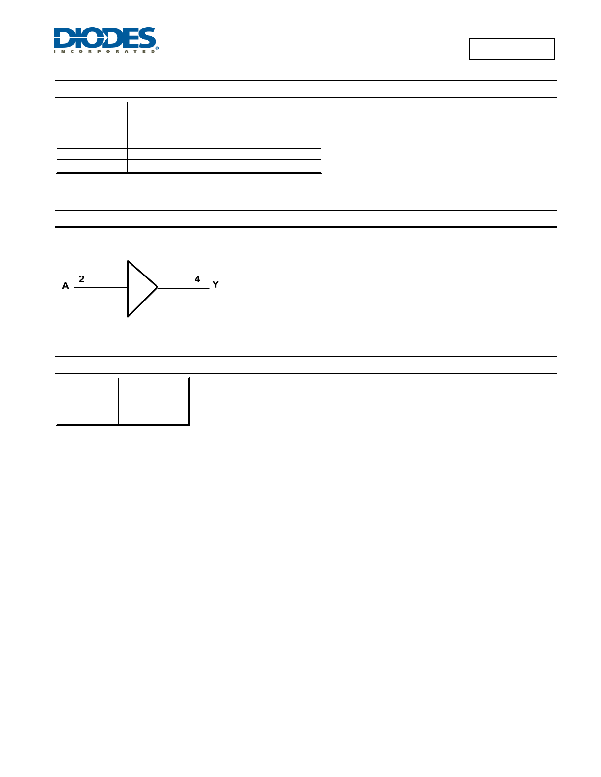
Pin Descriptions
Pin Name Function
NC No Connection
A Data Input
GND Ground
Y Data Output
VCC
Supply Voltage
Logic Diagram
74AUP1G34
Function Table
Inputs Output
A Y
H H
L L
74AUP1G34
Document number: DS35155 Rev. 2 - 2
2 of 14
www.diodes.com
July 2013
© Diodes Incorporated

74AUP1G34
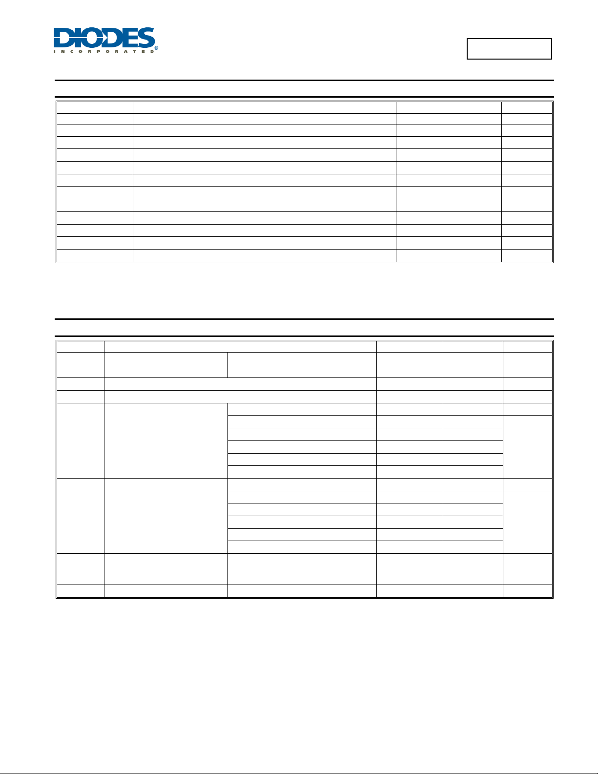
Absolute Maximum Ratings (Note 4) (@T
Symbol Parameter Rating Unit
ESD HBM Human Body Model ESD Protection 2 kV
ESD CDM Charged Device Model ESD Protection 1 kV
VCC
VI
Vo
IIK Input Clamp Current VI < 0
IOK Output Clamp Current (VO < 0 )
IO Continuous Output Current (VO = 0 to VCC)
ICC Continuous Current Through VCC
I
GND
TJ
T
STG
Note: 4. Stresses beyond the absolute maximum may result in immediate failure or reduced reliability. These are stress values and device operation should be
within recommend values.
Supply Voltage Range -0.5 to +4.6 V
Input Voltage Range -0.5 to +4.6 V
Voltage Applied to Output in High or Low State
Continuous Current Through GND -50 mA
Operating Junction Temperature -40 to +150 °C
Storage Temperature -65 to +150 °C
Recommended Operating Conditions (Note 5) (@T
Symbol Parameter Min Max Unit
VCC
Operating Voltage
= +25°C, unless otherwise specified.)
A
-0.5 to VCC +0.5
50 mA
50 mA
±20 mA
50 mA
= +25°C, unless otherwise specified.)
A
0.8 3.6 V
V
VI
VO
IOH
IOL
Δt/ΔV Input Transition Rise or Fall Rate
TA
Note: 5. Unused inputs should be held at VCC or Ground.
Input Voltage 0 3.6 V
Output Voltage 0
V
CC
VCC = 1.1V
High-Level output current
Low-Level output current
Operating Free-Air Temperature
VCC = 1.4V
VCC = 1.65V
VCC = 2.3V
VCC = 3.0V
V
CC
VCC = 1.1V
VCC = 1.4V
VCC = 1.65V
VCC = 2.3V
VCC = 3.0V
V
CC
74AUP1G34
Document number: DS35155 Rev. 2 - 2
= 0.8V
= 0.8V
= 0.8V to 3.6V
www.diodes.com
3 of 14
VCC
-20 µA
-1.1
-1.7
-1.9
-3.1
-4
20 µA
1.1
1.7
1.9
3.1
4
200 ns/V
-40 +125 °C
V
mA
mA
July 2013
© Diodes Incorporated

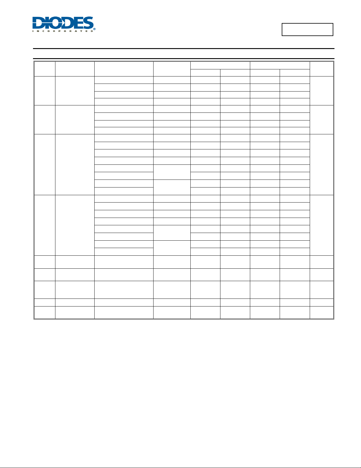
Electrical Characteristics (@T
= +25°C, unless otherwise specified.)
A
74AUP1G34
Symbol Parameter Test Conditions
0.8V to 1.65V
High-Level Input
V
IH
Voltage
1.65V to 1.95V
2.3V to 2.7V 1.6 1.6
3.0V to 3.6V 2.0 2.0
0.8V to 1.65V
VIL
Low-Level Input
Voltage
1.65V to 1.95V
2.3V to 2.7V 0.7 0.7
3.0V to 3.6V 0.9 0.9
I
= -20μA
OH
IOH = -1.1mA
IOH = -1.7mA
VOH
High-Level
Output Voltage
IOH = -1.9mA
IOH = -2.3mA
IOH = -3.1mA
IOH = -2.7mA
IOH = -4mA
I
= 20μA
OL
IOL = 1.1mA
IOL = 1.7mA
VOL
Low-Level
Output Voltage
IOL = 1.9mA
IOL = 2.3mA
IOL = 3.1mA
IOL = 2.7mA
IOL = 4mA
A or B Input
V
= GND to 3.6V
I
VI or VO = 0V to 3.6V
I
II
OFF
Input Current
Power Down
Leakage Current
Delta Power
Down Leakage
ΔI
OFF
Current
Supply Current
ICC
Additional Supply
ΔICC
Current
VI or VO = 0V to 3.6V
VI = GND or VCC, IO = 0
Input at VCC -0.6
74AUP1G34
Document number: DS35155 Rev. 2 - 2
V
CC
0.8V to 3.6V
1.1V
1.4V 1.11 1.03
1.65V 1.32 1.3
2.3V
3V
TA = +25°C TA = -40°C to +85°C
Min Max Min Max
0.80 X V
0.65 X V
CC
CC
V
– 0.1
CC
0.75 X VCC
0.30 X V
0.35 X V
CC
CC
0.80 X VCC
0.65 X VCC
V
– 0.1
CC
0.7 X VCC
0.30 X VCC
0.35 X VCC
2.05 1.97
1.9
1.85
2.72 2.67
2.6 2.55
0.8V to 3.6V 0.1 0.1
1.1V
0.3 X VCC
0.3 X VCC
1.4V 0.31 0.37
1.65V 0.31 0.35
2.3V
3V
0.31 0.33
0.44 0.45
0.31 0.33
0.44 0.45
0 to 3.6V ±0.1 ±0.5 μA
0 0.2 0.6 μA
0 to 0.2V 0.2 0.6 μA
0.8V to 3.6V 0.5
3.3V 40
0.9
50 μA
4 of 14
www.diodes.com
© Diodes Incorporated
Unit
V
V
V
V
μA
July 2013

Electrical Characteristics (cont.) (@T
= +25°C, unless otherwise specified.)
A
74AUP1G34
Symbol Parameter Test Conditions
0.8V to 1.65V
High-Level Input
V
IH
Voltage
1.65V to 1.95V
2.3V to 2.7V 1.6
3.0V to 3.6V 2.0
0.8V to 1.65V
VIL
Low-Level Input
Voltage
1.65V to 1.95V
2.3V to 2.7V 0.7
3.0V to 3.6V 0.9
I
= -20μA
OH
IOH = -1.1mA
IOH = -1.7mA
VOH
High-Level
Output Voltage
IOH = -1.9mA
IOH = -2.3mA
IOH = -3.1mA
IOH = -2.7mA
IOH = -4mA
I
= 20μA
OL
IOL = 1.1mA
IOL = 1.7mA
VOL
Low-Level
Output Voltage
IOL = 1.9mA
IOL = 2.3mA
IOL = 3.1mA
IOL = 2.7mA
IOL = 4mA
A or B Input
V
= GND to 3.6V
I
VI or VO = 0 to 3.6V
I
II
OFF
Input Current
Power Down
Leakage Current
Delta Power
Down Leakage
ΔI
OFF
Current
Supply Current
ICC
Additional Supply
ΔICC
Current
VI or VO = 0 to 3.6V
VI = GND or VCC, IO = 0
Input at V
inputs at V
-0.6V Other
CC
or GND
CC
74AUP1G34
Document number: DS35155 Rev. 2 - 2
V
CC
0.8V to 3.6V
1.1V
TA = -40°C to +125°C
Min Max
0.80 X V
0.70 X V
V
– 0.11
CC
0.6 X VCC
CC
CC
0.25 X V
0.30 X V
CC
CC
Unit
V
V
1.4V 0.93
1.65V 1.17
2.3V
3V
1.77
1.67
2.40
2.30
V
0.8V to 3.6V 0.11
1.1V
0.33 X VCC
1.4V 0.41
1.65V 0.39
2.3V
3V
0.36
0.50
0.36
0.50
V
0 to 3.6V ±0.75 μA
0 ±3.5 μA
0 to 0.2V ±2.5 μA
0.8V to 3.6V 3.0 μA
3.3V 75 μA
5 of 14
www.diodes.com
July 2013
© Diodes Incorporated
 Loading...