Diodes 74AHC1G04 User Manual

74AHC1G04
SINGLE INVERTER GATE
Description
The 74AHC1G04 is a single inverter gate with a standard
push-pull output. The device is designed for operatio n with a
power supply range of 2.0V to 5.5V. The gate performs the
positive Boolean function:
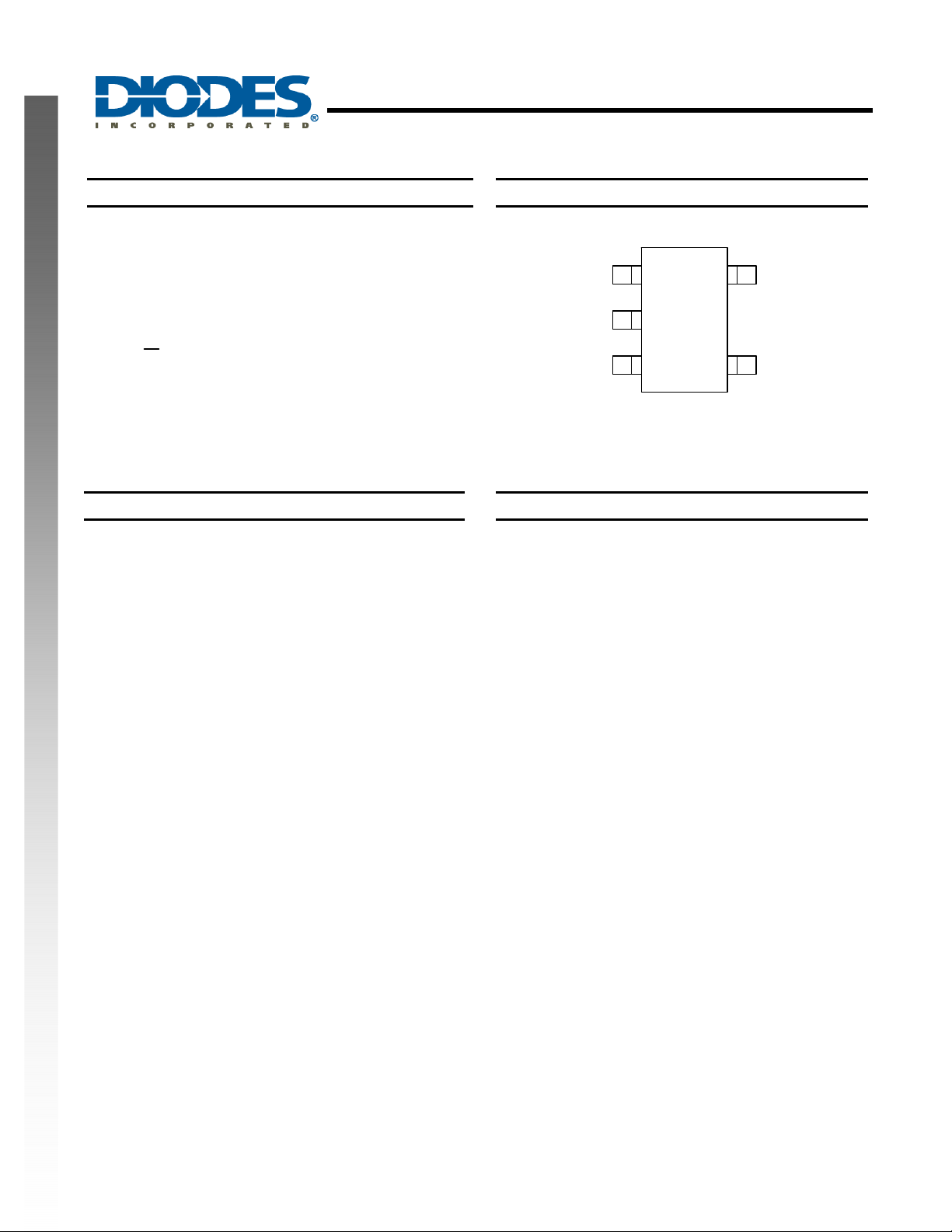
Pin Assignments
AY =
Features
NEW PRODUCT
• Supply Voltage Range from 2.0V to 5.5V
• ± 8 mA Output Drive at 5.0V
• CMOS low power consumption
• Schmitt Trigger Action at Input Makes the Circuit
Tolerant for Slower Input Rise and Fall Time
• ESD Protection per JESD 22
o Exceeds 200-V Machine Model (A115-A)
o Exceeds 2000-V Human Body Model (A114-A)
o Exceeds 1000-V Charged Device Model (C101C)
• Latch-Up Exceeds 100mA per JESD 78, Class II
• SOT25 and SOT353: Assembled with “Green” Molding
Compound (no Br, Sb)
• Lead Free Finish / RoHS Compliant (Note 1)
Notes: 1. EU Directive 2002/95/EC (RoHS). All applicable RoHS exemptions applied. Please visit our website at
http://www.diodes.com/products/lead_free.html.
Applications
• General Purpose Logic
• Wide array of products such as:
o PCs, networking, notebooks, netbooks, PDAs
o Computer peripherals, hard drives, CD/DVD ROM
o TV, DVD, DVR, set top box
o Personal Navigation / GPS
o MP3 players ,Cameras, Video Recorders
NC
A
GND
(Top View)
1
2
SOT25 / SOT353
Vcc
5
Y
43
74AHC1G04
Document number: DS35171 Rev. 1 - 2
1 of 8
www.diodes.com
March 2011
© Diodes Incorporated

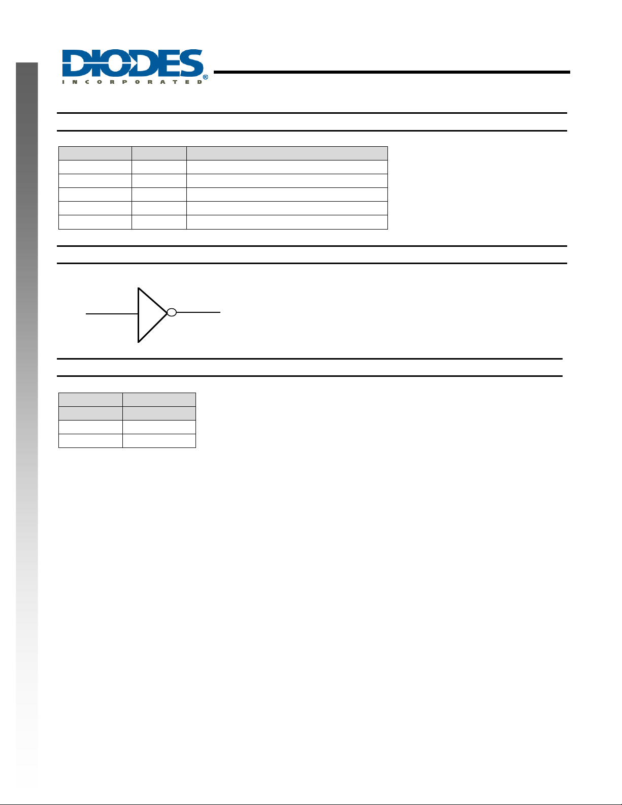
Pin Descriptions
Pin Name Pin NO. Description
NC 1 No Connection
GND 3 Ground
VCC
Logic Diagram
NEW PRODUCT
Function Table
A
2
A 2 Data Input
Y 4 Data Output
5
Supply Voltage
4
Y
74AHC1G04
SINGLE INVERTER GATE
Inputs Output
A Y
H L
L H
74AHC1G04
Document number: DS35171 Rev. 1 - 2
2 of 8
www.diodes.com
March 2011
© Diodes Incorporated

74AHC1G04
SINGLE INVERTER GATE
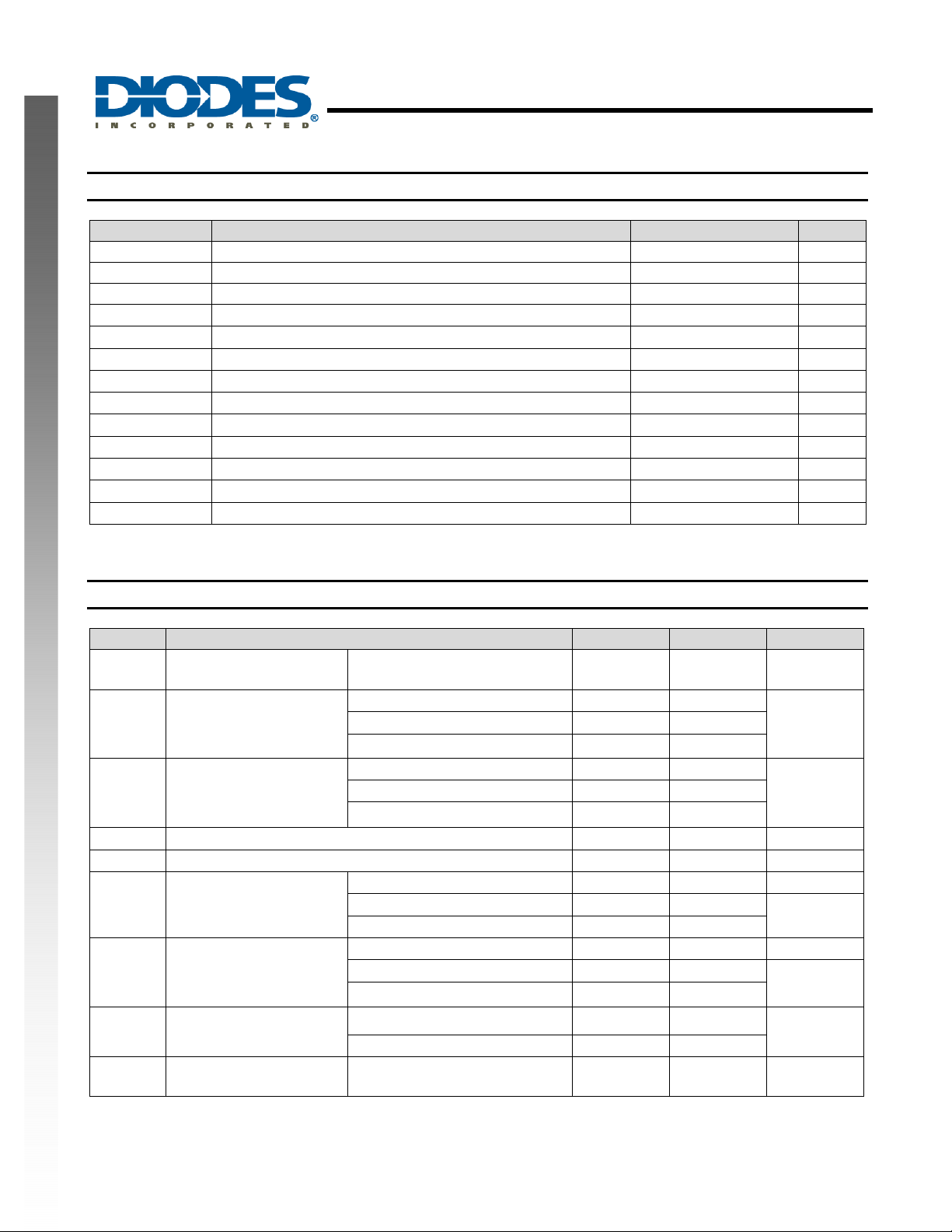
Absolute Maximum Ratings (Note 2)
Symbol Description Rating Unit
ESD HBM Human Body Model ESD Protection 2 KV
ESD CDM Charged Device Model ESD Protection 1 KV
ESD MM Machine Model ESD Protection 200 V
VCC
VI
Vo
IIK Input Clamp Current VI<0
IOK Output Clamp Current (VO < 0 or VO > VCC)
IO Continuo us output current (VO = 0 to VCC)
ICC Continuous current through VCC
I
GND
TJ
T
STG
Notes: 2. Stresses beyond the absolute maximum may result in immediate failure or reduced reliability. These are stre ss values and device operation should
be within recommend values.
NEW PRODUCT
Supply Voltage Range -0.5 to 6.5 V
Input Voltage Range -0.5 to 6.5 V
Voltage applied to output in high or low state
Continuous current through GND -50 mA
Operating Junction Temperature -40 to 150 °C
Storage Temperature -65 to 150 °C
-0.5 to VCC +0.5
-20 mA
±20 mA
±25 mA
50 mA
V
Recommended Operating Conditions (Note 3)
Symbol Parameter Min Max Unit
VCC
V
VIL
VI
VO
IOH
IOL
Δt/ΔV
TA
Notes: 3. Unused inputs should be held at VCC or Ground.
Operating Voltage
High-level Input Voltage
IH
Low-level input voltage
Input Voltage 0 5.5 V
Output Voltage 0
High-level output current
Low-level output current
Input transition rise or fall
rate
Operating free-air
temperature
= 2V
V
CC
VCC = 3V
VCC = 5.5V
= 2V
V
CC
VCC = 3V
VCC = 5.5V
= 2V
V
CC
VCC = 3.3V ± 0.3V
VCC = 5V ± 0.5V
VCC = 2V
VCC = 5V ± 0.5V
VCC = 3V
= 3.3V ± 0.3V
V
CC
VCC = 5V ± 0.5V
2 5.5 V
1.5
2.1
3.85
0.5
0.9
1.65
VCC
-50 uA
-4
-8
50 uA
4
8
100
20
-40 125 ºC
74AHC1G04
Document number: DS35171 Rev. 1 - 2
3 of 8
www.diodes.com
March 2011
© Diodes Incorporated
V
V
V
mA
mA
ns/V
 Loading...