

Page 1
R
Features
• BV
• Max Continuous Current I
• Epitaxial Planar Die Construction
• Complementary PNP Type Available (2DB1132)
• Ideally Suited for Automated Assembly Processes
• Ideal for Medium Power Switching or Amplification Applications
• Totally Lead-Free & Fully RoHS compliant (Notes 1 & 2)
• Halogen and Antimony Free. “Green” Device (Note 3)
• Qualified to AEC-Q101 Standards for High Reliability
CEO
> 32V
= 1A
C
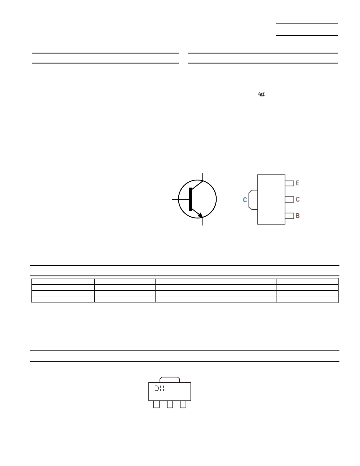
SOT89
B
Top View Device Symbol Pin Out – Top View
2DD1664P/Q/
32V NPN SUFACE MOUNT TRANSISTOR IN SOT89
Mechanical Data
• Case: SOT89
• Case Material: Molded Plastic. “Green” Molding Compound.
• UL Flammability Rating 94V-0
• Moisture Sensitivity: Level 1 per J-STD-020
• Terminals: Matte Tin Finish
• Weight: 0.055 grams (Approximate)
C
E
Ordering Information (Note 4)
Product Marking Reel size (inches) Tape width (mm) Quantity per reel
2DD1664P-13 N13P 13 12 2,500
2DD1664Q-13 N13Q 13 12 2,500
2DD1664R-13 N13R 13 12 2,500
Notes: 1. No purposely added lead. Fully EU Directive 2002/95/EC (RoHS) & 2011/65/EU (RoHS 2) compliant.
3. Halogen and Antimony free "Green” products are defined as those which contain <900ppm bromine, <900ppm chlorine (<1500ppm total Br + Cl) and
4. For packaging details, go to our website at http://www.diodes.com
2. See http://www.diodes.com for more information about Diodes Incorporated’s definitions of Halogen and Antimony free,"Green" and Lead-Free.
<1000ppm antimony compounds.
Marking Information
2DD1664P/Q/R
Document number: DS31143 Rev. 5 - 2
YWW
N13x
1 of 6
www.diodes.com
N13x = Product Type Marking Code:
Where N13P = 2DD1664P
N13Q = 2DD1664Q
N13R = 2DD1664R
YWW = Date Code Marking
Y = Last digit of year ex: 1 = 2011
WW = Week code (01 – 53)
© Diodes Incorporated
July 2012
Page 2
R
P, P
OWER
PATIO
N
Maximum Ratings (@T
Characteristic Symbol Value Unit
Collector-Base Voltage
Collector-Emitter Voltage
Emitter-Base Voltage
Continuous Collector Current
Peak Pulse Current (Note 6)
= +25°C, unless otherwise specified.)
A
V
CBO
V
CEO
V
EBO
I
C
I
CM
40 V
32 V
6 V
1 A
2 A
2DD1664P/Q/
Thermal Characteristics
Characteristic Symbol Value Unit
Power Dissipation (Note 5)
Thermal Resistance, Junction to Ambient (Note 5)
Thermal Resistance, Junction to Leads (Note 7)
Operating and Storage Temperature Range
Notes: 5. For a device surface mounted on FR-4 PCB with minimum suggested pad layout; high coverage of single sided 1 oz copper, in still air conditions
6. Measured under pulsed conditions. Pulse width = 300µs. Duty cycle ≤ 2%.
7. Thermal resistance from junction to solder-point (at the end of the collector lead).
P
R
R
T
J, TSTG
D
θJA
θJL
1 W
125
22
-55 to +150
°C/W
°C/W
1.0
°C
0.8
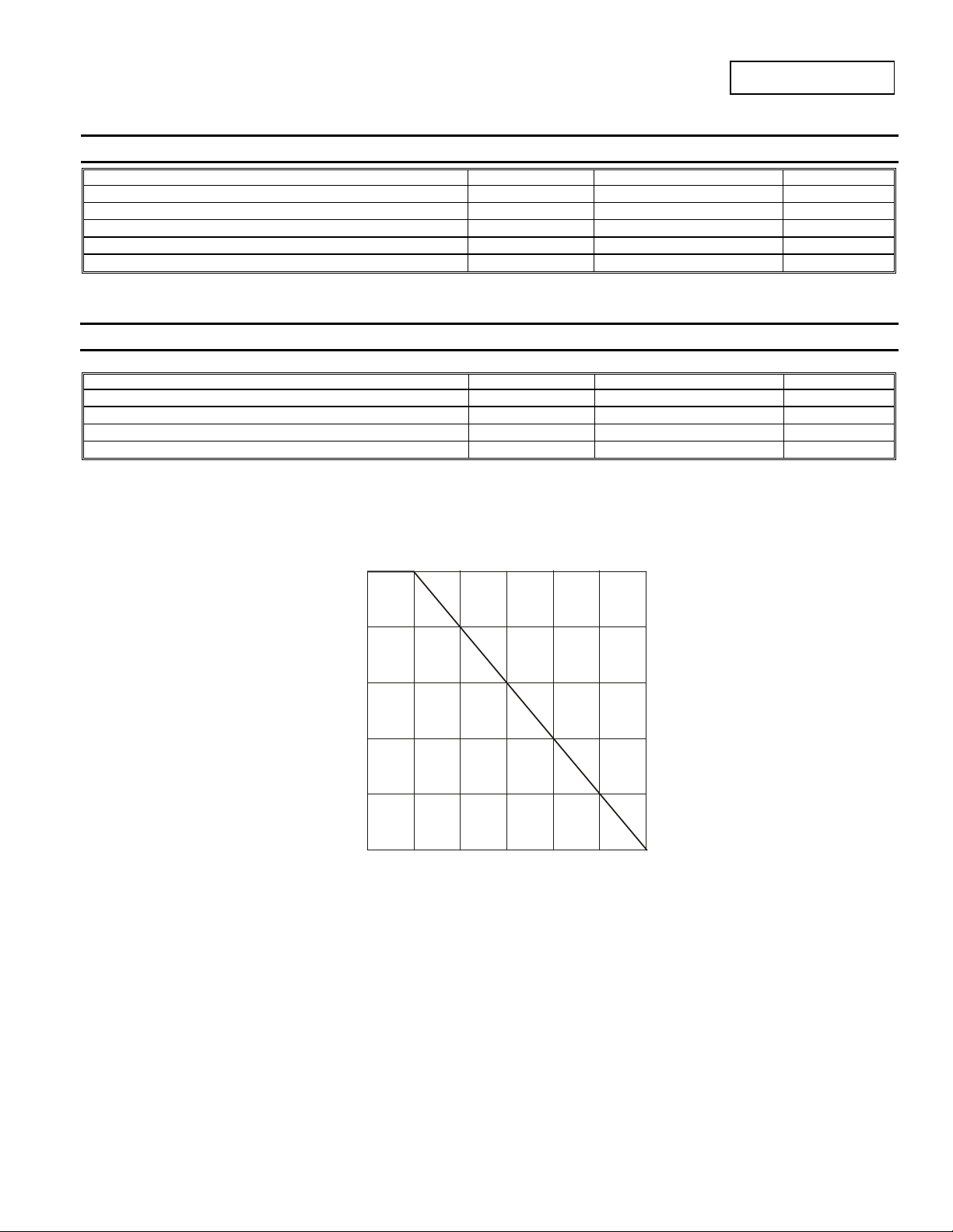
(W)
0.6
DISSI
0.4
D
0.2
0
0
25 50
T , AMBIENT TEMPERATURE (°C)
Figur e 1. Power Dissi pation vs. Ambie nt Temperatur e
A
75 100 125
150
2DD1664P/Q/R
Document number: DS31143 Rev. 5 - 2
2 of 6
www.diodes.com
July 2012
© Diodes Incorporated
Page 3

R
)
Electrical Characteristics (@T
= +25°C, unless otherwise specified.)
A
Characteristic Symbol Min Typ Max Unit Test Condition
Collector-Base Breakdown Voltage
Collector-Emitter Breakdown Voltage (Note 8)
Emitter-Base Breakdown Voltage
Collector-Emitter Cut-off Current
Collector-Base Cut-off Current
Base-Emitter Cut-off Current
Static Forward Current Transfer
Ratio (Note 8)
2DD1664P
2DD1664Q 120 270
2DD1664R 180 390
Collector-Emitter saturation Voltage (Note 8)
Transition frequency
Output Capacitance
Notes: 8. Measured under pulsed conditions. Pulse width = 300µs. Duty cycle ≤ 2%
Electrical Characteristics (@T
= +25°C, unless otherwise specified.)
A
BV
BV
BV
I
I
I
V
CE(sat
CES
CBO
EBO
h
f
C
CBO
CEO
EBO
FE
T
ob
1.8
1.6
40
32
6
- - 100 nA
- - 100 nA
- - 100 nA
82
- 120 400 mV
- 280 - MHz
- 10 - pF
-
-
-
- V
- V
- V
IC = 100µA
IC = 10mA
IE = 100µA
VCE = 32V
VCB = 36V
VEB = 6V
180
-
-
IC = 100mA, V
IC = 500mA, IB = 50mA
IE = 50mA, VCE = 5V, f = 30MHz
IE = 0A, V
400
2DD1664P/Q/
= 3V
CE
= 10V, f = 1MHz
CB
V = 3V
CE
1.4
1.2
300
T = 150°C
A
T = 85°C
A
1.0
T = 25°C
0.8
200
A
0.6
T = -55°C
0.4
100
A
0.2
0
2DD1664P/Q/R
Document number: DS31143 Rev. 5 - 2
3 of 6
www.diodes.com
0
0.001 0.01 0.1 1 10
July 2012
© Diodes Incorporated
Page 4

R
Electrical Characteristics (cont.) (@T
I/I = 10
CB
T = 150°C
A
T = 85°C
A
= +25°C, unless otherwise specified.)
A
T = 25°C
A
T = -55°C
A
40
T = -55°C
A
T = 25°C
A
T = 85°C
A
T = 150°C
A
2DD1664P/Q/
V = 3V
CE
T = -55°C
A
T = 25°C
A
T = 85°C
A
T = 150°C
A
I/I = 10
CB
30
20
10
0
V = 5V
CE
f = 100MHz
-I , EMITTER CURRENT
E
Figure 8 . Typ ical Gain-Bandwid t h Produc t vs . Emitter Current
2DD1664P/Q/R
Document number: DS31143 Rev. 5 - 2
4 of 6
www.diodes.com
July 2012
© Diodes Incorporated
Page 5

R
Package Outline Dimensions
E
B1
D1
e
8° (4X)
D
0
0
2
.
0
R
1
H
L
B
Suggested Pad Layout
Y3
Y
X (3x)
X1
X2 (2x)
Y4
Y2
C
2DD1664P/Q/
C
Dim Min Max
H
A
A 1.40 1.60
B 0.44 0.62
B1 0.35 0.54
C 0.35 0.44
D 4.40 4.60
D1 1.62 1.83
H 3.94 4.25
H1 2.63 2.93
Dimensions Value (in mm)
Y1
SOT89
E 2.29 2.60
e 1.50 Typ
L 0.89 1.20
All Dimensions in mm
X 0.900
X1 1.733
X2 0.416
Y 1.300
Y1 4.600
Y2 1.475
Y3 0.950
Y4 1.125
C 1.500
2DD1664P/Q/R
Document number: DS31143 Rev. 5 - 2
5 of 6
www.diodes.com
July 2012
© Diodes Incorporated
Page 6

R
IMPORTANT NOTICE
DIODES INCORPORATED MAKES NO WARRANTY OF ANY KIND, EXPRESS OR IMPLIED, WITH REGARDS TO THIS DOCUMENT,
INCLUDING, BUT NOT LIMITED TO, THE IMPLIED WARRANTIES OF MERCHANTABILITY AND FITNESS FOR A PARTICULAR PURPOSE
(AND THEIR EQUIVALENTS UNDER THE LAWS OF ANY JURISDICTION).
Diodes Incorporated and its subsidiaries reserve the right to make modifications, enhancements, improvements, corrections or other changes
without further notice to this document and any product described herein. Diodes Incorporated does not assume any liability arising out of the
application or use of this document or any product described herein; neither does Diodes Incorporated convey any license under its patent or
trademark rights, nor the rights of others. Any Customer or user of this document or products described herein in such applications shall assume
all risks of such use and will agree to hold Diodes Incorporated and all the companies whose products are represented on Diodes Incorporated
website, harmless against all damages.
Diodes Incorporated does not warrant or accept any liability whatsoever in respect of any products purchased through unauthorized sales channel.
Should Customers purchase or use Diodes Incorporated products for any unintended or unauthorize d application, Customers shall indemnify and
hold Diodes Incorporated and its representatives harmless against all claims, damages, expenses, and attorney fees arising out of, directly or
indirectly, any claim of personal injury or death associated with such unintended or unauthorized application.
Products described herein may be covered by one or more United States, international or foreign patents pending. Product names and markings
noted herein may also be covered by one or more United States, international or foreign trademarks.
LIFE SUPPORT
Diodes Incorporated products are specifically not authorized for use as critical components in life support devices or systems without the express
written approval of the Chief Executive Officer of Diodes Incorporated. As used herein:
A. Life support devices or systems are devices or systems which:
1. are intended to implant into the body, or
2. support or sustain life and whose failure to perform when properly used in accordance with instructions for use provided in the
labeling can be reasonably expected to result in significant injury to the user.
B. A critical component is any component in a life support device or system whose failure to perform can be reasonably expected to cause the
failure of the life support device or to affect its safety or effectiveness.
Customers represent that they have all necessary expertise in the safety and regulatory ramifications of their life support devices or systems, and
acknowledge and agree that they are solely responsible for all legal, regulatory and safety-related requirements concerning their products and any
use of Diodes Incorporated products in such safety-critical, life support devices or systems, notwithstanding any devices- or systems-related
information or support that may be provided by Diodes Incorporated. Further, Customers must fully indemnify Diodes Incorporated and its
representatives against any damages arising out of the use of Diodes Incorporated products in such safety-critical, life support devices or systems.
Copyright © 2012, Diodes Incorporated
www.diodes.com
2DD1664P/Q/
2DD1664P/Q/R
Document number: DS31143 Rev. 5 - 2
6 of 6
www.diodes.com
July 2012
© Diodes Incorporated
 Loading...