

Page 1
Features
• Ultra-Small Leadless Surface Mount Package
• Complementary PNP Type Available (2DA1774QLP)
• “Lead Free”, RoHS Compliant (Note 1)
• Halogen and Antimony Free, "Green" Device (Note 2)
• Qualified to AEC-Q101Standards for High Reliability
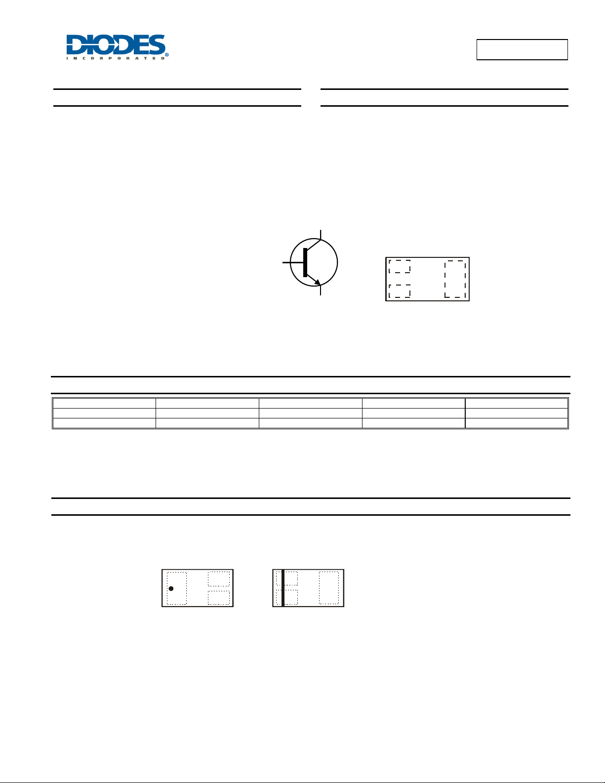
DFN1006-3
Bottom View
2DC4617QLP
50V NPN SMALL SIGNAL SURFACE MOUNT TRANSISTOR
Mechanical Data
• Case: DFN1006-3
• Case Material: Molded Plastic, "Green" Molding Compound. UL
Flammability Classification Rating 94V-0
• Moisture Sensitivity: Level 1 per J-STD-020
• Terminals: Finish ⎯ NiPdAu over Copper leadframe. Solderable
per MIL-STD-202, Method 208
• Weight: 0.0008 grams (approximate)
C
B
E
Device Symbol
B
C
E
Top View
Device Schematic
Ordering Information (Note 3)
Product Marking Reel size (inches) Tape width (mm) Quantity per reel
2DC4617QLP-7 8D 7 8 3,000
2DC4617QLP-7B 8D 7 8 10,000
Notes: 1. No purposefully added lead.
2. Diodes Inc's "Green" policy can be found on our website at http://www.diodes.com.
3. For packaging details, go to our website at http://www.diodes.com.
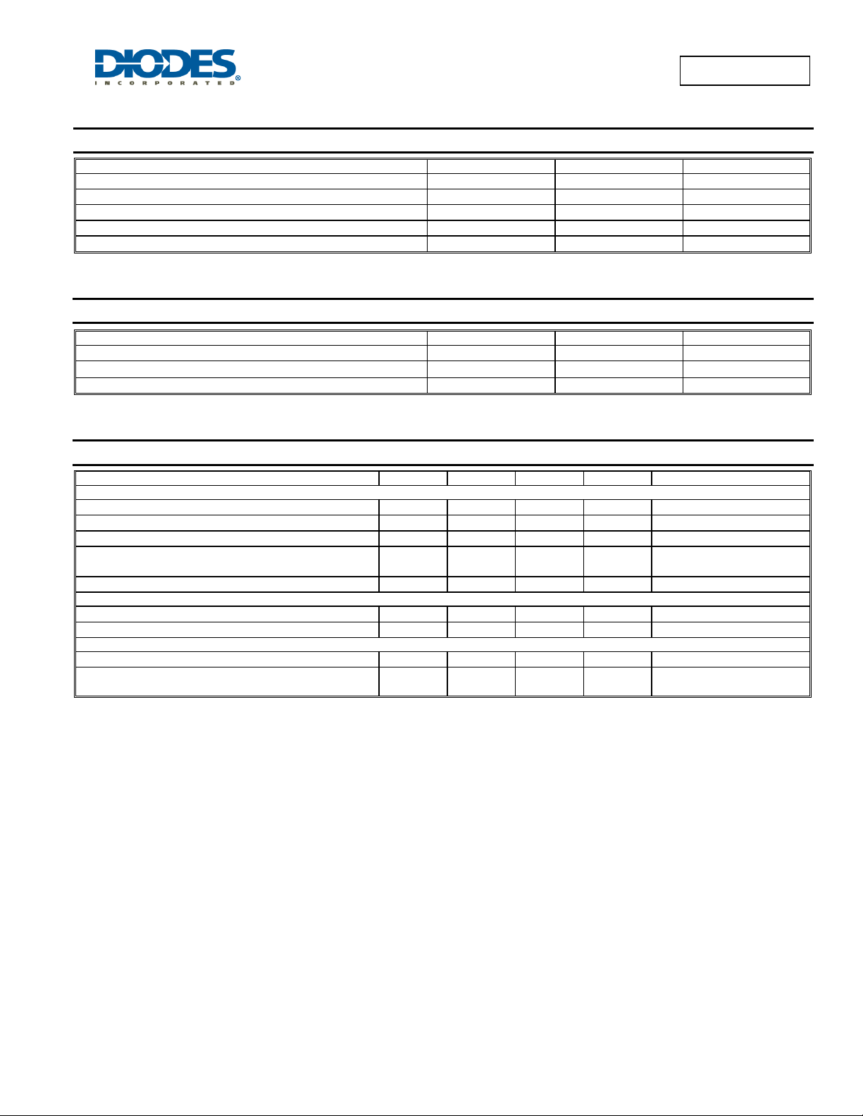
Marking Information
2DC4617QLP
Document number: DS31439 Rev. 4 - 2
2DC4617QLP-7 2DC4617QLP-7B
8D8D
Top View
Dot Denotes
Collector Side
Top View
Bar Denotes Base
and Emitter Side
1 of 5
www.diodes.com
8D = Product Type Marking Code
February 2011
© Diodes Incorporated
Page 2
θ
(BR)
(BR)
(BR)
)
2DC4617QLP
Maximum Ratings @T
= 25°C unless otherwise specified
A
Characteristic Symbol Value Unit
Collector-Base Voltage
Collector-Emitter Voltage
Emitter-Base Voltage
Collector Current - Continuous
Peak Collector Current
V
CBO
V
CEO
V
EBO
I
C
I
CM
50 V
50 V
5.0 V
100 mA
200 mA
Thermal Characteristics @T
= 25°C unless otherwise specified
A
Characteristic Symbol Value Unit
Power Dissipation (Note 4)
Thermal Resistance, Junction to Ambient (Note 4)
Operating and Storage Temperature Range
P
D
R
JA
T
, T
J
STG
250 mW
500
-55 to +150
°C/W
°C
Electrical Characteristics @T
= 25°C unless otherwise specified
A
Characteristic Symbol Min Max Unit Test Condition
OFF CHARACTERISTICS (Note 5)
Collector-Base Breakdown Voltage
Collector-Emitter Breakdown Voltage
Emitter-Base Breakdown Voltage
Collector Cutoff Current
Emitter Cutoff Current
V
V
V
I
CBO
I
EBO
CBO
CEO
EBO
⎯
50
50
5.0
⎯
⎯
⎯
100
5
⎯
100 nA
V
V
V
nA
μA
IC = 50μA, IE = 0
IC = 1.0mA, IB = 0
IE = 50μA, IC = 0
= 30V
V
CB
= 30V, TA = 150°C
V
CB
V
= 4.0V
EB
ON CHARACTERISTICS (Note 5)
DC Current Gain
Collector-Emitter Saturation Voltage
h
V
CE(SAT
FE
120 270
⎯
⎯ VCE = 6.0V, IC = 1.0mA
0.2 V
IC = 50mA, IB = 5.0mA
SMALL SIGNAL CHARACTERISTICS
Output Capacitance
Current Gain-Bandwidth Product
Notes: 4. Part mounted on FR-4 PCB with recommended pad layout.
5. Short duration pulse test used to minimize self-heating effect.
C
⎯
obo
f
T
100
3.5 pF
⎯
MHz
VCB = 12V, f = 1.0MHz, IE = 0
V
CE
f = 100MHz
= 12V, IC = 2.0mA,
2DC4617QLP
Document number: DS31439 Rev. 4 - 2
2 of 5
www.diodes.com
February 2011
© Diodes Incorporated
Page 3

P, P
OWER
P
TIO
C
O
CTO
R CUR
R
T
C CUR
REN
T GAIN
C
O
CTO
R
T
TER
5
T
TER TUR
N
O
N VOLT
G
2DC4617QLP
300
250
N (mW)
200
A
100
(mA)
EN
80
60
I = 0.5mA
B
I = 0.4mA
B
I = 0.3mA
B
150
DISSI
100
D
50
R = 500 C/W
°
θ
JA
0
0 255075100125150
T , AMBIENT TEMPERATURE (°C)
A
Fig. 1 Power Derating Curve
400
40
LLE
20
C
I,
0
012 345
V , COLLECTOR-EMIT TER VOLTAGE (V)
CE
Fig. 2 Typical Collector Current
vs. Collector-Emitter Voltage
0.
0.4
I/I = 10
CB
I = 0.2mA
B
I = 0.1mA
B
300
-EMI
0.3
200
LLE
FE
100
h, D
0
0.1 1 10 100 1,000
I , COLLECTOR CURRENT (mA)
C
Typical DC Current Gain
Fig. 3
vs. Collector Current
1.2
0.2
SATURATION VO LTAGE (V)
0.1
CE(SAT)
V,
0
0.1 1 10 100 1,000
I , COLLECTOR CURRENT (mA)
C
Typical Collector-Emitter Saturation Voltage
Fig. 4
vs. Collecto r Cu r re nt
1.2
T = 150ºC
A
T = 85ºC
A
T = -55ºC
A
T = 25ºC
A
E (V)
A
1.0
0.8
-
0.6
0.4
0.2
BE(ON)
0
V , BASE-EMI
0.1 1 10 100 1,000
I , COLLECTOR CURRENT (mA)
C
Ty pi cal Base-E mitter Turn-On Voltage
Fig. 5
vs. Collector Current
1.0
0.8
T = -55°C
A
0.6
T = 25°C
A
T = 85°C
0.4
BE(SAT)
V , BASE-EMITTER
SATURATION VOLT AGE (V)
0.2
A
T = 150°C
A
0
0.1 1 10 100
I , COLLECTOR CURRENT (mA)
C
Fig. 6 Typical Base-Emitter Saturation Voltage
vs. Collector Current
I/I = 10
CB
1,000
2DC4617QLP
Document number: DS31439 Rev. 4 - 2
3 of 5
www.diodes.com
February 2011
© Diodes Incorporated
Page 4

Package Outline Dimensions
A
A1
D
b2
E
L2
Suggested Pad Layout
X
1
G2
X
Y
2DC4617QLP
Document number: DS31439 Rev. 4 - 2
2DC4617QLP
DFN1006-3
Dim Min Max Typ
A 0.47 0.53 0.50
A1 0 0.05 0.03
b1 0.10 0.20 0.15
b2 0.45 0.55 0.50
D 0.95 1.075 1.00
b1
e
L1L3
C
Dimensions Value (in mm)
G1
Z
4 of 5
www.diodes.com
E 0.55 0.675 0.60
e
⎯ ⎯
L1 0.20 0.30 0.25
L2 0.20 0.30 0.25
L3
⎯ ⎯
All Dimensions in mm
Z 1.1
G1 0.3
G2 0.2
X 0.7
X1 0.25
Y 0.4
C 0.7
0.35
0.40
February 2011
© Diodes Incorporated
Page 5

IMPORTANT NOTICE
DIODES INCORPORATED MAKES NO WARRANTY OF ANY KIND, EXPRESS OR IMPLIED, WITH REGARDS TO THIS DOCUMENT,
INCLUDING, BUT NOT LIMITED TO, THE IMPLIED WARRANTIES OF MERCHANTABILITY AND FITNESS FOR A PARTICULAR PURPOSE
(AND THEIR EQUIVALENTS UNDER THE LAWS OF ANY JURISDICTION).
Diodes Incorporated and its subsidiaries reserve the right to make modifications, enhancements, improvements, corrections or other changes
without further notice to this document and any product described herein. Diodes Incorporated does not assume any liability arising out of the
application or use of this document or any product described herein; neither does Diodes Incorporated convey any license under its patent or
trademark rights, nor the rights of others. Any Customer or user of this document or products described herein in such applications shall assume
all risks of such use and will agree to hold Diodes Incorporated and all the companies whose products are represented on Diodes Incorporated
website, harmless against all damages.
Diodes Incorporated does not warrant or accept any liability whatsoever in respect of any products purchased through unauthorized sales channel.
Should Customers purchase or use Diodes Incorporated products for any unintended or unauthorize d application, Customers shall indemnify and
hold Diodes Incorporated and its representatives harmless against all claims, damages, expenses, and attorney fees arising out of, directly or
indirectly, any claim of personal injury or death associated with such unintended or unauthorized application.
Products described herein may be covered by one or more United States, international or foreign patents pending. Product names and markings
noted herein may also be covered by one or more United States, international or foreign trademarks.
LIFE SUPPORT
Diodes Incorporated products are specifically not authorized for use as critical components in life support devices or systems without the express
written approval of the Chief Executive Officer of Diodes Incorporated. As used herein:
A. Life support devices or systems are devices or systems which:
1. are intended to implant into the body, or
2. support or sustain life and whose failure to perform when properly used in accordance with instructions for use provided in the
labeling can be reasonably expected to result in significant injury to the user.
B. A critical component is any component in a life support device or system whose failure to perform can be reasonably expected to cause the
failure of the life support device or to affect its safety or effectiveness.
Customers represent that they have all necessary expertise in the safety and regulatory ramifications of their life support devices or systems, and
acknowledge and agree that they are solely responsible for all legal, regulatory and safety-related requirements concerning their products and any
use of Diodes Incorporated products in such safety-critical, life support devices or systems, notwithstanding any devices- or systems-related
information or support that may be provided by Diodes Incorporated. Further, Customers must fully indemnify Diodes Incorporated and its
representatives against any damages arising out of the use of Diodes Incorporated products in such safety-critical, life support devices or systems.
Copyright © 2011, Diodes Incorporated
www.diodes.com
2DC4617QLP
2DC4617QLP
Document number: DS31439 Rev. 4 - 2
5 of 5
www.diodes.com
February 2011
© Diodes Incorporated
 Loading...