

Page 1
Please click here to visit our online spice models database.
Features
• Epitaxial Planar Die Construction
• Ideally Suited for Automated Assembly Processes
• Ideal for Medium Power Switching or Amplification Applications
• Lead Free By Design/RoHS Compliant (Note 1)
• "Green" Device (Note 2)
2DB1119S
PNP SURFACE MOUNT TRANSISTOR
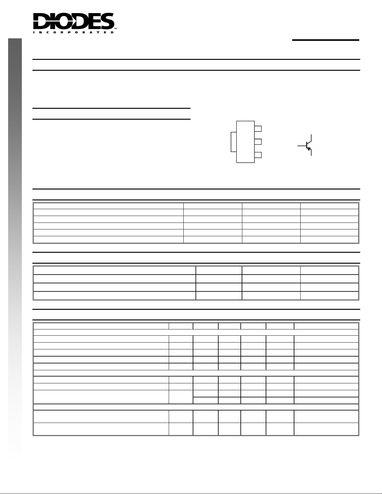
Mechanical Data
• Case: SOT89-3L
• Case Material: Molded Plastic, "Green” Molding Compound.
UL Flammability Classification Rating 94V-0
• Moisture Sensitivity: Level 1 per J-STD-020C
• Terminals: Finish — Matte Tin annealed over Copper leadframe
NEW PRODUCT
(Lead Free Plating). Solderable per MIL-STD-202, Method 208
• Marking Information: See Page 3
• Ordering Information: See Page 3
• Weight: 0.072 grams (approximate)
Maximum Ratings @T
Characteristic Symbol Value Unit
Collector-Base Voltage
Collector-Emitter Voltage
Emitter-Base Voltage
Peak Pulse Current
Continuous Collector Current
= 25°C unless otherwise specified
A
Thermal Characteristics
Characteristic Symbol Value Unit
Power Dissipation (Note 3) @ TA = 25°C P
Thermal Resistance, Junction to Ambient Air (Note 3) @ TA = 25°C
Operating and Storage Temperature Range
SOT89-3L
T
O
R
L
L
C
E
C
O
E
3
C
C
4
O
T
V
CBO
V
CEO
V
EBO
I
CM
I
C
D
R
JA
θ
T
, T
j
STG
2
B
1
W
E
I
V
P
Schematic and Pin Configuration
-25 V
-25 V
125 °C/W
-55 to +150 °C
B
-5 V
-2 A
-1 A
1 W
2,4
1
E
S
A
3
E
T
I
M
T
E
R
Electrical Characteristics @T
OFF CHARACTERISTICS (Note 4)
Collector-Base Breakdown Voltage
Collector-Emitter Breakdown Voltage
Emitter-Base Breakdown Voltage
Collector Cut-Off Current
Emitter Cut-Off Current
ON CHARACTERISTICS (Note 4)
Collector-Emitter Saturation Voltage
Base-Emitter Saturation Voltage
DC Current Gain
SMALL SIGNAL CHARACTERISTICS
Transition Frequency
Output Capacitance
Notes: 1. No purposefully added lead.
4. Measured under pulsed conditions. Pulse width = 300μs. Duty cycle ≤2%.
DS31298 Rev. 2 - 2
2. Diodes Inc.'s "Green" policy can be found on our website at http://www.diodes.com/products/lead_free/index.php.
3. Device mounted on FR-4 PCB; pad layout as shown on page 4 or in Diodes Inc. suggested pad layout document AP02001, which can be found on our
website at http://www.diodes.com/datasheets/ap02001.pdf.
Characteristic Symbol Min Typ Max Unit Conditions
= 25°C unless otherwise specified
A
V
(BR)CBO
V
(BR)CEO
V
(BR)EBO
I
CBO
I
EBO
V
CE(SAT)
V
BE(SAT)
h
FE
f
T
C
ob
www.diodes.com
-25
-25
-5
⎯ ⎯
⎯ ⎯
⎯
⎯
140
40
⎯
⎯
1 of 4
⎯ ⎯
⎯ ⎯
⎯ ⎯
-0.1
-0.1
-0.15 -0.7 V
-0.85 -1.2 V
⎯
⎯ ⎯ ⎯
200
12
280
⎯
⎯
V
V
V
μA
μA
⎯
MHz
pF
I
= -10μA, IE = 0
C
I
= -1mA, IB = 0
C
I
= -10μA, IC = 0
E
V
= -20V, IE = 0
CB
V
= -4V, IC = 0
EB
I
= -500mA, IB = -50mA
C
I
= -500mA, IB = -50mA
C
V
= -2V, IC = -50mA
CE
V
= -2V, IC = -1A
CE
= -10V, IC = -50mA
V
CE
f = 100MHz
= -10V, IE = 0,
V
CB
f = 1MHz
2DB1119S
© Diodes Incorporated
Page 2
P
P
OWER
P
T
O
1.0
1.2
NEW PRODUCT
0.8
N (W)
I
A
0.6
DISSI
1.0
0.8
0.6
0.4
0.4
,
D
0.2
350
0
25 50 75 100 125 150
0
T , AMBIENT TEMPERATURE ( C)
A
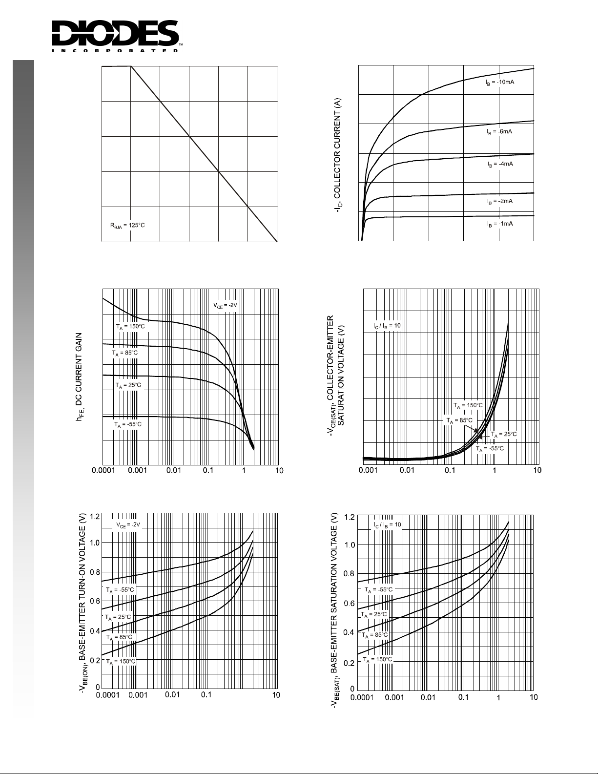
Fig. 1 Power Dissipation
vs. Ambien t T empe rature (Note 3)
°
0.2
0
01 23 45
-V , COLLECTOR-EMITTER VOLTAGE (V)
CE
Fig. 2 Typical Collector Current
vs. Collector-Emitter Voltage
0.8
300
250
0.6
200
0.4
150
100
0.2
50
0
-I , COLLECTOR CURRENT (A)
C
Fig. 3 Typical DC Current Gain
vs. Collector Current
0
,
-I COLLECTOR CURRENT (A)
C
Fig. 4 Typical Collector-Emitter Saturation
Voltage vs. C ollector Cu r r ent
1
-I COLLECTOR CURRENT (A)
,
C
Fig. 5 Typical Base-Emitter Turn-On Voltage
vs. Collector Current
DS31298 Rev. 2 - 2
2 of 4
www.diodes.com
-I COLLECTOR CURRENT (A)
,
C
Fig. 6 Typical Base-Emitter Saturation
Voltage vs. Collector Current
2DB1119S
© Diodes Incorporated
Page 3
C
URRENT G
T
H
PRODUCT
H
150
135
120
z)
(M
250
200
105
90
150
75
60
45
30
100
AIN-BANDWID
50
15
NEW PRODUCT
0
V REVERSE VOLTAGE (V)
,
R
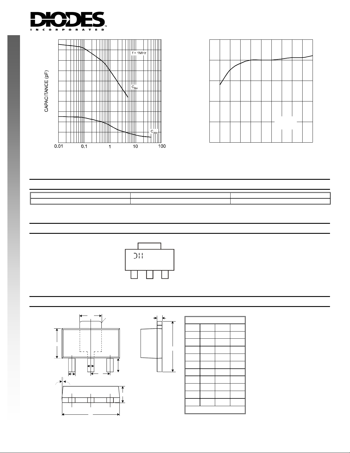
Fig. 7 Typical Capacitance Characteristics
0
T
f,
0102030405060708090100
-I , COLLECTOR CURRENT (mA)
C
Fig. 8 Typical Gain-Bandwidth Pr oduct vs. Collector Current
Ordering Information (Note 5)
Device Packaging Shipping
2DB1119S-13 SOT89-3L 2500/Tape & Reel
Notes: 5. For packaging details, please see below or go to our website at http://www.diodes.com/ap02007.pdf.
Marking Information
(Top View)
P12BS
YWW
P12BS = Product Type Marking Code
YWW = Date Code Marking
Y = Last digit of year ex: 7 = 2007
WW = Week code 01 - 52
V = -10V
CE
f = 100MHz
Package Outline Dimensions
D1
E
B1
8
B
°
(
4
X
)
D
DS31298 Rev. 2 - 2
0
0
2
.
0
R
C
SOT89-3L
Dim Min Max Typ
A 1.40 1.60 1.50
B 0.45 0.55 0.50
H
B1 0.37 0.47 0.42
C 0.35 0.43 0.38
L
e
D 4.40 4.60 4.50
D1 1.50 1.70 1.60
E 2.40 2.60 2.50
e — — 1.50
A
H 3.95 4.25 4.10
L 0.90 1.20 1.05
All Dimensions in mm
3 of 4
www.diodes.com
2DB1119S
© Diodes Incorporated
Page 4

Suggested Pad Layout
1.7
2.7
0.4
1.9
0.9
NEW PRODUCT
Diodes Incorporated and its subsidiaries reserve the right to make modifications, enhancements, improvements, corrections or other changes
without further notice to any product herein. Diodes Incorporated does not assume any liability arising out of the application or use of any product
described herein; neither does it convey any license under its patent rights, nor the rights of others. The user of products in such applications shall
assume all risks of such use and will agree to hold Diodes Incorporated and all the companies whose products are represented on our website,
harmless against all damages.
Diodes Incorporated products are not authorized for use as critical components in life support devices or systems without the expressed written
approval of the President of Diodes Incorporated.
3.0
1.3
Unit: mm
IMPORTANT NOTICE
LIFE SUPPORT
DS31298 Rev. 2 - 2
4 of 4
www.diodes.com
2DB1119S
© Diodes Incorporated
 Loading...