

Page 1
Features
3.0W Power Dissipation
Ideally Suited for Automated Assembly
3.3V - 39V Nominal Zener Voltage Range
Standard V
ESD Rating of Class 3 (>16kV) per Human Body Model
Lead-Free Finish; RoHS Compliant (Notes 1 & 2)
Halogen and Antimony Free. “Green” Device (Note 3)
NEW PRODUCT
Tolerance is ± 5%
Z
Green
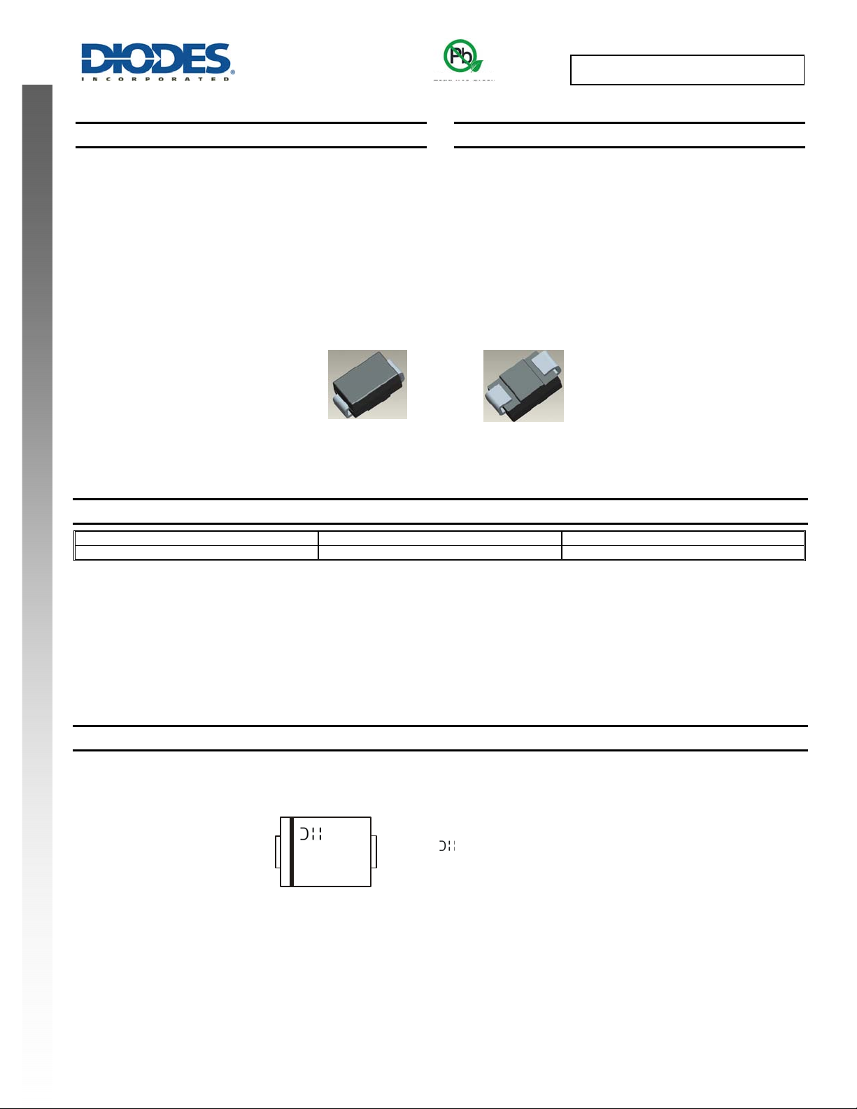
3.0W SURFACE MOUNT POWER ZENER DIODE
Mechanical Data
Case: SMB
Case Material: Molded Plastic. UL Flammability Classification
Rating 94V-0
Moisture Sensitivity: Level 1 per J-STD-020
Terminals: Lead Free Plating (Matte Tin Finish). Solderable per
MIL-STD-202, Method 208
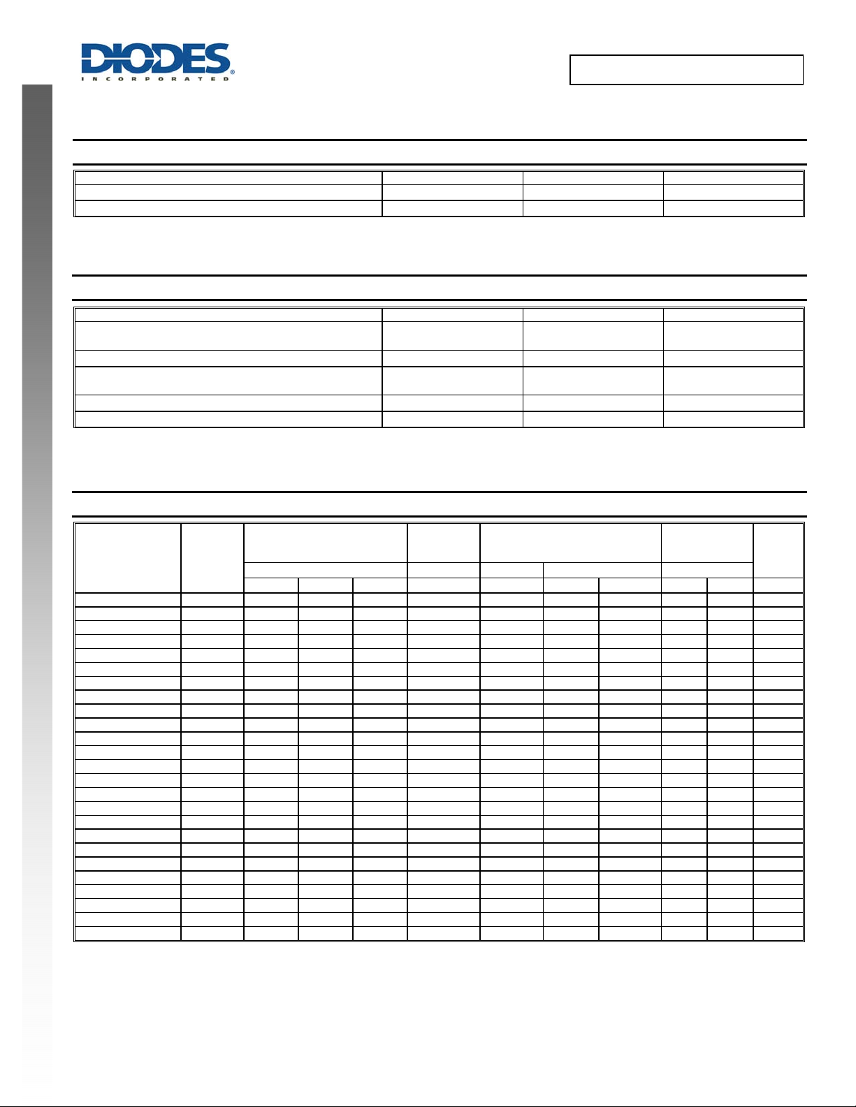
Polarity: Cathode Band
Weight: 0.096 grams (approximate)
Top View Bottom View
1SMB5913B –1SMB5939B
Ordering Information (Note 4)
Device* Packaging Shipping
1SMB59xxB-13 SMB 3000/Tape & Reel
*x = Device Voltage, e.g., 1SMB5920B-13.
Notes: 1. EU Directive 2002/95/EC (RoHS) & 2011/65/EU (RoHS 2) compliant. All applicable RoHS exemptions applied.
2. See http://www.diodes.com/quality/lead_free.html for more information about Diodes Incorporated’s definitions of Halogen- and Antimony-free, "Green"
and Lead-free.
3. Halogen- and Antimony-free "Green” products are defined as those which contain <900ppm bromine, <900ppm chlorine (<1500ppm total Br + Cl) and
<1000ppm antimony compounds.
4. For packaging details, go to our website at http”//www.diodes.com/products/packages.html.
Marking Information
1SMB5913B – 1SMB5939B
Document number: DS32125 Rev. 6 - 2
YWW
B9xx
B9xx = Product Type Marking Code
(See Electric Characteristics Table)
= Manufacturers’ code marking
YWW = Date Code Marking
Y = Last digit of year (ex: 1 for 2011)
WW = Week Code (01 - 53)
1 of 5
www.diodes.com
May 2013
© Diodes Incorporated
Page 2
K
Maximum Ratings (@T
= +25°C, unless otherwise specified.)
A
Characteristic Symbol Value Unit
Forward Voltage @ IF = 200mA VF
Zener Current (see Table page 2)
Thermal Characteristics
Characteristic Symbol Value Unit
Power Dissipation @TL = +75°C
Derate Above +75°C (Note 5)
Thermal Resistance - Junction to Terminal (Note 5)
Power Dissipation @TA = +25°C
Derate Above +25°C (Note 5)
Thermal Resistance - Junction to Ambient (Note 5)
Operating and Storage Temperature Range
NEW PRODUCT
1SMB5913B –1SMB5939B
1.5 V
I
P
ZM
P
D
R
JT
P
D
R
JA
T
J, TSTG
/ VZ
D
3.0
40
25 °C/W
550
4.4
228 °C/W
-65 to +150 °C
mA
W
mW/°C
mW
mW/°C
Electrical Characteristics (@T
Type
Number
Marking
Code
Min (V) Typ (V) Max (V) mA
= +25°C, unless otherwise specified.)
A
Zener Voltage
Range (Note 6)
V
IZT Z
Z @ IZT
Test
Current
Maximum Zener Impedance
(Note 7)
Z
ZT @ IZT
ZK @ IZ
I
mA µA V mA
Maximum
Reverse
Current (Note 6)
VR
R @
I
ZM Max
1SMB5913B B913 3.13 3.3 3.47 113.6 10 500 1 100 1 454
1SMB5914B B914 3.42 3.6 3.78 104.2 9 500 1 75 1 416
1SMB5915B B915 3.7 3.9 4.1 96.1 7.5 500 1 25 1 384
1SMB5916B B916 4.08 4.3 4.52 87.2 6 500 1 5 1 348
1SMB5917B B917 4.46 4.7 4.94 79.8 5 500 1 5 1.5 319
1SMB5920B B920 5.89 6.2 6.51 60.5 2 200 1 5 4 241
1SMB5921B B921 6.46 6.8 7.14 55.1 2.5 200 1 5 5.2 220
1SMB5922B B922 7.12 7.5 7.88 50 3 400 0.5 5 6 200
1SMB5923B B923 7.79 8.2 8.61 45.7 3.5 400 0.5 5 6.5 182
1SMB5924B B924 8.64 9.1 9.56 41.2 4 500 0.5 5 7 164
1SMB5925B B925 9.5 10 10.5 37.5 4.5 500 0.25 5 8 150
1SMB5926B B926 10.45 11 11.55 34.1 5.5 550 0.25 1 8.4 136
1SMB5927B B927 11.4 12 12.6 31.2 6.5 550 0.25 1 9.1 125
1SMB5928B B928 12.35 13 13.65 28.8 7 550 0.25 1 9.9 115
1SMB5929B B929 14.25 15 15.75 25 9 600 0.25 1 11.4 100
1SMB5930B B930 15.2 16 16.8 23.4 10 600 0.25 1 12.2 93
1SMB5931B B931 17.1 18 18.9 20.8 12 650 0.25 1 13.7 83
1SMB5932B B932 19 20 21 18.7 14 650 0.25 1 15.2 75
1SMB5933B B933 20.9 22 23.1 17 17.5 650 0.25 1 16.7 68
1SMB5934B B934 22.8 24 25.2 15.6 19 700 0.25 1 18.2 62
1SMB5935B B935 25.65 27 28.35 13.9 23 700 0.25 1 20.6 55
1SMB5936B B936 28.5 30 31.5 12.5 28 750 0.25 1 22.8 50
1SMB5937B B937 31.35 33 34.65 11.4 33 800 0.25 1 25.1 45
1SMB5938B B938 34.2 36 37.8 10.4 38 850 0.25 1 27.4 41
1SMB5939B B939 37.05 39 40.95 9.6 45 900 0.25 1 29.7 38
Notes: 5. Device mounted on FR-4 PCB; pad layout as shown on Diodes Inc. suggested pad layout document AP02001, which can be found on our website at
specified limits are for I
http://www.diodes.com.
6. Short duration pulse test used to minimize self-heating effect.
7. ZENER IMPEDANCE (ZZ) DERIVATION ZZT and ZZK are measured by dividing the ac voltage drop across the device by the ac current applied. The
Z(AC)
= 0.1 I
with the AC frequency = 60 Hz.
Z(DC)
1SMB5913B – 1SMB5939B
Document number: DS32125 Rev. 6 - 2
2 of 5
www.diodes.com
May 2013
© Diodes Incorporated
Page 3

P
UM P
OWER
PATIO
N
T
C
TEMPERATUR
C
O
F
FICIEN
T
R CUR
RENT
Y
N
C
P
N
C
)
Y
C
P
C
C
TOT
C
P
CITANC
F
NEW PRODUCT
1SMB5913B –1SMB5939B
6
(W)
Note 5
5
40
35
30
4
DISSI
3
T
L
E
25
E
20
15
2
10
Z
1
, MAXIM
D
0
0
T , AMBIENT TEMPERATURE ( C)
A
50
T
A
100
7525
125
°
Figure 1 Power Dissipation vs. Ambient Temperature
100
150
OF ZENER VOLTAGE (mV /°C)
of V ,
5
0
0 5 10 15 20 25 30 35 40
V , ZENER VOLTAGE (V)
Z
Figure 2 Typical Temperature Coefficient of
Zener Voltage vs. Zene r Voltage
1000
15V 39V
10
6.2V 13V
3.3V
(mA)
E (
100
1mA
EDA
IM
1
Z
I, ZENE
0.1
0 1020304050
Figure 3 Typical Char acteristics
V , ZENER VOLTAGE (V)
Z
Zener Breakdown
10
AMI
Z
Z, D
1
110100
V , ZENER VOLTAGE (V)
Figure 4 Effect of Zener Voltage
10mA
20mA
Z
1,800
f = 1MHz
E ( )
EDAN
IM
39V
13V
3.3V
NAMI
Z
Z, D
15V
6.2V
0.1 1 10 100
I , ZENER TEST CURRENT (mA)
Z
Figure 5 Effect of Zener Current
1,600
)
1,400
E (p
1,200
1,000
A
A
800
V = 0V
AL
600
,
400
T
200
0
010203040
/2
V = V
RZ
V , REVERSE VOLTAGE (V)
R
R
Figure 6 Typical Total Capacitance vs. Re verse Voltag e
1SMB5913B – 1SMB5939B
Document number: DS32125 Rev. 6 - 2
3 of 5
www.diodes.com
May 2013
© Diodes Incorporated
Page 4

P, P
P
U
P
OWER
NEW PRODUCT
1SMB5913B –1SMB5939B
100
Peak Value I
Half Value I /2
pp
pp
Peak Value I
pp
Half Value I /2
pp
50
Ppp
PppP
I , PEAK PULSE CURRENT (%I )
0
0
8x20 Waveform
as defined by R.E.A.
20 40
t, TIME ( s)
60
Figur e 7 Pul s e Waveform
10
I , PEAK PULSE CURRENT (%I )
10 X 1000 Waveform
as defined by R.E.A.
t, TIME (ms)
Figure 8 Pulse Waveform
(kW)
1
LSE
EAK
0.1
PK
0.01
0.01 0.1 1 10
t , PULSE DURATION (ms)
d
Figure 9 Max. Peak Pulse Power vs. Pulse Duration
Package Outline Dimensions
Please see AP02002 at http://www.diodes.com/datasheets/ap02002.pdf for latest version.
1SMB5913B – 1SMB5939B
Document number: DS32125 Rev. 6 - 2
A
J
H
B
SMB
Dim Min Max
C
A 3.30 3.94
B 4.06 4.57
C 1.96 2.21
D 0.15 0.31
D
E 5.00 5.59
G 0.05 0.20
H 0.76 1.52
J 2.00 2.50
All Dimensions in mm
G
E
4 of 5
www.diodes.com
May 2013
© Diodes Incorporated
Page 5

1SMB5913B –1SMB5939B
Suggested Pad Layout
Please see AP02002 at http://www.diodes.com/datasheets/ap02002.pdf for latest version.
NEW PRODUCT
DIODES INCORPORATED MAKES NO WARRANTY OF ANY KIND, EXPRESS OR IMPLIED, WITH REGARDS TO THIS DOCUMENT,
INCLUDING, BUT NOT LIMITED TO, THE IMPLIED WARRANTIES OF MERCHANTABILITY AND FITNESS FOR A PARTICULAR PURPOSE
(AND THEIR EQUIVALENTS UNDER THE LAWS OF ANY JURISDICTION).
Diodes Incorporated and its subsidiaries reserve the right to make modifications, enhancements, improvements, corrections or other changes
without further notice to this document and any product described herein. Diodes Incorporated does not assume any liability arising out of the
application or use of this document or any product described herein; neither does Diodes Incorporated convey any license under its patent or
trademark rights, nor the rights of others. Any Customer or user of this document or products described herein in such applications shall assume
all risks of such use and will agree to hold Diodes Incorporated and all the companies whose products are represented on Diodes Incorporated
website, harmless against all damages.
Diodes Incorporated does not warrant or accept any liability whatsoever in respect of any products purchased through unauthorized sales channel.
Should Customers purchase or use Diodes Incorporated products for any unintended or unauthorize d application, Customers shall indemnify and
hold Diodes Incorporated and its representatives harmless against all claims, damages, expenses, and attorney fees arising out of, directly or
indirectly, any claim of personal injury or death associated with such unintended or unauthorized application.
Products described herein may be covered by one or more United States, international or foreign patents pending. Product names and markings
noted herein may also be covered by one or more United States, international or foreign trademarks.
This document is written in English but may be translated into multiple languages for reference. Onl y the English version of this document is the
final and determinative format released by Diodes Incorporated.
Diodes Incorporated products are specifically not authorized for use as critical components in life support devices or systems without the express
written approval of the Chief Executive Officer of Diodes Incorporated. As used herein:
A. Life support devices or systems are devices or systems which:
1. are intended to implant into the body, or
labeling can be reasonably expected to result in significant injury to the user.
B. A critical component is any component in a life support device or system whose failure to perform can be reasonably expected to cause the
failure of the life support device or to affect its safety or effectiveness.
Customers represent that they have all necessary expertise in the safety and regulatory ramifications of their life support devices or systems, and
acknowledge and agree that they are solely responsible for all legal, regulatory and safety-related requirements concerning their products and any
use of Diodes Incorporated products in such safety-critical, life support devices or systems, notwithstanding any devices- or systems-related
information or support that may be provided by Diodes Incorporated. Further, Customers must fully indemnify Diodes Incorporated and its
representatives against any damages arising out of the use of Diodes Incorporated products in such safety-critical, life support devices or systems.
Copyright © 2013, Diodes Incorporated
www.diodes.com
2. support or sustain life and whose failure to perform when properly used in accordance with instructions for use provided in the
X
Y
1SMB5913B – 1SMB5939B
Document number: DS32125 Rev. 6 - 2
C
Dimensions Value (in mm)
Z 6.8
G 1.8
X 2.3
Y 2.5
G
Z
IMPORTANT NOTICE
LIFE SUPPORT
5 of 5
www.diodes.com
C 4.3
© Diodes Incorporated
May 2013
 Loading...