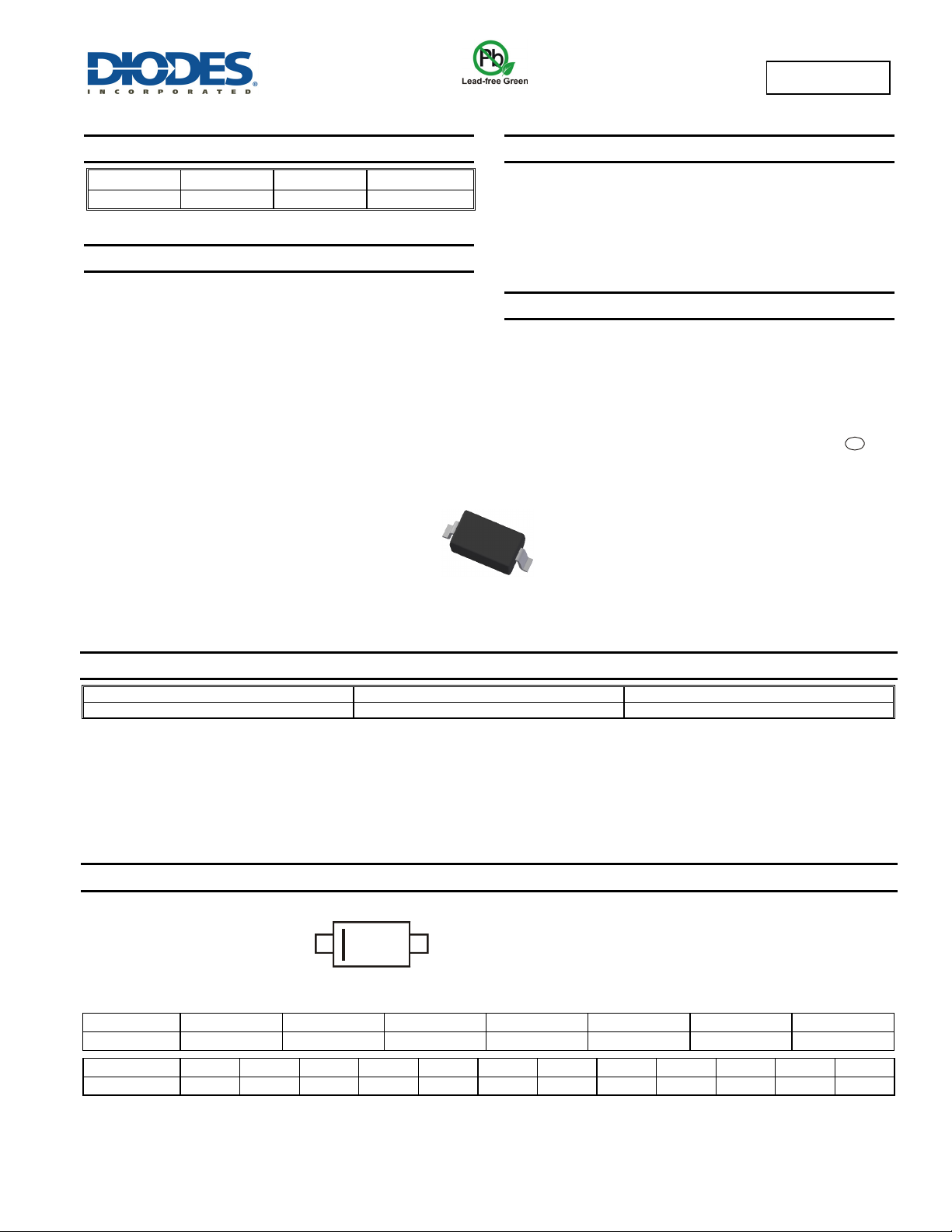
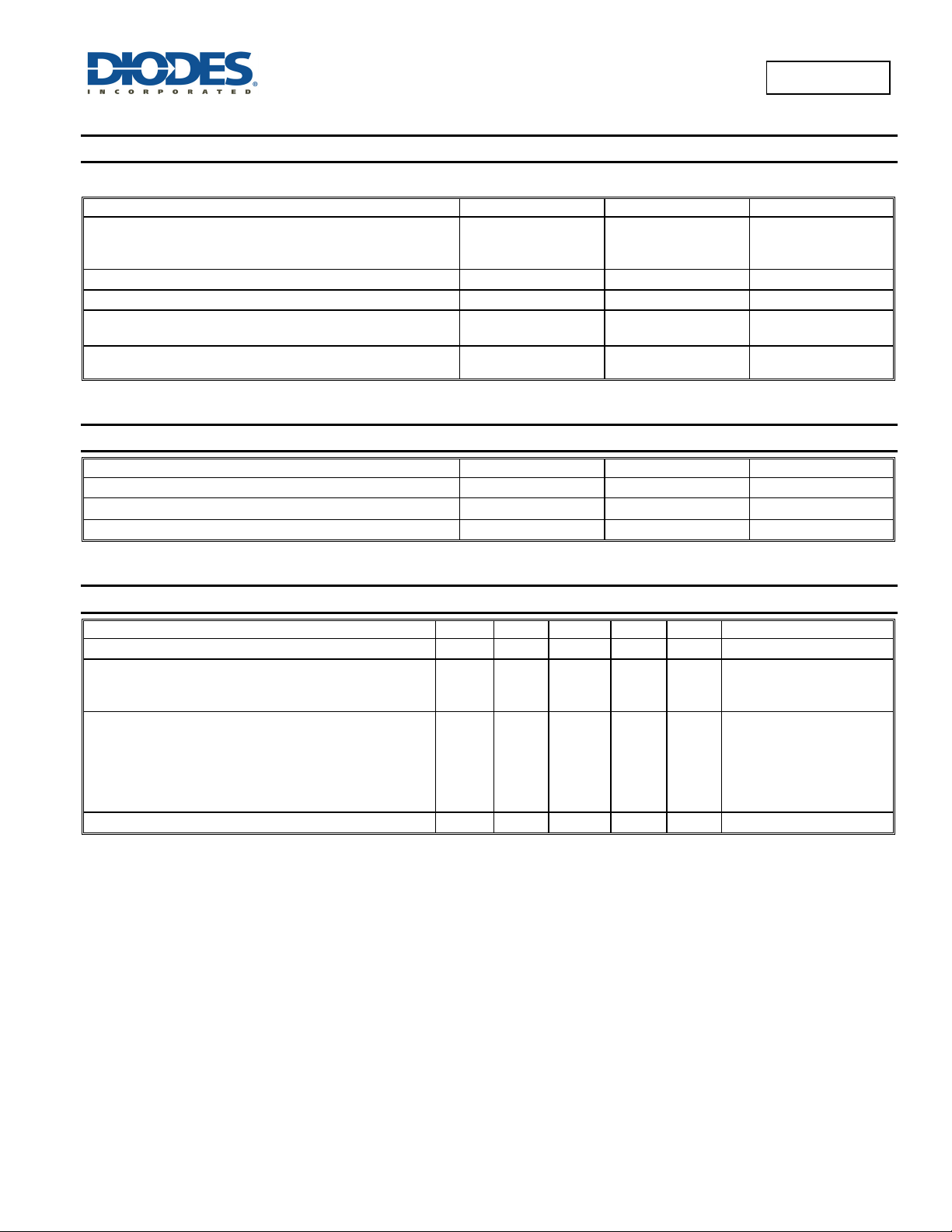
Diodes 1N5819HW Schematic [ru]

Product Summary (@ T
V
(V) IO (A) V
RRM
40 1.0 450 50
= +25°C)
A
F(MAX)
(mV) I
R(MAX)
Description and Applications
• For Use in Low Voltage, High Frequency Inverters
• Free Wheeling
• Polarity Protection Application
1N5819HW
1.0A SURFACE MOUNT SCHOTTKY BARRIER RECTIFIER
Features and Benefits
(µA)
• High Surge Capability
• Low Power Loss, High Efficiency
• High Current Capability and Low Forward Voltage Drop
• Guard Ring Die Construction for Transient Protection
• Totally Lead-Free & Fully RoHS Compliant (Notes 1 & 2)
• Halogen and Antimony Free. “Green” Device (Notes 3)
Mechanical Data
• Case: SOD123
• Plastic Material: Molded Plastic. UL Flammability Classification
Rating 94V-0
• Moisture Sensitivity: Level 1 per J-STD-020
• Polarity: Cathode Band
• Leads: Matte Tin Finish annealed over Alloy 42 leadframe (Lead
Free Plating) Solderable per MIL-STD-202, Method 208
• Weight: 0.01 grams (approximate)
Top View
e3
Ordering Information (Note 4)
Part Number Case Packaging
1N5819HW-7-F SOD-123 3000/Tape & Reel
Notes: 1. No purposely added lead. Fully EU Directive 2002/95/EC (RoHS) & 2011/65/EU (RoHS 2) compliant
and Lead-free.
<1000ppm antimony compounds.
.
2.. See http://www.diodes.com/quality/lead_free.htmlfor more information about Diodes Incorporated’s definitions of Halogen- and Antimony-free, "Green"
3. Halogen and Antimony free "Green” products are defined as those which contain <900ppm bromine, <900ppm chlorine (<1500ppm total Br + Cl) and
4. For packaging details, go to our website at http://www.diodes.com/datasheets/ap02007.pdf.
Marking Information
Date Code Key
Year 2011 2012 2013 2014 2015 2016 2017
Code Y Z A B C D E
Month Jan Feb Mar Apr May Jun Jul Aug Sep Oct Nov Dec
Code 1 2 3 4 5 6 7 8 9 O N D
SL
YM
1N5819HW
Document number: DS30217 Rev. 16 - 2
SL = Product Type Marking Code
YM = Date Code Marking
Y = Year (ex: B = 2014)
M = Month (ex: 9 = September)
1 of 5
www.diodes.com
June 2014
© Diodes Incorporated

1N5819HW
Maximum Ratings (@T
= +25°C, unless otherwise specified.)
A
Single phase, half wave, 60Hz, resistive or inductive load.
For capacitance load, derate current by 20%.
Characteristic Symbol Value Unit
Peak Repetitive Reverse Voltage
Working Peak Reverse Voltage @ I
= 1.0mA
R
DC Blocking Voltage
RMS Reverse Voltage
Average Rectified Output Current @ TL = +90°CI
Repetitive Peak Forward Current
t
1ms, δ ≤ 0.5
p
≤
Non-Repetitive Peak Forward Surge Current 8.3ms
Single Half Sine-Wave Superimposed on Rated Load
V
V
V
R(RMS)
I
FRM
I
FSM
RRM
RWM
V
R
O
40 V
28 V
1.0 A
1.5 A
25 A
Thermal Characteristics
Characteristic Symbol Value Unit
Power Dissipation (Note 5)
Typical Thermal Resistance Junction to Ambient (Note 5)
Operating and Storage Temperature Range
P
R
T
J, TSTG
D
JA
θ
Electrical Characteristics (@T
= +25°C, unless otherwise specified.)
A
Characteristic Symbol Min Typ Max Unit Test Condition
Reverse Breakdown Voltage (Note 3)
Forward Voltage
Reverse Leakage Current (Note 6)
Total Capacitance
Notes: 5. Device mounted on FR-4 PC Board, 2"x2", 2 oz. Copper, single sided, Cathode pad dimensions 0.75"x1.0", Anode pad dimensions 0.25"x1.0".
6. Short duration pulse test used to minimize self-heating effect.
V
(BR)R
V
F
I
R
C
T
40
⎯
⎯
⎯
⎯
⎯
⎯
⎯
⎯
⎯
⎯
⎯ ⎯
⎯
⎯
⎯
⎯
⎯
10
1
15
1.5
50 60 pF
450 mW
-65 to +125
0.320
0.450
0.750
1.0
10
50
2
75
3
222
V
V
mA
mA
µA
mA
µA
mA
IR = 1.0mA
= 0.1A
I
F
I
= 1.0A
F
= 3.0A
I
F
= 40V, TA = +25°C
V
R
= 40V, TA = +100°C
V
R
V
= 4V, TA = +25°C
R
V
= 4V, TA = +100°C
R
V
= 6V, TA = +25°C
R
V
= 6V, TA = +100°C
R
°C/W
°C
VR = 4V, f = 1.0MHz
1N5819HW
Document number: DS30217 Rev. 16 - 2
2 of 5
www.diodes.com
June 2014
© Diodes Incorporated
 Loading...