

Page 1
W
Please click here to visit our online spice models database.
Features
• Low Forward Voltage Drop
• Guard Ring Construction for Transient Protection
• Fast Switching Time
• Low Reverse Capacitance
• Surface Mount Package Ideally Suited for Automated Insertion
• Lead, Halogen and Antimony Free, RoHS Compliant
"Green" Device (Notes 3 and 4)
Maximum Ratings @T
Characteristic Symbol Value Unit
Peak Repetitive Reverse Voltage
Working Peak Reverse Voltage
DC Blocking Voltage
RMS Reverse Voltage
Maximum Forward Current
= 25°C unless otherwise specified
A
SURFACE MOUNT SCHOTTKY BARRIER DIODE
Mechanical Data
• Case: SOD-123
• Case Material: Molded Plastic. UL Flammability Classification
Rating 94V-0
• Moisture Sensitivity: Level 1 per J-STD-020D
• Terminals: Solderable per MIL-STD-202, Method 208
• Lead Free Plating (Matte Tin Finish annealed over Alloy 42
leadframe)
• Polarity: Cathode Band
• Marking Information: See Page 2
• Ordering Information: See Page 2
• Weight: 0.01 grams (approximate)
Top View
V
V
V
R(RMS)
RRM
RWM
VR
IFM
70 V
49 V
15 mA
1N5711
Thermal Characteristics
Characteristic Symbol Value Unit
Power Dissipation (Note 1)
Thermal Resistance, Junction to Ambient Air (Note 1)
Operating Temperature Range
Storage Temperature Range
Electrical Characteristics @T
Characteristic Symbol Min Typ Max Unit Test Condition
Reverse Breakdown Voltage (Note 2)
Forward Voltage Drop
Reverse Leakage Current (Note 2)
Total Capacitance
Reverse Recovery Time
Notes: 1. Part mounted on FR-4 board with recommended pad layout, which can be found on our website at http://www.diodes.com/datasheets/ap02001.pdf.
2. Short duration pulse test used to minimize self-heating effect.
3. No purposefully added lead. Halogen and Antimony Free.
V9 are built with Non-Green Molding Compound and may contain Halogens or Sb
1N5711W
Document number: DS11015 Rev. 14 - 2
4. Product manufactured with Data Code V9 (week 33, 2008) and newer are built with Green Molding Compound. Product manufactured prior to Date Code
= 25°C unless otherwise specified
A
PD
R
JA
θ
TJ
T
STG
70
1 of 3
V
(BR)R
VF ⎯ ⎯
IR ⎯ ⎯
CT ⎯ ⎯
trr ⎯ ⎯
www.diodes.com
-55 to +125
-55 to +150
⎯ ⎯
0.41
1.00
200 nA
2.0 pF
1.0 ns
Fire Retardants.
2O3
333 mW
300
V
IR = 10μA
IF = 1.0mA
V
IF = 15mA
VR = 50V
VR = 0V, f = 1.0MHz
IF = IR= 5.0mA
I
= 0.1 x IR, RL = 100Ω
rr
°C/W
°C
°C
July 2008
© Diodes Incorporated
Page 2
W
TANT
O
U
O
RWAR
CUR
RENT
TANT
O
US R
R
C
URRENT
C, TOT
CAPACITAN
C
F
P, P
OWER
PATIO
N
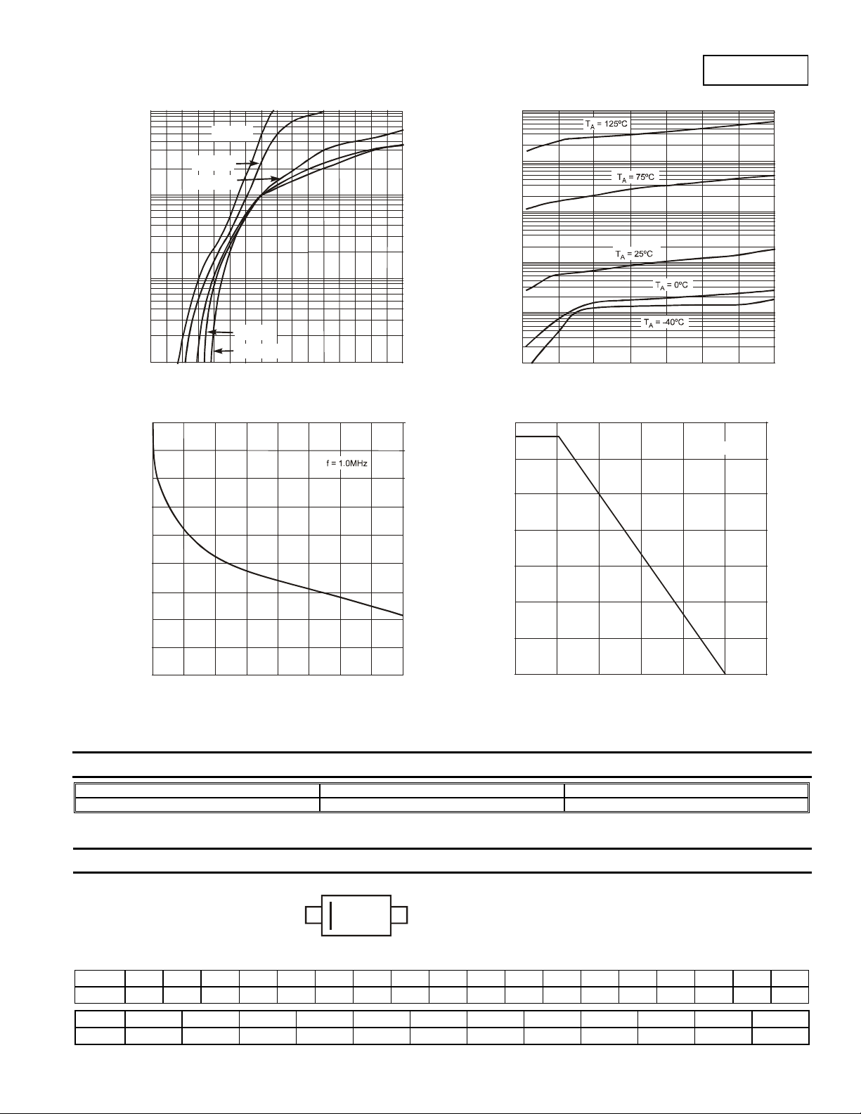
1N5711
10,000
(nA)
1,000
SE
100
(mA)
D
100
10
T = 125ºC
A
T = 75ºC
A
T = 25ºC
A
EVE
S F
10
1.0
ANE
T = 0ºC
A
T = -40ºC
0.1
F
I , INS
0
V , INSTANTANEOUS FORWARD VOLTAGE (V)
F
0.4
A
0.8
1.0
0.60.2
Fig. 1 Typical Forward Characteristics
1.8
1.6
)
1.4
E (p
1.2
1.2
1.4
1.6
ANE
R
I , INS
(mW)
1
0.1
0
V , INSTANTANEOUS REVERSE VOLTAGE (V)
R
2010 30 605040
Fig. 2 Typical Reverse Characteristics
350
300
250
70
Note 1
1.0
0.8
AL
0.6
T
0.4
0.2
0
0
105
V , DC REVERSE VOLT AGE (V)
R
15
20 25
Fig. 3 Total Capacitance vs. Reverse Voltage
30
35
40
200
150
DISSI
100
D
50
0
025
75
100
50
T , AMBIENT TEMPERATURE (°C)
A
125 150
Fig. 4 Power Derating Curve
Ordering Information (Note 5)
Part Number Case Packaging
1N5711W-7-F SOD-123 3000/Tape and Reel
Notes: 5. For packaging details, go to our website at http://www.diodes.com/datasheets/ap02007.pdf.
Marking Information
SA
YM
Date Code Key
Year 1998 1999 2000 2001 2002 2003 2004 2005 2006 2007 2008 2009 2010 2011 2012 2013 2014 2015
Code J K L M N P R S T U V W X Y Z A B C
Month Jan Feb Mar Apr May Jun Jul Aug Sep Oct Nov Dec
Code 1 2 3 4 5 6 7 8 9 O N D
1N5711W
Document number: DS11015 Rev. 14 - 2
SA = Product Type Marking Code
YM = Date Code Marking
Y = Year (ex: T = 2006)
M = Month (ex: 9 = September)
2 of 3
www.diodes.com
July 2008
© Diodes Incorporated
Page 3

W
1N5711
Package Outline Dimensions
B
M
C
H
SOD-123
A
K
L
Dim Min Max
A 0.55 Typ
B 1.40 1.70
C 3.55 3.85
H 2.55 2.85
J 0.00 0.10
K 1.00 1.35
L 0.25 0.40
M 0.10 0.15
α
All Dimensions in mm
0 8°
Suggested Pad Layout
Diodes Incorporated and its subsidiaries reserve the right to make modifications, enhancements, improvements, corrections or other changes
without further notice to any product herein. Diodes Incorporated does not assume any liability arising out of the application or use of any product
described herein; neither does it convey any license under its patent rights, nor the rights of others. The user of products in such applications shall
assume all risks of such use and will agree to hold Diodes Incorporated and all the companies whose products are represented on our website,
harmless against all damages.
Diodes Incorporated products are not authorized for use as critical components in life support devices or systems without the expressed written
approval of the President of Diodes Incorporated.
X
Y
C
Dimensions Value (in mm)
Z 4.9
G 2.5
X 0.7
Y 1.2
C 3.7
G
Z
IMPORTANT NOTICE
LIFE SUPPORT
1N5711W
Document number: DS11015 Rev. 14 - 2
3 of 3
www.diodes.com
July 2008
© Diodes Incorporated
 Loading...