

Page 1

PC, DVI INTERFACE CONTROLLER
FOR TFT PANEL
Model: HE-1400v2
Part number : 41758012X-3 or up
INSTRUCTIONS
CONTENTS
Page: 2. Introduction, How to Proceed, Usage Note, Disclaimer
3. System design – Diagram of a suggested system
4. Assembly notes – Important information about system elements
6. Connection & Operation – How to use the controller
10. Connectors, pinouts & jumpers – Essential connection information
18. Controller dimensions
19. Application notes
21. Troubleshooting
22. Specifications
23. Appendix I – Graphic Mode Support Table
25. Appendix II – RS-232 control protocols
30. Appendix III – Mapping definition
32. Appendix IV – Color Auto Adjust
33. Warranty, Caution & Limitation of Liability, Trademarks
34. Contact details
35. Revision history
It is essential that these instructions are read and understood before connecting or
powering up this controller.
Specifications subject to change without notice
© Digital View Ltd – Doc Ver 2.00: 15 November, 2017 Page
1 of 35
Page 2
Introduction
HE-1400v2 is the harsh Environment version of the ALR-1400v2. Provides full ALR-1400v2 feature set, plus wide range
operating temperature and voltage range; shock and vibration tolerance and conformal coating for extreme
environment applications.
TFT (active matrix) LCDs with LVDS interface of 1440x900, 1366x768, 1280x1024, 1280x800, 1024x768, 800x600,
640x480 resolution;
Computer video signals of SXGA, XGA, SVGA, VGA standard
Support LVDS or TTL interface panel
Low mass tantalum capacitors for maximum vibration and shock tolerance, conformal coating, operating
temperature range from -20oC to +80oC plus calculated MTBF in excess of 100K hours.
Overall suitability for usage in critical applications must be independently tested and verified by the user.
Ordering information :
Controller Part number Ordering part number
HE-1400v2 P/N 41758012X-3 P/N 4175801XX-3
HOW TO PROCEED
Ensure you have all parts & that they are correct, refer to:
• Connection diagram (separate document for each panel)
• Connector reference (in following section)
• Assembly notes
Check controller switch & jumper settings (errors may damage the panel)
Prepare the PC
Connect the parts
Understand the operation and functions (in following section)
IMPORTANT USAGE NOTE
This product is for use by system developers and integrators, the manufacturer accepts no liability for damage or
injury caused by the use of this product. It is the responsibility of the developer, integrators or other user of this
product to:
Ensure that all necessary and appropriate safety measures are taken.
Obtain suitable regulatory approvals as may be required.
Check power settings to all component parts before connection.
Understand the operation and connectivity requirements of this controller.
DISCLAIMER
There is no implied or expressed warranty regarding this material.
Specifications subject to change without notice
© Digital View Ltd – Doc Ver 2.00: 15 November, 2017 Page
2 of 35
Page 3
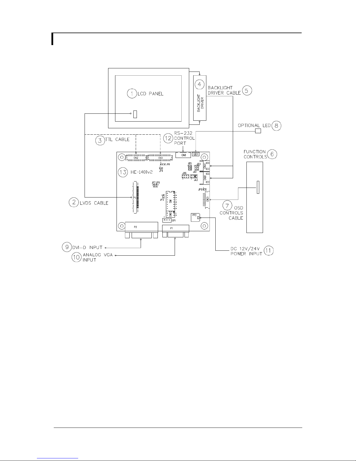
SYSTEM DESIGN
A typical LCD based display system utilising this controller is likely to comprise the following:
Summary:
1. LCD panel
2. LVDS cable (for connection with LVDS panel)
3. TTL cable (for connection with TTL panel)
4. Backlight driver (if not built into LCD)
5. Backlight driver cable
6. Function controls
7. Function controls cable
8. Status LED
9. DVI-D input
10. Analog VGA input
11. Power input (12VDC / 24VDC)
12. RS-232 control port
13. LCD controller card, HE-1400v2
Digital View offers a range of accessories such as listed above, to make up complete display solution.
Specifications subject to change without notice
© Digital View Ltd – Doc Ver 2.00: 15 November, 2017 Page
3 of 35
Page 4

ASSEMBLY NOTES
This controller is designed for monitor and custom display projects using 1440x900, 1366x768, 1280x1024, 1280x800,
1024x768, 800x600, 640x480 resolution TFT panels with a SXGA, WXGA, XGA, SVGA, VGA signal input. The following
provides some guidelines for installation and preparation of a finished display solution.
Preparation: Before proceeding it is important to familiarize yourself with the parts making up the system and the various
connectors, mounting holes and general layout of the controller. As much as possible connectors have been labeled. Guides
to connectors and mounting holes are shown in the following relevant sections.
1. LCD Panel: This controller is designed for typical LVDS or TTL interface TFT panels with panel voltage 3.3V or 5V or 12V
or 18V LVDS interface. Due to the variation between manufacturers of signal timing and other panel characteristics
factory setup and confirmation should be obtained before connecting to a panel. (NOTE: Check panel power jumper
settings before connection)
2. Controller card: Handle the controller card with care as static charge may damage electronic components.
3. LVDS signal cable : In order to provide a clean signal it is recommended that LVDS signal cables are no longer than
46cm (18 inches). If loose wire cabling is utilized these can be made into a harness with cable ties. Care should be
taken when placing the cables to avoid signal interference. Additionally it may be necessary in some systems to add
ferrite cores to the cables to minimize signal noise.
4. TTL signal cable: In order to provide a clean signal it is recommended that LCD signal cables are no longer than 33cm
(13 inches). If loose wire cabling is utilized these can be made into a harness with cable ties. Care should be taken when
placing the cables to avoid signal interference. Additionally it may be necessary in some systems to add ferrite cores to
the cables to minimize signal noise.
5. Backlight driver: This will be required for the backlight of an LCD, some LCD panels have an built in backlight driver. As
panels may have 1 or more backlight tubes and the power requirements for different panel models backlights may vary it
is important to match the backlight driver in order to obtain optimum performance. See page 20 for the Application notes
“Backlight driver connection section for more informations.
6. Backlight driver Cables: Different backlight driver models require different cables and different pin assignment. Make
sure correct cable pin out to match the backlight driver. Using wrong cable pin out may damage the backlight driver.
7. Function Controls: The following section discusses the controls required and the section on connectors provides the
detail. The controls are minimal: On/Off, Backlight Brightness (depends on backlight driver), OSD (5 momentary buttons)
analog VR type or (8 momentary buttons) digital type.
8. Function controls cable: The cables to the function switches should be of suitable quality and length so that impedance
does not affect performance. Generally lengths up to 1 metre (3 feet) should be acceptable.
9. DVI-D Input Cable : Plug the DVI-D cable to the connector P2 on the controller board
10. Analog VGA Input Cable: As this may affect regulatory emission test results and the quality of the signal to the
•••• Power Input: 12V / 24V DC is required, this should be a regulated supply. Although the controller provides power
24VDC input is required when the panel output voltage is 18VDC. Please refer to page 12-13 for proper jumper settings.
•••• Power Safety: Note that although only 12VDC / 24VDC is supplied as ‘power-in’ a backlight driver for panel backlighting
•••• EMI: Shielding will be required for passing certain regulatory emissions tests. Also the choice of external Controller to PC
•••• Ground: The various PCB mounting holes are connected to the ground plane.
•••• Servicing: The board is not user serviceable or repairable. Warranty does not cover user error in connecting up to the
•••• Controller Mounting: It is recommended that a clearance of at least 10mm is provided above and 5mm below the
Specifications subject to change without notice
© Digital View Ltd – Doc Ver 2.00: 15 November, 2017 Page
controller, a suitably shielded cable should be utilized.
regulation for the LCD power this does not relate to the power supplied to the backlight driver. If an unregulated power
supply is provided to an backlight driver any fluctuations in power may affect operation, performance and lifetime of the
backlight driver and or backlight tubes.
produces significantly higher voltages (the backlight driver does not connect to the ground plane). We strongly advise
appropriate insulation for all circuitry.
signal cable can affect the result.
controller and is invalidated by unauthorized modification or repairs.
controller when mounted. Additionally consideration should be given to:
• Electrical insulation.
• Grounding.
• EMI shielding.
• Cable management. Note: It is important to keep panel signal cables apart from the backlight drivers & backlight
cables to prevent signal interference.
• Heat & Ventilation: Heat generated from other sources, for example the backlight of a very high brightness panel
may generate significant heat which could adversely affect the controller.
4 of 35
Page 5

• Other issues that may affect safety or performance.
•••• PC Graphics Output: A few guidelines:
• Signal quality is very important, if there is noise or instability in the PC graphics output this may result in visible noise
on the display.
• Refer to graphics modes table in specifications section for supported modes.
• Non-interlaced & interlaced video input is acceptable.
IMPORTANT: Please read the Application Notes section for more information.
Specifications subject to change without notice
© Digital View Ltd – Doc Ver 2.00: 15 November, 2017 Page
5 of 35
Page 6
CONNECTION & OPERATION
CAUTION: Never connect or disconnect parts of the display system when the system is powered up as this may cause serious
damage.
CONNECTION
Connection and usage is quite straight forward (it is useful to have the relevant connection diagram available at this time):
1. LCD panel & Backlight driver: Connect the backlight driver (if it is not built-in the panel) to the CCFT lead
2. LVDS type panels: Plug the LVDS signal cable direct to J1 (if necessary). Insert the panel end of the cable to the
LCD panel connector.
3. TTL type panels: Plug the signal cables direct to CN2 or CN3. Plug the other end of cables to the LCD connector
board (if connector board is required, otherwise the signal can be direct plug to the LCD panel
connector). Then plug the board connector to the LCD panel connector.
4. Backlight driver & Controller: Plug the backlight driver cable to CNB1 and CNA1 (if necessary). Plug another end
5. Function switch & Controller: Plug the OSD switch mount cable to CNC1 on the controller board and another to
the OSD switch mount.
6. LED & Controller: Plug in a 3-way with dual color LED to connector LED1 on the controller board.
7. Jumpers : Check all jumpers are set correctly. Details referring the connection diagram at
http://www.digitalview.com/controllers/csg.php
8. Jumpers & Backlight driver & Panel voltage: Particularly pay attention to the settings of JA3, JA6, JB2, JB3. JB2
9. DVI cable : Plug the DVI-D cable to the connector P2 on the controller board.
10. VGA cable & Controller: Plug the VGA cable to the connector P1 on the controller board.
12. Power supply & Controller: Plug the DC 12V / 24V power in to the connector PP2. You can consider to use
13. Power on: Switch on the controller board and panel by using the OSD switch mount.
CAUTION: Never connect or disconnect parts of the display system when the system is powered up as this may cause serious
damage.
LED status :
General:
• If you are using supplied cables & accessories, ensure they are correct for the model of panel and controller.
• If you are making your own cables & connectors refer carefully to both the panel & backlight driver specifications and the
PC SETTINGS
The controller has been designed to take a very wide range of input signals however to optimize the PC’s graphics
performance we recommend choosing 60Hz vertical refresh rate – this will not cause screen flicker.
OPERATION
Once the system has been connected and switched on there are a number of functions available to adjust the display
image as summarized in the following sections. The settings chosen will be saved for each mode independently.
connector of the LCD panel.
to the connector on the backlight driver.
& JB3 are used for backlight driver control (read backlight driver specification and information on the jumper table to
define the correct settings). JA3 & JA6 are used for panel voltage input (read panel specification and information on
the jumper table to define the correct settings).
DigitalView mating power cable P/N 426013800-3, 160mm.
State LED color
No signal & backlight off RED
With signal & backlight on GREEN
section in this manual, “Connectors, Pinouts & Jumpers” to ensure the correct pin to pin wiring.
Specifications subject to change without notice
© Digital View Ltd – Doc Ver 2.00: 15 November, 2017 Page
6 of 35
Page 7
LCD DISPLAY SYSTEM SETTINGS
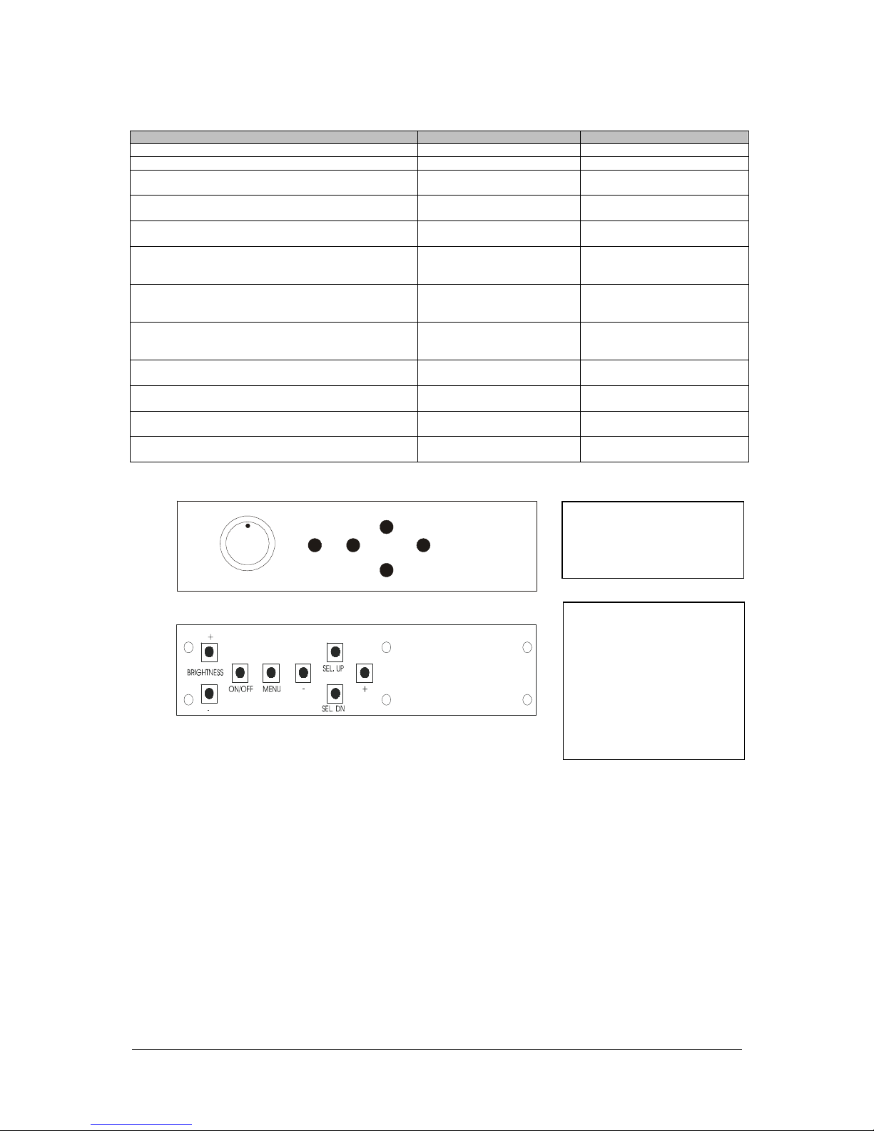
NOTE: By way of explanation the following refers to a set of sample buttons that may be obtained as an option. In
addition to power on/off and connection for backlight brightness the controller provides an On Screen Display of certain
functions which are controlled by 5 momentary type buttons (analog VR type) or 8 momentary type buttons (digital type):
Controls Analog VR type Digital type
On/Off – turns controller board power on VR toggle switch On/Off button
Brightness – controls backlight brightness Rotary VR Brightness +/- buttons
Menu – turns OSD menu On or Off (it will auto time
off)
Select – Select function / Confirm
(under OSD menu on state)
Move up / down to select OSD menu function
(under OSD menu on state)
+ – increase the setting / moves the selector to the
next function
(under OSD menu on state)
- - decrease the setting / moves the selector to the
previous function
(under OSD menu on state)
Reset to Factory Defaults Press and hold SEL DN
Direct access key for Brightness level increase
(under OSD menu off state)
Direct access key for Brightness level decrease
(under OSD menu off state)
Direct access key for Backlight Brightness increase*
(under OSD menu off state)
Direct access key for Backlight Brightness decrease*
(under OSD menu off state)
* No OSD menu display when adjusting the "Backlight" hotkey function
Menu button Menu button
SEL DN SEL DN
SEL UP SEL UP
+ +
- -
button, then power on the
controller
+ +
- -
SEL UP SEL UP
SEL DN SEL DN
SEL UP
Press and hold SEL DN button,
then power on the controller
12V / 24VDC power input :
Analog 10K VR Type OSD
ON/Off/Brightness
Menu
-
+
SEL DN
switch mount uses
P/N 410680550-3 or up
Analog VR type
12V / 24VDC power input :
Digital 10K Type OSD
switch mount uses
P/N 416100520-3 or up
12VDC power input :
Digital 10K Type OSD
Digital type
switch mount uses
P/N 416100510-3
Specifications subject to change without notice
© Digital View Ltd – Doc Ver 2.00: 15 November, 2017 Page
7 of 35
Page 8
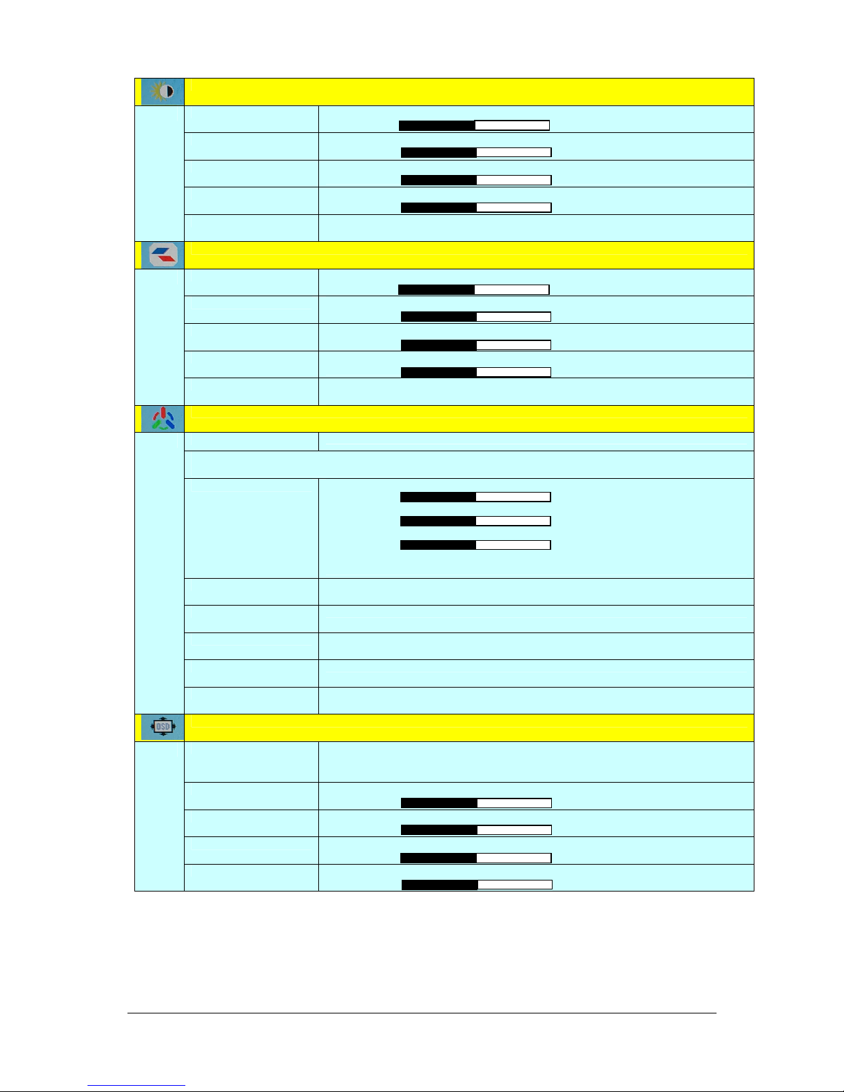
OSD Functions
Picture
Brightness
Contrast
Sharpness
Backlight
Invert
Display
H. Position*
V. Position*
Clock*
Phase*
Aspect
Color
Gamma
Color Temperature 4444 (Adjust the warmness of the image displayed. The higher temperature the
coolest image looks like. The lower temperature the warmest image looks like.)
User
4200K
Increase/decrease brightness level.
Press – or + (- + ) Total : 100 steps
Increase/decrease panel contrast level.
Press – or + (- + ) Total : 100 steps
Increase/decrease shapness level.
Press – or + (- + ) Total : 7 steps
Increase/decrease backlight brightness level.
Press – or + (- + ) Total : 100 steps
B/L Invert : Invert for the backlight brightness
Use +/- to move the image horizontally.
Press – or + (- + ) Total : 100 steps
Use +/- to move the image vertically.
Press – or + (- + ) Total : 100 steps
Adjust the image horizontal size.
Press – or + (- + ) Total : 100 steps
Fine tune the data sampling position (adjust image quality)
Press – or + (- + ) Total : 100 steps
WIDE : Scaling format to Fill screen
4:3 : Scaling format in 4:3
1.8 / 2.0 / 2.2 / 2.4 / 2.6 : Adjust Gamma settings
Adjust red color level
Press – or + (- +) Total :100 steps
Adjust green color level
Press – or + (- +) Total : 100 steps
Adjust blue color level
Press – or + (- +) Total : 100 steps
Press SEL UP/DN button to select item
Set the color temperature to 4200K
5000K
6500K
7500K
9300K
OSD Setting
Specifications subject to change without notice
© Digital View Ltd – Doc Ver 2.00: 15 November, 2017 Page
Language
OSD H. POS.
OSD V. POS.
OSD TIMER
Transparency
Set the color temperature to 5000K
Set the color temperature to 6500K
Set the color temperature to 7500K
Set the color temperature to 9300K
Press SEL UP/DN button to select item
English / French / Spanish
Adjust OSD menu Horizontal position.
Press – or + (- + ) Total : 100 steps
Adjust OSD menu Vertical position.
Press – or + (- + ) Total : 100 steps
OSD Timeout : 0 / 10 / 20 / 30 / 40 / 50 / 60 seconds (Always on when set to 0)
Press – or + (- + )
Set the OSD menu transparency level : 0 / 25 / 50 / 75 / 100
Press – or + (- + ) Total : 5 steps
8 of 35
Page 9
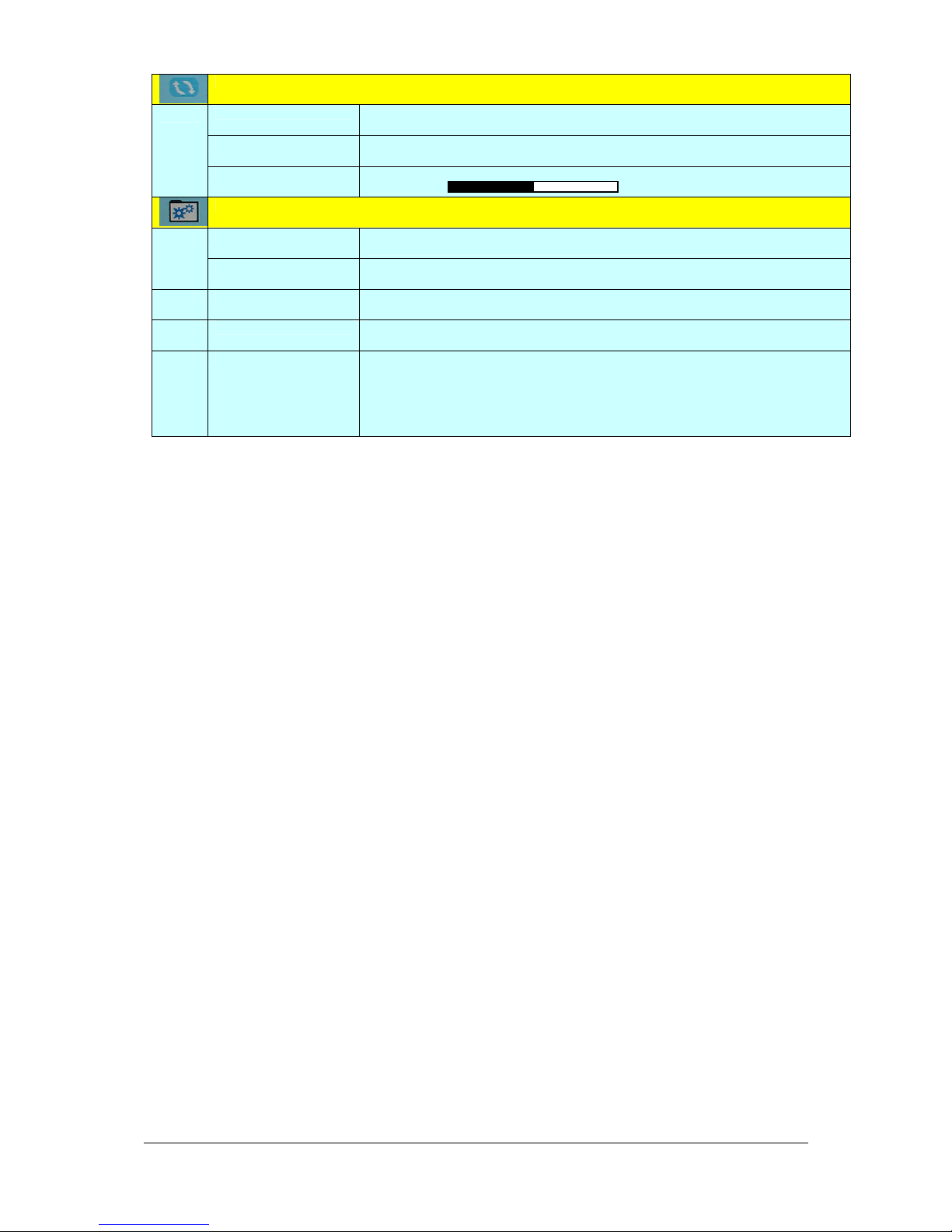
Reset
* Function in VGA mode only
Items marked 4 have sub menus.
Exit the OSD menu to save the setting chosen
Image Auto Adjust*
Color Auto Adjust*
Factory Reset
Others
Signal Source
Auto Source Seek
B/L Control
PWM FREQ
Wide screen mode*
Auto adjust the positions, phase, frequency
Auto color calibration [See Appendix IV]
OSD Timeout : 0 / 10 / 20 / 30 / 40 / 50 / 60 seconds (Always on when set to 0)
Press – or + (- + )
DVI : Select input source to DVI
VGA : Select input source to VGA
ON : Auto source select always enable
OFF : Disable auto source select function
DA or PWM : Selection for voltage level dimming control / PWM dimming control
Backlight frequency 100 ~ 440 in a step of 20
Select the input mode (1280 / 1360 / 1366 / 1368) to recognize and display the correct
input signal information display on the OSD menu.
1280x768
1360x768
1366x768
1368x768
Firmware V1.06.00 or up
Specifications subject to change without notice
© Digital View Ltd – Doc Ver 2.00: 15 November, 2017 Page
9 of 35
Page 10
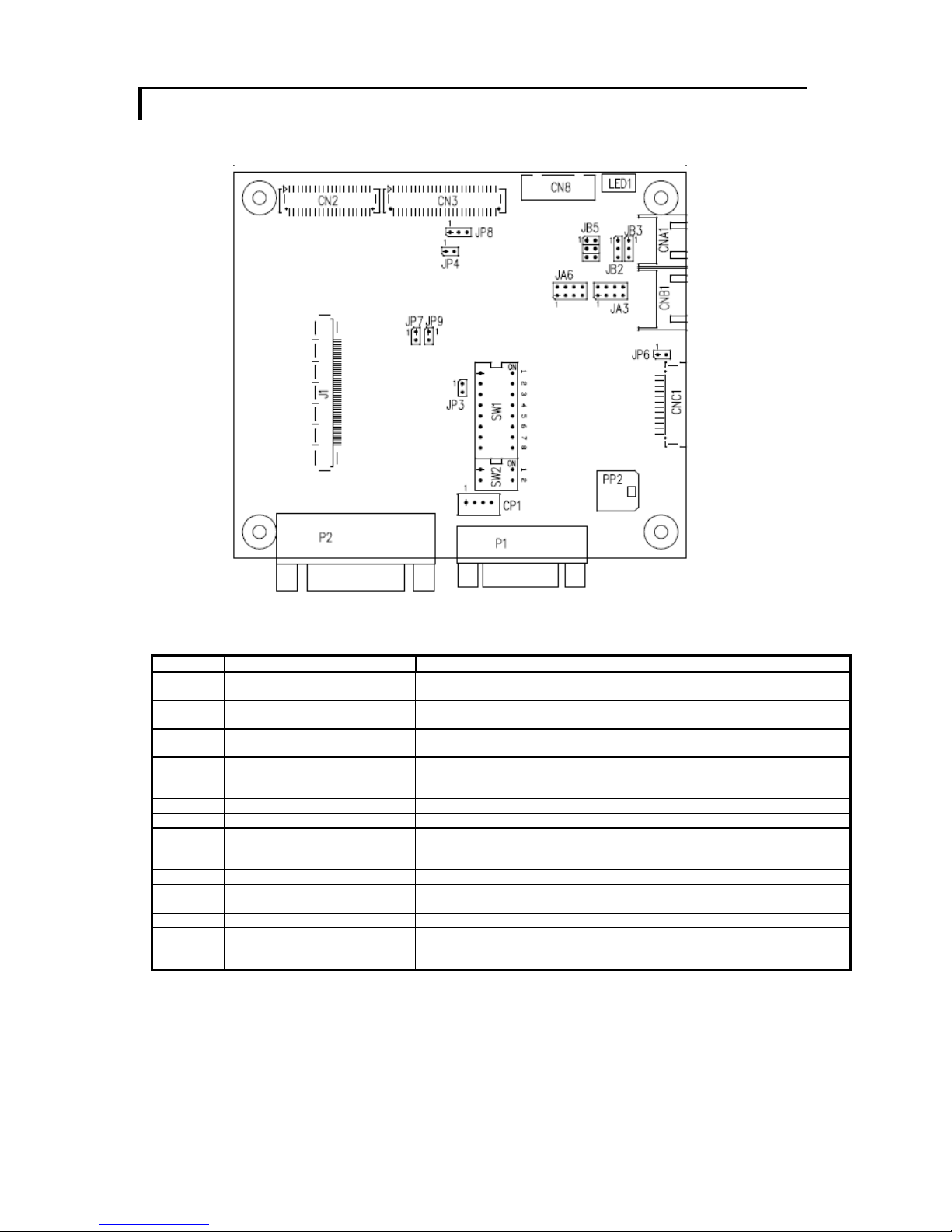
CONNECTORS, PINOUTS & JUMPERS
The various connectors are:
Summary: Connectors
Ref Purpose Description
J1 LVDS Panel Signal STARCONN : 115E51-0000RA-M3-R
CN2 TTL Panel Signal Hirose 40-pin, DF20G-40DP-1V
CN3 TTL Panel Signal Hirose 50-pin, DF20G-50DP-1V
CN8 Serial control (for firmware
programming or RS-232 control
use only)
CNA1 Auxiliary Power Output JST 4-way, S4B-XH-A compatible (Mating type : XHP-4 or compatible)
CNB1 Backlight control connector JST 5-way, S5B-XH-A compatible (Mating type : XHP-5 or compatible)
CNC1 OSD controls Hirose DF13A-12P-1.25H compatible (Mating type : DF13-12S-1.25C)
CP1 Internal programming connector JST PHD-4 compatible (Mating type : PHR-4 or compatible)
LED1 Dual color status LED connector JST 3-way, B3B-XH-A compatible (Mating type : XHP-3 or compatible)
P1 VGA input DB-15 way high density 3 row
P2 DVI-D input DVI-D connector
PP2 Main Input Power Molex 43650-0200 compatible (Mating type : Molex 43645-0200
(Matching type : STARCONN 107D51-000001-00 or compaible)
(Mating type : DF20A-40DS-1C)
(Mating type : DF20A-50DS-1C)
JST 6-way, B6B-XH-A compatible (Mating type : XHP-6 or compatible)
(Matching OSD switch mount cable P/N 426122200-3 (150mm) or 426122210-3
(250mm)
compatible)
(Matching power cable : P/N 426013800-3)
Specifications subject to change without notice
© Digital View Ltd – Doc Ver 2.00: 15 November, 2017 Page
10 of 35
Page 11
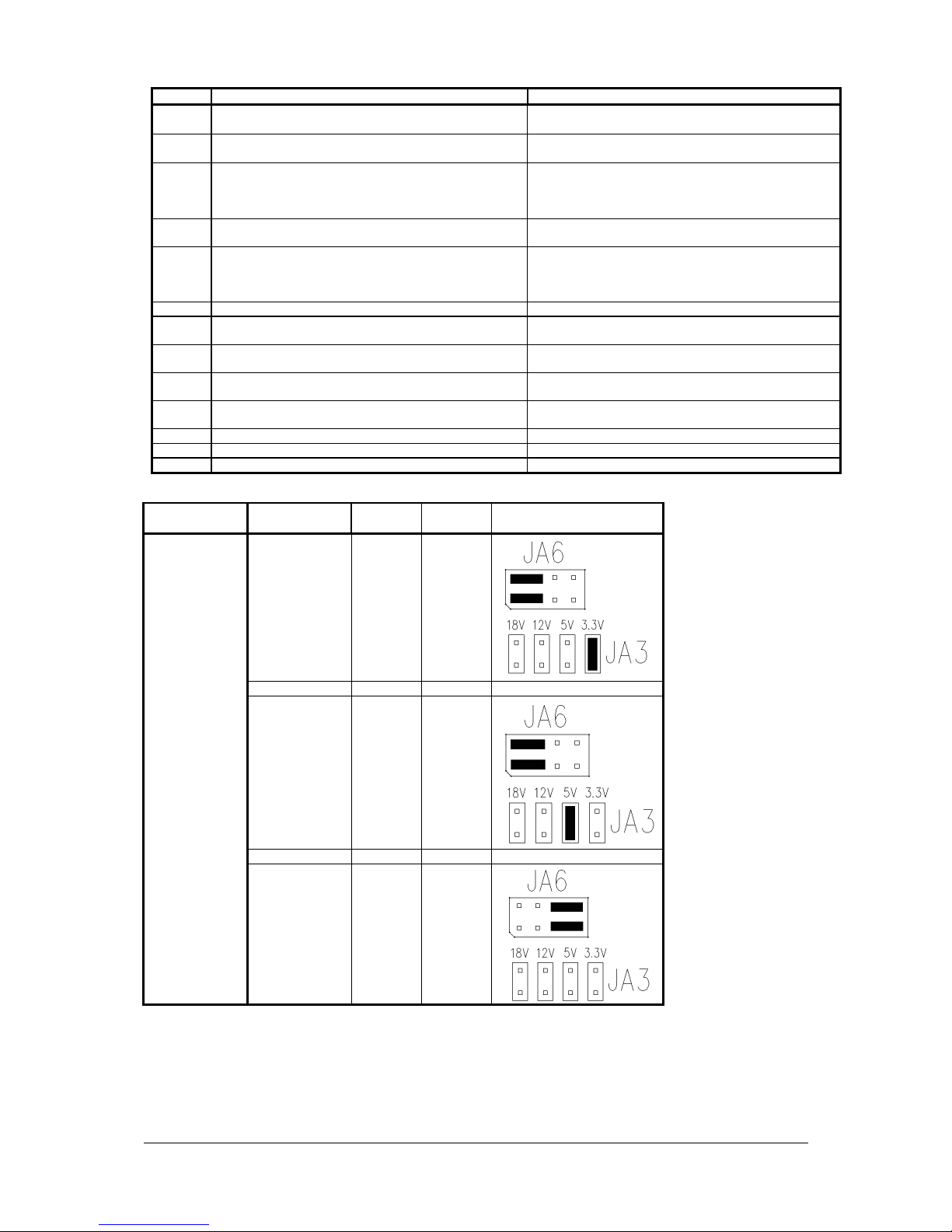
Summary: Jumpers setting
Ref Purpose Note
JA3 Panel power voltage select See panel voltage setting table 1
JA6 Panel power voltage select See panel voltage setting table 1
JB2 Backlight on/off control – signal level 1-2 = On/Off control signal ‘High’ = +3.3V
JB3 Backlight on/off control – polarity 1-2 = control signal ‘high’ = CCFT ON
JB5 Backlight control type selection 1-2 = VR/Digital switch mount control
JP3 Reserved Default Open
JP4 LVDS or TTL panel selection Close = LVDS panel
JP6 Input power control Short = External switch control
JP7 Reserved Reserved for internal programming use (Always 1-2
JP8 Clock phase (Analog RGB) 1-2 = Normal
JP9 Reserved 1-2 = Default
SW1 Panel selection See table below
SW2 Panel selection See table below
Table 1 : Panel voltage setting table :
Input voltage via
PP2 Panel Voltage JA3 JA6 Jumper on board
CAUTION: Incorrect setting will cause panel damage
CAUTION: Incorrect setting will cause panel damage
2-3 = On/Off control signal ‘High’ = +5V
Open = On/Off control signal ‘High’ = Open collector
CAUTION: Incorrect setting can damage backlight driver.
2-3 = control signal ‘low’ = CCFT ON
3-4 = Analog backlight brightness controlled by RS-232 –
voltage range 0~5V
5-6 = PWM (Pulse Width Modulation) brightness
Open = TTL panel
Open = Switch mount control
closed)
2-3 = Invert
3.3V 3V3 closed 1-3 & 2-4
12VDC
CAUTION: Incorrect setting can damage panel & controller
5V 5V closed 1-3 & 2-4
12V OPEN 5-7 & 6-8
Specifications subject to change without notice
© Digital View Ltd – Doc Ver 2.00: 15 November, 2017 Page
11 of 35
Page 12
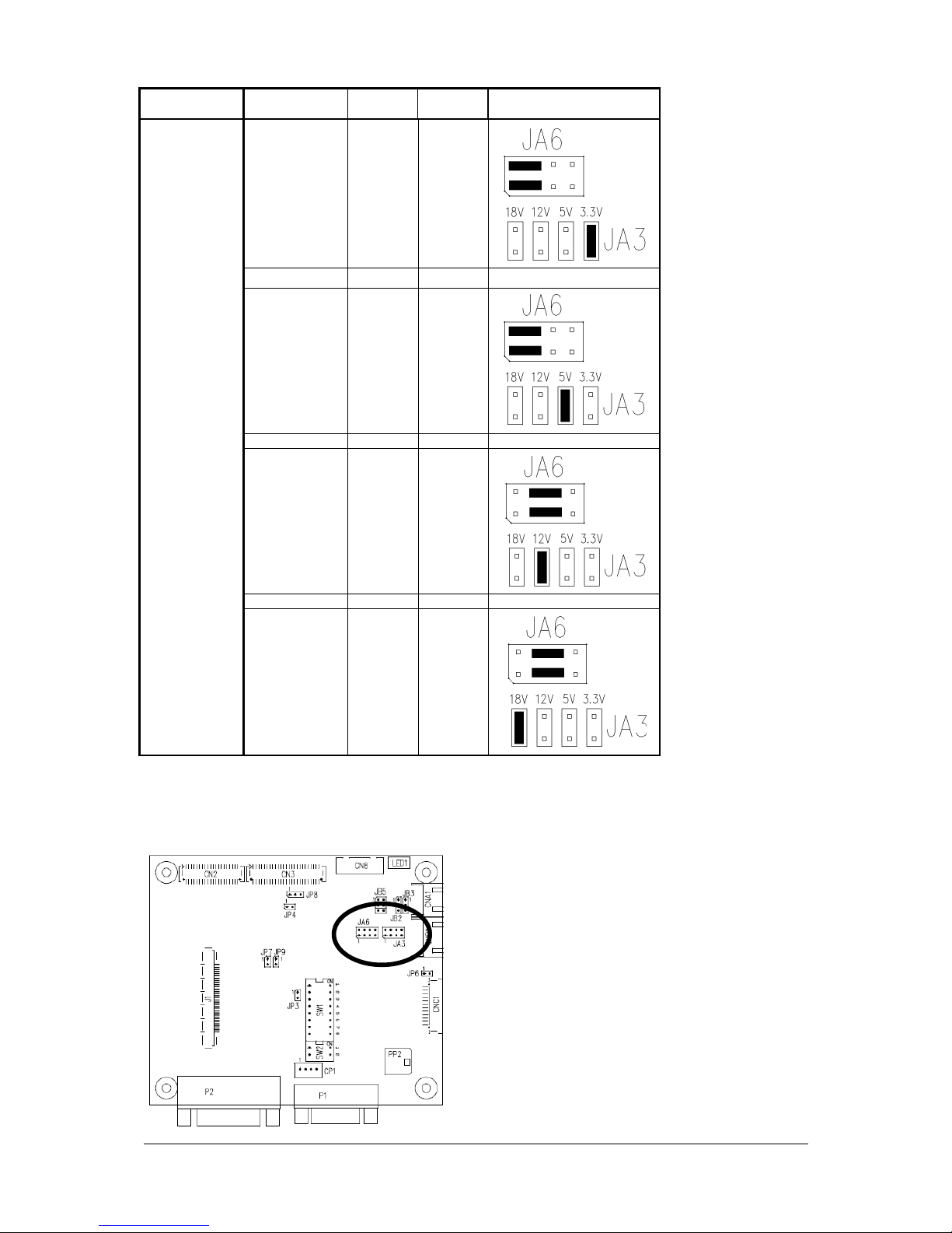
Input voltage via
PP2 Panel Voltage JA3 JA6 Jumper on board
3.3V 3V3 closed 1-3 & 2-4
24VDC**
5V 5V closed 1-3 & 2-4
12V 12V closed 3-5 & 4-6
18V 18V closed 3-5 & 4-6
** Please make sure the backlight power must support 24V supply. Because CNA1 pin 1 and
CNB1 pin 2 will output 24VDC if input 24VDC via PP2.
JA3 & JA6 location on board : (Please pay attention to the jumper settings on JA3 & JA6 which are
red in color on board)
!
Specifications subject to change without notice
© Digital View Ltd – Doc Ver 2.00: 15 November, 2017 Page
12 of 35
Page 13
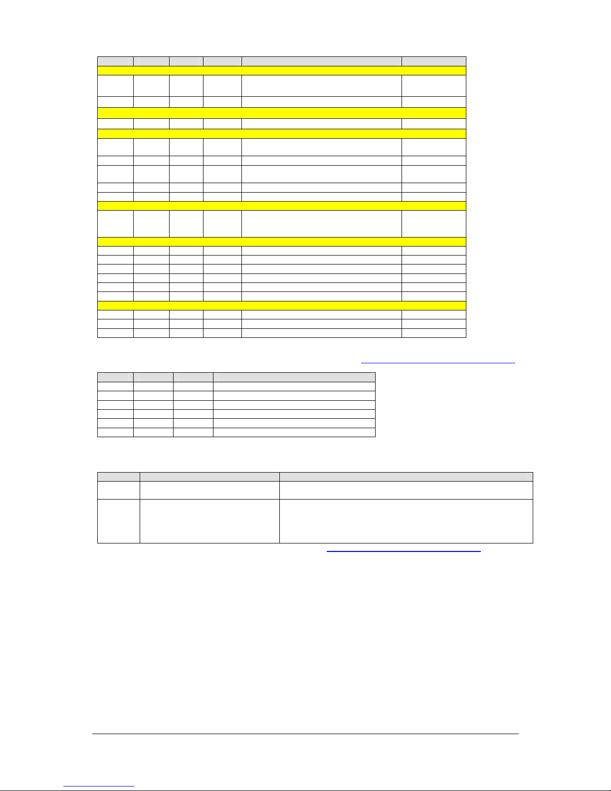
DIP Switch selection – SW1
(1)
(1)
(1)
(1)
Pos #1 Pos #2 Pos #3 Pos.#4 Description Panel resolution
ON
OFF
ON
ON ON OFF ON Fujitsu FLC38XGC6V-06 1024x768
OFF OFF ON ON AU Optronics M150XN07 v2 1024x768
OFF OFF ON ON NEC NL10276BC30-18C
OFF ON ON OFF Kyocera TCG121XGLPBPNN-AN40
ON OFF ON OFF AU Optronics G121XN01.0
OFF OFF ON OFF Sharp LQ121S1DG11 800x600
ON OFF OFF OFF Sharp LQ064V3DG06 640x480
ON OFF OFF OFF Sharp LQ64D343 640x480
ON OFF ON OFF Sharp LQ104V1DG11 640x480
ON ON OFF OFF Sharp LQ104V1DG61 640x480
OFF ON OFF OFF Mitsubishi AA104VJ02 640x480
ON OFF OFF ON Kyocera T51750GD065J-LW-BGN
OFF OFF ON ON Hannstar HSD190MGW1 A00 1440x900
OFF ON OFF OFF AU Optronics B101EW05 V0 1280x800
OFF OFF ON OFF LG LM171WX3-TLB2 1440x900
(1) Effective on V1.06.00 version or up.
For additional and recent added panels, see ALR-1400v2 panel support table at http://www.digitalview.com/controllers/csg.php
Pos #5 Pos #6 Pos #7 Description
OFF ON OFF SXGA
ON ON OFF WXGA
OFF OFF ON XGA
ON OFF ON SVGA
OFF ON ON VGA / WVGA
ON ON ON Others
SW1 Pos 8 = Reserved.
DIP switch selection – SW2
Pos. # Function Description
The most current list can be found the controller solution generator at http://www.digitalview.com/controllers/csg.php
OFF
ON
OFF
Mitsubishi AA084XE01-CA3
NEC NL10276BC20-18 1024x768
NEC NL8060BC26-35F 800x600
Sharp LQ121S1DG81 800x600
1 Panel pixel format OFF : Double Pixel
2 LVDS data mapping select
OFF
ON
OFF
ON
OFF
OFF
For SXGA panel
Hannstar HSD170ME13-A06 1280x1024
AU Optronics G190EG01v1 1280x1024
LG LM190E09-TLD1
For WXGA panel
AU Optronics G156XW01 V1 1366x768
For XGA panel
For SVGA panel
For VGA / WVGA panel
Others
ON : Single Pixel
ON : Mapping A (LVDS panel)
OFF : Mapping B (LVDS panel)
Please adjust to get the correct picture. See as Appendix II for details of
mapping A and B.
Set ON for TTL panels.
1280x1024
1024x768
1024x768
1024x768
640x480
Support "Resolution default by EDID" for different resolution panel.
The controller will set the preferred timing based off the dip switch setting (SW1 position 1-7) selection,
but also be able to go higher to 1680x1050. For example, if the panel is a 1024x768 and the dip switch
setting are set for 1024x768. The preferred EDID resolution should be 1024x768. It should also have
the capability to set the max resolution to 1680x1050.
Specifications subject to change without notice
© Digital View Ltd – Doc Ver 2.00: 15 November, 2017 Page
13 of 35
Page 14
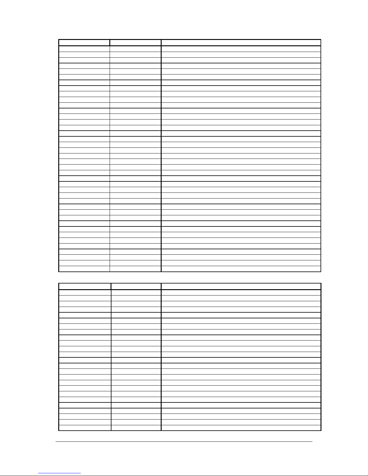
CN2 – Panel connector: HIROSE DG20G-40DP-1V (Matching type : DF20A-40DS-1C)
PIN SYMBOL DESCRIPTION
1 GND Ground
2 GND Ground
3 NC No connection
4 NC No connection
5 ER0 Even data bit R0
6 ER1 Even data bit R1
7 ER2 Even data bit R2
8 ER3 Even data bit R3
9 ER4 Even data bit R4
10 ER5 Even data bit R5
11 ER6 Even data bit R6
12 ER7 Even data bit R7
13 GND Ground
14 GND Ground
15 NC No connection
16 NC No connection
17 EG0 Even data bit G0
18 EG1 Even data bit G1
19 EG2 Even data bit G2
20 EG3 Even data bit G3
21 EG4 Even data bit G4
22 EG5 Even data bit G5
23 EG6 Even data bit G6
24 EG7 Even data bit G7
25 GND Ground
26 GND Ground
27 NC No connection
28 NC No connection
29 EB0 Even data bit B0
30 EB1 Even data bit B1
31 EB2 Even data bit B2
32 EB3 Even data bit B3
33 EB4 Even data bit B4
34 EB5 Even data bit B5
35 EB6 Even data bit B6
36 EB7 Even data bit B7
37 GND Ground
38 GND Ground
39 CLK Dot clock
40 NC No connection
CN3 – Panel connector: HIROSE DF20G-50DP-1V (Matching type : DF20A-50DS-1C)
PIN SYMBOL DESCRIPTION
1 GND Ground
2 GND Ground
3 NC No connection
4 NC No connection
5 OR0 Odd data bit R0
6 OR1 Odd data bit R1
7 OR2 Odd data bit R2
8 OR3 Odd data bit R3
9 OR4 Odd data bit R4
10 OR5 Odd data bit R5
11 OR6 Odd data bit R6
12 OR7 Odd data bit R7
13 GND Ground
14 GND Ground
15 NC No connection
16 NC No connection
17 OG0 Odd data bit G0
18 OG1 Odd data bit G1
19 OG2 Odd data bit G2
20 OG3 Odd data bit G3
21 OG4 Odd data bit G4
22 OG5 Odd data bit G5
23 OG6 Odd data bit G6
24 OG7 Odd data bit G7
25 GND Ground
Specifications subject to change without notice
© Digital View Ltd – Doc Ver 2.00: 15 November, 2017 Page
14 of 35
Page 15
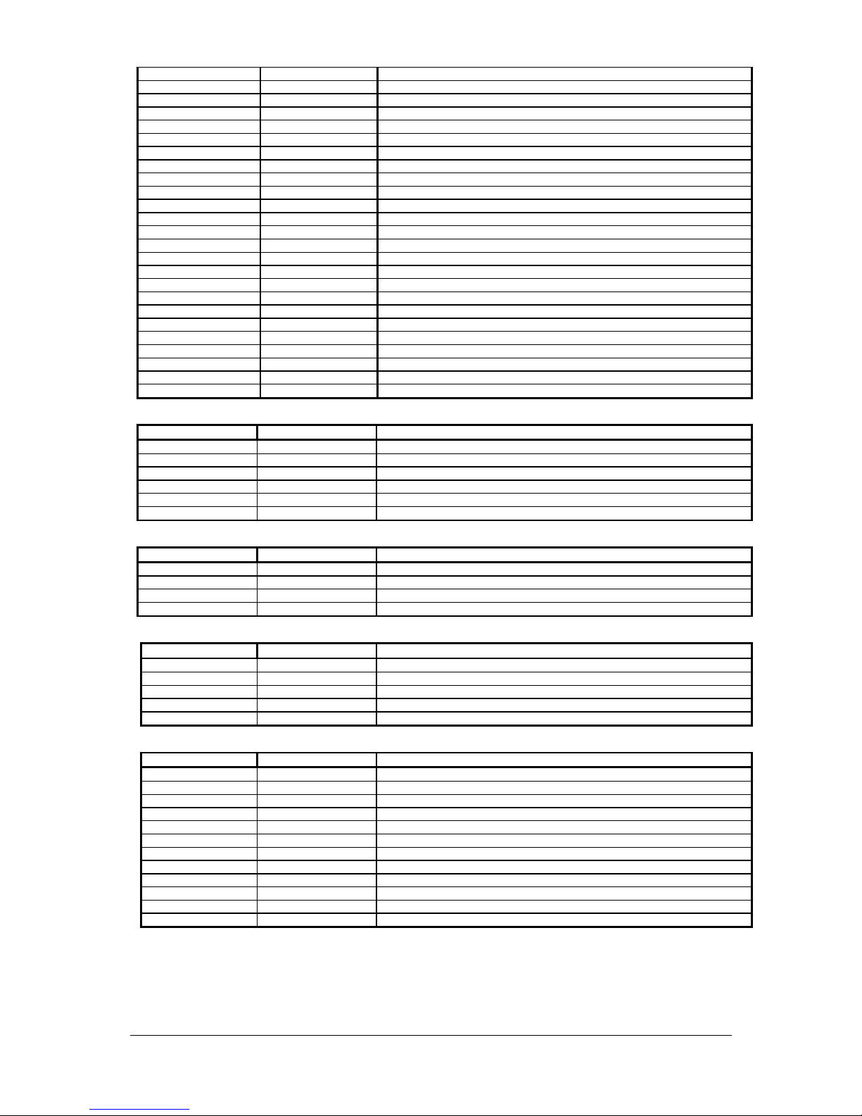
26 GND Ground
27 NC No connection
28 NC No connection
29 OB0 Odd data bit B0
30 OB1 Odd data bit B1
31 OB2 Odd data bit B2
32 OB3 Odd data bit B3
33 OB4 Odd data bit B4
34 OB5 Odd data bit B5
35 OB6 Odd data bit B6
36 OB7 Odd data bit B7
37 GND Ground
38 GND Ground
39 VS Vertical sync
40 CLK Dot clock
41 HS Horizontal sync
42 DE Display enable
43 PWR Power down control signal (5v TTL)
44 VLCD Panel power supply (3,3V/5V) (selected by JA3 & JA6)
45 VLCD Panel power supply (3,3V/5V) (selected by JA3 & JA6)
46 VLCD Panel power supply (3,3V/5V) (selected by JA3 & JA6)
47 NC No connection
48 VLCD12/18 +12V/18V panel supply (selected by JA3 & JA6)
49 VLCD12/18 +12V/18V panel supply (selected by JA3 & JA6)
50 VLCD12/18 +12V/18V panel supply (selected by JA3 & JA6)
CN8 – RS-232 serial control: JST B6B-XH-A compatible (Mating type : XHP-6 or compatible)
PIN SYMBOL DESCRIPTION
1 SDATA Reserved
2 SCLK Reserved
3 VCC +5V
4 TXD RS-232 Tx data
5 GND Ground
6 RXD RS-232 Rx data
CNA1 - Auxiliary power output: JST S4B-XH-A compatible (Mating type : XHP-4 or compatible)
PIN SYMBOL DESCRIPTION
1 AUX POWER +12V DC, 500mA max / +24V DC, 3A max
2 GND Ground
3 GND Ground
4 AUX 5V +5V DC, 500mA max
CNB1 – Backlight control connector: JST S5B-XH-A compatible (Mating type : XHP-5 or compatible)
PIN SYMBOL DESCRIPTION
1 GND Ground
2 VBKL Backlight power supply, +12VDC / +24V DC, 3A max
3 BLCTRL Backlight On/Off control signal (refer to JB2 & JB3)
4 BVR_WIP Backlight brightness VR pin WIP
5 BVR_A Backlight brightness VR pin A
CNC1 – OSD switch mount control, Hirose DF13-12P-1.25H compatible (Mating type : DF13-12S-1.25C or compatible)
PIN SYMBOL DESCRIPTION
1 PSWIN Power button A
2 SW_ON Power button B
3 BVR_A Backlight Brightness VR pin A
4 BVR_WIP Backlight Brightness R pin WIP
5 BVR_B Backlight Brightness VR pin B (470 ohm resistor to +5V Vcc)
6 GND Ground
7 MENU OSD menu
8 -/LEFT OSD -/Left
9 +/RIGHT OSD +/Right
10 SEL_DN OSD Select down
11 SEL_UP OSD Select up
12 NC No connection
The VR for brightness depends on the backlight driver. The main power load for On/Off is handled by a relay on the
controller.
Specifications subject to change without notice
© Digital View Ltd – Doc Ver 2.00: 15 November, 2017 Page
15 of 35
Page 16
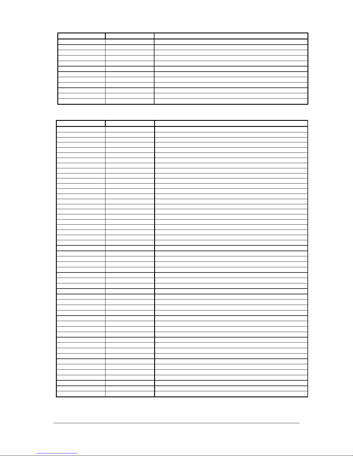
CNC1 – OSD switch mount control, Hirose DF13A-12P-1.25H compatible (Mating type : DF13-12S-1.25C)
PIN SYMBOL DESCRIPTION
1 PSWIN Power button A
2 SW_ON Power button B
3 BVR_A Backlight Brightness VR pin A
4 BVR_WIP Backlight Brightness R pin WIP
5 BVR_B Backlight Brightness VR pin B (470 ohm resistor to +5V Vcc)
6 GND Ground
7 MENU OSD menu
8 -/LEFT OSD -/Left
9 +/RIGHT OSD +/Right
10 SEL_DN OSD Select down
11 SEL_UP OSD Select up
12 NC No connection
J1 – LVDS output connector: STARCONN : 115E51-0000RA-M3-R (Matching type : STARCONN 107D51-000001-00 or
compaible)
PIN SYMBOL DESCRIPTION
1 VLCD_HV Panel power supply (+12V / 18V) (selected by JA3 & JA6)
2 VLCD_HV Panel power supply (+12V / 18V) (selected by JA3 & JA6)
3 VLCD_HV Panel power supply (+12V / 18V) (selected by JA3 & JA6)
4 VLCD_HV Panel power supply (+12V / 18V) (selected by JA3 & JA6)
5 VLCD_HV Panel power supply (+12V / 18V) (selected by JA3 & JA6)
6 VLCD_LV Panel power supply (3,3V/5V) (selected by JA3 & JA6)
7 VLCD_LV
8 VLCD_LV
9 VLCD_LV
10 VLCD_LV
11 GND Ground
12 GND Ground
13 GND Ground
14 GND Ground
15 GND Ground
16 NC No function
17 NC No function
18 NC No function
19 NC No function
20 GND Ground
21 GND Ground
22 NC No function
23 NC No function
24 LVDS_OUT1_A3+ Positive differential LVDS data bit A3
25 LVDS_OUT1_A3- Negative differential LVDS data bit A3
26 GND Ground
27 LVDS_OUT1_AC+ Positive LVDS clock for A channel
28 LVDS_OUT1_AC- Negative LVDS clock for A channel
29 GND Ground
30 LVDS_OUT1_A2+ Positive differential LVDS data bit A2
31 LVDS_OUT1_A2- Negative differential LVDS data bit A2
32 LVDS_OUT1_A1+ Positive differential LVDS data bit A1
33 LVDS_OUT1_A1- Negative differential LVDS data bit A1
34 LVDS_OUT1_A0+ Positive differential LVDS data bit A0
35 LVDS_OUT1_A0- Negative differential LVDS data bit A0
36 GND Ground
37 NC No function
38 NC No function
39 LVDS_OUT1_B3+ Positive differential LVDS data bit B3
40 LVDS_OUT1_B3- Negative differential LVDS data bit B3
41 GND Ground
42 LVDS_OUT1_BC+ Positive LVDS clock for B channel
43 LVDS_OUT1_BC- Negative LVDS clock for B channel
44 GND Ground
45 LVDS_OUT1_B2+ Positive differential LVDS data bit B2
46 LVDS_OUT1_B2- Negative differential LVDS data bit B2
47 LVDS_OUT1_B1+ Positive differential LVDS data bit B1
48 LVDS_OUT1_B1- Negative differential LVDS data bit B1
49 LVDS_OUT1_B0+ Positive differential LVDS data bit B0
50 LVDS_OUT1_B0- Negative differential LVDS data bit B0
51 GND Ground
Specifications subject to change without notice
© Digital View Ltd – Doc Ver 2.00: 15 November, 2017 Page
Panel power supply (3,3V/5V) (selected by JA3 & JA6)
Panel power supply (3,3V/5V) (selected by JA3 & JA6)
Panel power supply (3,3V/5V) (selected by JA3 & JA6)
Panel power supply (3,3V/5V) (selected by JA3 & JA6)
16 of 35
Page 17
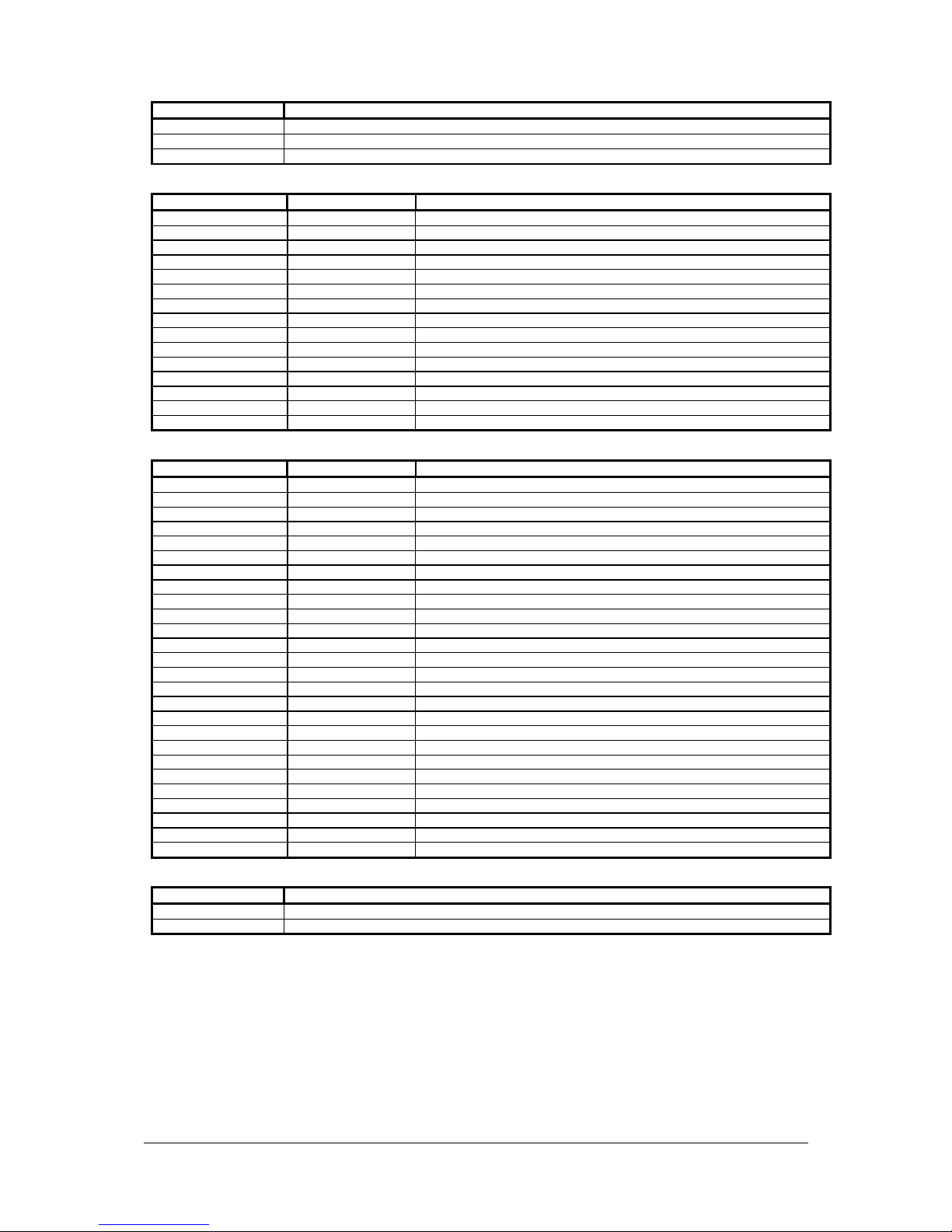
LED1 – Dual color Status LED connector: JST 3-way, B3B-XH-A compatible (Mating type : XHP-3 or compatible)
PIN DESCRIPTION
1 Green LED pin (anode)
2 LED pin common (cathode)
3 Red LED pin (anode)
P1 - Analog VGA input – DB-15 way high density 3 row
PIN SYMBOL DESCRIPTION
1 PCR Red, analog
2 PCG Green, analog
3 PCB Blue analog
4 ID2 Reserved for monitor ID bit 2 (grounded)
5 DGND Digital ground
6 AGND Analog ground red
7 AGND Analog ground green
8 AGND Analog ground blue
9 DDC_5V +5V power supply for DDC (optional)
10 DGND Digital ground
11 ID0 Reserved for monitor ID bit 0 (grounded)
12 DDC_SDA DDC serial data
13 HS_IN Horizontal sync or composite sync, input
14 VS_IN Vertical sync, input
15 DDC_SCL DDC serial clock
P2 – DVI-D input
PIN SYMBOL DESCRIPTION
1 /RX2 TMDS Data 2-
2 RX2 TMDS Data 2+
3 GND Digital Ground
4 NC No connection
5 NC No connection
6 DVI_DDC_CLK DDC Clock
7 DVI_DDC_DAT DDC Data
8 DVI_VS_IN Analog vertical Sync
9 /RX1 TMDS Data 110 RX1 TMDS Data 1+
11 GND Digital Ground
12 NC No connection
13 NC No connection
14 DVI_DDC_5V +5V power supply for DDC (optional)
15 GND Ground (+5, Analog H/V Sync)
16 NC No connection
17 /RX0 TMDS Data 018 RX0 TMDS Data 0+
19 GND Digital Ground
20 NC No connection
21 NC No connection
22 GND Digital Ground
23 RXC TMDS Clock+
24 /RXC TMDS Clock25 NC No connection
26 NC No connection
PP2 - Power supply Molex 43650-0200 compatible (Mating type : Molex 43645-0200 compatible)
PIN DESCRIPTION
1 +12VDC 5A max / +24VDC 5A max
2 Ground
Specifications subject to change without notice
© Digital View Ltd – Doc Ver 2.00: 15 November, 2017 Page
17 of 35
Page 18
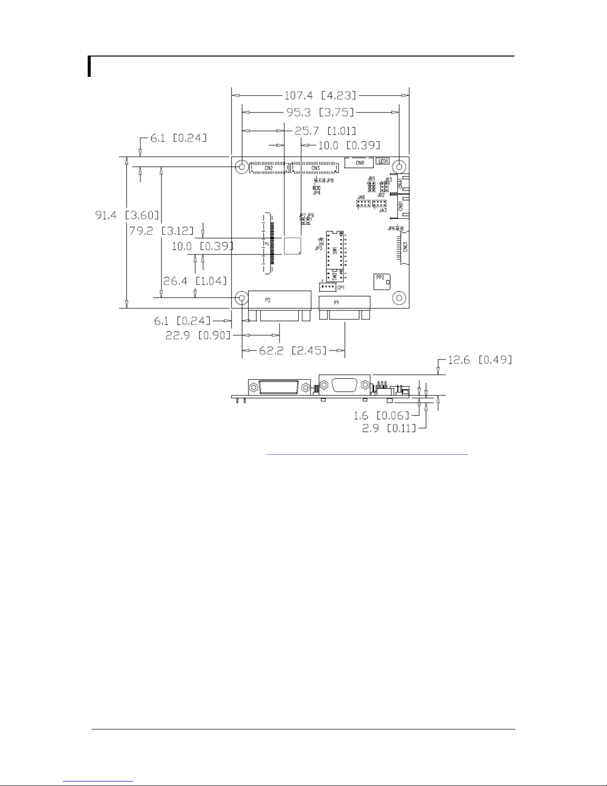
CONTROLLER DIMENSIONS
Ready-made 3D Pro-E (SLDPRT) drawing files - Save time and effort for your system volumetric analysis design.
Includes jpg file previews. Please go to download at http://www.digitalview.com/products/he-1400v2-lcd-controller
The maximum thickness of the controller is 15.8mm (measured from bottom of PCB to top of components, including
any underside components & leads). We recommend clearances of:
• 5mm from bottom of PCB - if mounting on a metal plate we also recommend a layer of suitable insulation
material is added to the mounting plate surface.
• 10mm above the components
• 3~5mm around the edges
Any of the holes shown above can be used for mounting the PCB, they are 3.2mm in diameter.
CAUTION: Ensure adequate insulation is provided for all areas of the PCB with special attention to high
voltage parts such as the backlight driver.
Specifications subject to change without notice
© Digital View Ltd – Doc Ver 2.00: 15 November, 2017 Page
18 of 35
Page 19
APPLICATION NOTES
USING THE CONTROLLER WITHOUT BUTTONS ATTACHED
This is very straightforward by following the steps below :
• Firstly setup the controller/display system with the buttons. With controls attached and display system active make any
settings for colour and image position as required then switch everything off.
• Use a jumper to close JP6 jumper, this will fix the board On.
• Refer to backlight driver specifications for details as to fixing brightness to a desired level, this may require a resistor, an
open circuit or closed circuit depending on backlight driver.
BACKLIGHT DRIVER CONNECTION
There are potentially 3 issues to consider with backlight driver connection:
• Power
• Enable
• Brightness
Please read the following sections for a guide to these issues.
Backlight Power: As per the table for CNB1 pin 1 is ground and pin 2 provides DC12V/ 24V DC . This should be matched
with the backlight driver specification: see table.
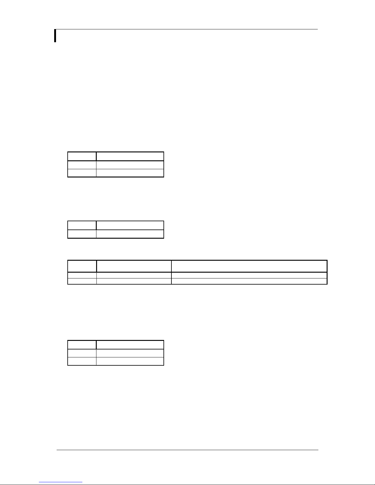
CNB1
PIN DESCRIPTION
1 Ground
2 +12VDC / 24VDC
Remark: For higher power backlight driver, more current (for 12V / 24V) can be taken from CNA1 pin 1.
Maximum current drawn on CNA1 pin 1 and CNB1 pin 2 is 3A (24V) / 3A(12V)
Enable: This is a pin provided on some backlight drivers for On/Off function and is used by this panel controller for VESA
DPMS compliance. If the backlight driver does not have an enable pin or the enable pin is not used then DPMS will not be
operational. Pin 3 should be matched to the backlight drivers specification for the ‘enable’ or ‘disable’ pin.
CNB1
PIN DESCRIPTION
3 Enable
Further, jumpers JB2 & JB3 should be set to match the backlight drivers specification for the enable pin power and High or
Low setting: see table.
Ref
JB2 Backlight enable voltage 1-2 H = 3.3V, 2-3 H = 5V (Vcc), OPEN H = open collector
JB3 Backlight on/off polarity control 1-2 H = On, 2-3 L = On
Brightness: There are various methods for brightness control and it is important to consider the specifications for the backlight
driver to be used. Generally the situation is:
• Brightness can controlled by using a resistor or VR (Variable Resistor).
• Brightness controlled by adding a circuit such as PW M (Pulse Width Modulation).
• No adjustment of brightness is possible.
CNB1 pins 4 & 5 are available for connecting to an backlight driver or circuit where VR control is supported.
CNB1
PIN DESCRIPTION
4 VR WIP
5 VR A
This can then be matched with function controls (OSD switch mount) pins 3 & 4: see cable design below .
Purpose Note
Specifications subject to change without notice
© Digital View Ltd – Doc Ver 2.00: 15 November, 2017 Page
19 of 35
Page 20
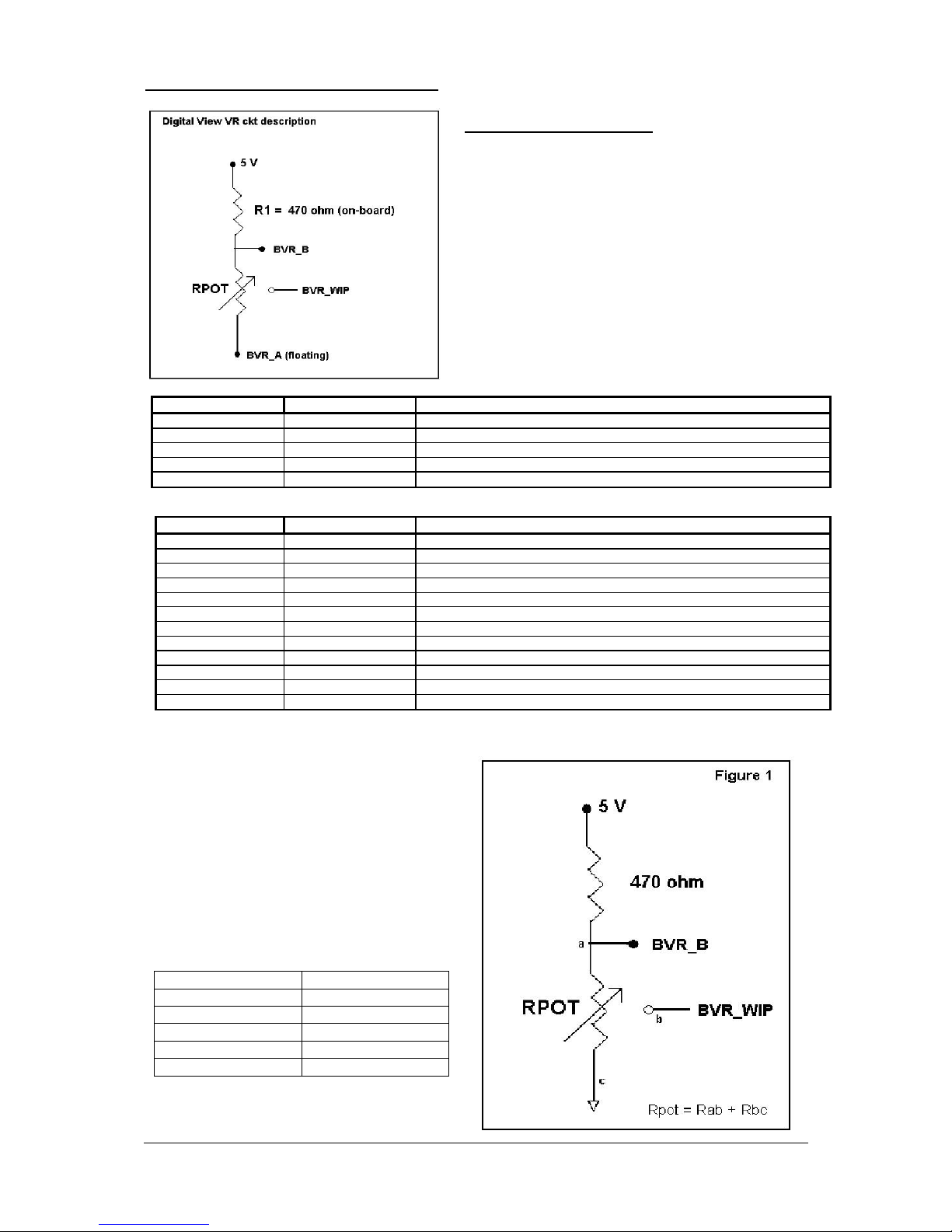
Design Guideline for making VR circuitry :
available at CNC1 pin 6).
5 K 2.4 V
Signal description / Notes :
1) R1 : 470ohm on board
2) RPOT is an external potentiometer (in-line dip
style) that can be plugged directly into CNC1 pins
3,4,5. RPOT must be supplied / installed by user.
3) BVR_B : Voltage tapped from “top” of
potentiometer, the node of R1 and RPOT.
4) BVR_WIP : Voltage tapped from wiper arm of
RPOT.
5) BVR_A : Voltage tapped from “bottom” of
RPOT.
Note : BVR_A voltage is left floating on the
controller board. To use this circuit, you need
to tie this point to a potential (usually GND,
CNB1 – Backlight control connector: JST B5B-XH-A (Matching type : XHP-5)
PIN SYMBOL DESCRIPTION
1 GND Ground
2 VBKL +12VDC / 24VDC, backlight power supply (selected by JA3 & JA6)
3 BLCTRL On/Off control (enable) – see JB2 & JB3
4 BVR_WIP Brightness VR - WIP
5 BVR_A Brightness VR A
CNC1 – Control switch, JST B12B-XH-A (Matching type : XHP-12)
PIN SYMBOL DESCRIPTION
1 PSWIN Power button A
2 SW_ON Power button B
3 BVR_A Backlight Brightness VR pin A
4 BVR_WIP Backlight Brightness R pin WIP
5 BVR_B Backlight Brightness VR pin B (470 ohm resistor to +5V Vcc)
6 GND Ground
7 MENU OSD menu
8 -/LEFT OSD -/Left
9 +/RIGHT OSD +/Right
10 SEL_DN OSD Select down
11 SEL_UP OSD Select up
12 NC No connection
The VR for brightness depends on the backlight driver.The main power load for On/Off is handled by a relay on the ontroller.
Example for circuit design :
1.)Choose RPOT = 10K
2.) Tie BVR_A to GND
3.) Circuit analysis gives BVR_WIP as the
following (see Figure 1)
BVR_WIP = 5 x (Rbc/10.47)
where BVR_WIP is in Volts.
And Rbc is the resistance from the wiper arm
to bottom of pot in Kohms.
To evaluate, plug in different values of Rbc :
Rbc BVR_WIP
0 0 V
2.5 K 1.2 V
7.5 K 3.6 V
10 K 4.8 V
So this circuit could provide Brightness adjust
voltage ranging from 0V to 5V.
Specifications subject to change without notice
© Digital View Ltd – Doc Ver 2.00: 15 November, 2017 Page
20 of 35
Page 21

TROUBLESHOOTING
General
A general guide to troubleshooting a flat panel display system it is worth considering the system as separate elements, such
as:
Controller (jumpers, PC settings)
Panel (controller, cabling, connection, panel, PC settings)
Backlight (backlight driver, cabling, backlight tubes)
Cabling
Computer system (display settings, operating system)
Through step by step cross checking with instruction manuals and a process of elimination to isolate the problem it is usually
possible to clearly identify the problem area.
No image:
If the panel backlight is not working it may still be possible to just see some image on the display.
A lack of image is most likely to be caused by incorrect connection, lack of power, failure to provide a signal or incorrect
graphic card settings.
Image position:
If it is impossible to position the image correctly, ie the image adjustment controls will not move the image far enough, then
test using another graphics card. This situation can occur with a custom graphics card that is not close to standard timings or if
something is in the graphics line that may be affecting the signal such as a signal splitter (please note that normally a signal
splitter will not have any adverse effect).
Image appearance:
A faulty panel can have blank lines, failed sections, flickering or flashing display
Incorrect graphics card refresh rate, resolution or interlaced mode will probably cause the image to be the wrong size, to
scroll, flicker badly or possibly even no image.
Incorrect jumper settings on the controller may cause everything from total failure to incorrect image. CAUTION: Do not
set the panel power input incorrectly.
Sparkling on the display: faulty panel signal cable.
Backlight:
Items to check include: Power input, Controls, backlight drivers and Tubes generally in this order.
If half the screen is dimmer than the other half:
Check cabling for the backlight driver.
For a specific backlight tube check the AC pins orientation (CAUTION: Never reverse any DC power pins).
Also:
If adjusting brightness control has no effect the chances are that the VR rating or method of adjusting brightness is not
compatible or correctly connected to the backlight driver.
If system does not power down when there is a loss of signal
Continued failure:
If unit after unit keeps failing consider and investigate whether you are short circuiting the equipment or doing something else
seriously wrong.
Generally after common sense issues have been resolved we recommend step by step substitution of known working parts to
isolate the problem.
Specifications subject to change without notice
© Digital View Ltd – Doc Ver 2.00: 15 November, 2017 Page
21 of 35
Page 22
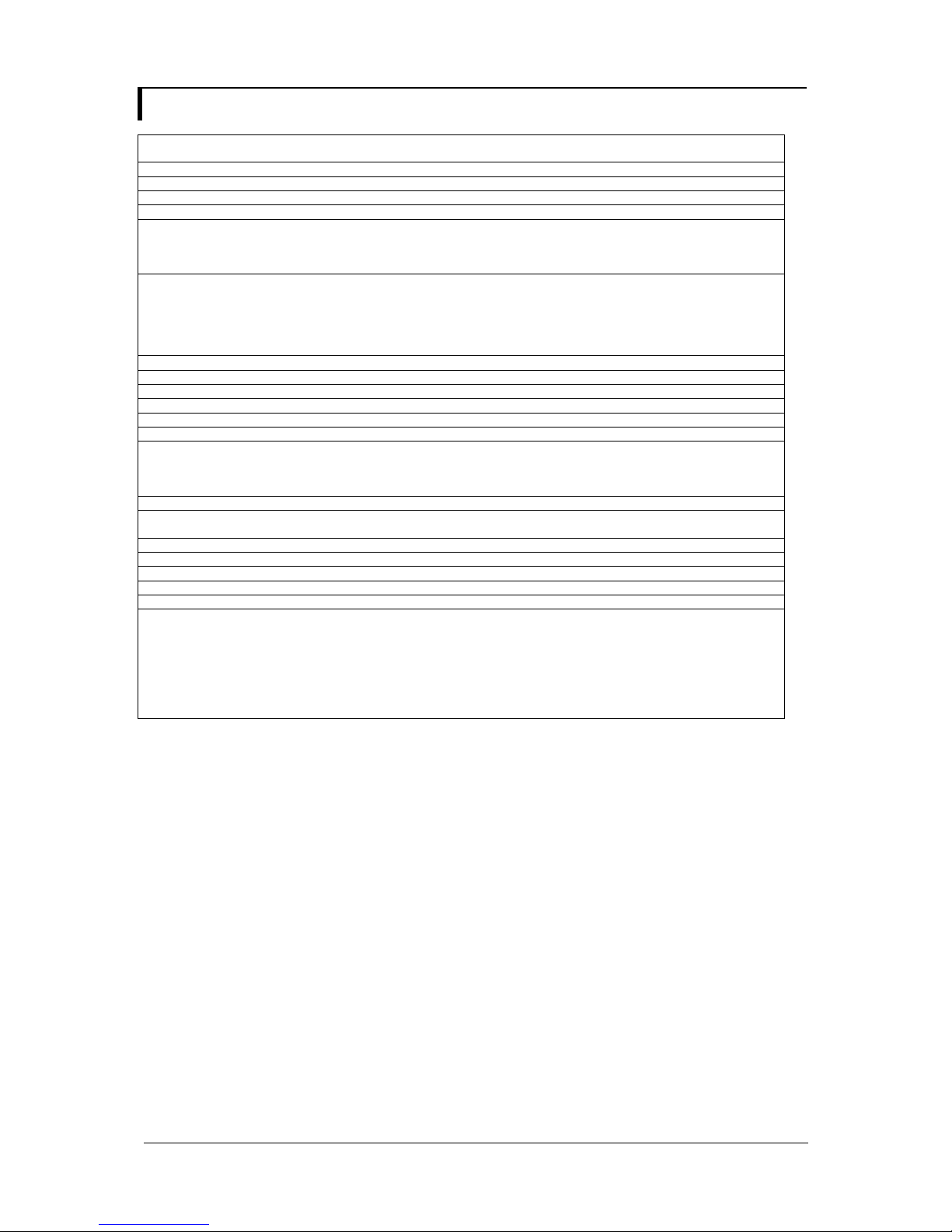
SPECIFICATIONS
Panel compatibility 1440x900, 1366x768, 1280x1024, 1280x800, 1024x768, 800x600, 640x480
No. of colours Up to 3 x 8 bit providing 16.7 million colours.
Vertical refresh rate SXGA, XGA, SVGA, VGA resolution up to 60Hz.
Dot clock (pixel clock) maximum 135 MHz
Graphics formats Up to 1440x900 (refer to Appendix I)
Standard input at source - VGA analog (15-pin) standard with automatic detection of :
Controls available - On/Off
Control interface - Buttons
Settings memory Settings are stored in non volatile memory
Language OSD support Yes
Graphics OSD icons Yes
VESA DPMS implementation Yes
Plug & Play VESA DDC 1, 2/b compatible
Voltage output for LCD +3.3V , +5V, +12V, +18V
Input voltage 12VDC , 5A max / 24VDC 5A max +/- 5%
Controller power consumption Approx 2.5W(controller logic only, no panel and backlight driver are
Controller dimensions 107.4mm x 91.4mm x 17.1mm
Storage temperature limits -40oC to +85oC
Operating temperature limits -20oC to +80oC**
Coating HumiSeal 1B73 Acrylic Conformal Coating
Calculated Mean Time Between Failures In excess of 100,000 hours
Use of memory on board - 1 pc SRAM - (MCU, TSUMU58VHN-1) on U13, 15.75Kbytes which is a
** Overall suitability for usage in critical applications must be independently tested and verified by the user.
NOTES
Please note the following:
• For specific panel setup a sample of an LCD may be required (this will be returned) and a copy of the full technical
specifications for the panel from the manufacturer.
• Relayout and custom development services are available.
resolution TFT LVDS or TTL LCD’s support.
Digital Separate Sync
Sync On Green
- DVI-D
- Brightness (backlight)
- OSD menu
- OSD select
- OSD setting +
- OSD setting -
The current drawn for 18V panel from 24VDC power input is limited to 2A.
The current drawn for 3.3V, 5V or 12V panel from 12V/24VDC power input is
limited to 3A.
involved)
volatile memory : SRAM for OSD.
- 1 pc Flash - (GDQ40CTIGR) on U10, 4Mbits which is a non-volatile
memory for system program.
- 1 pc EEPROM - (24C02N) on U14, 2KBits which is a non-volatile memory
for VGA EDID.
- 1 pc EEPROM- (24C02N) on U15, 2Kbits which is a non-volatile memory
for DVI EDID.
Specifications subject to change without notice
© Digital View Ltd – Doc Ver 2.00: 15 November, 2017 Page
22 of 35
Page 23
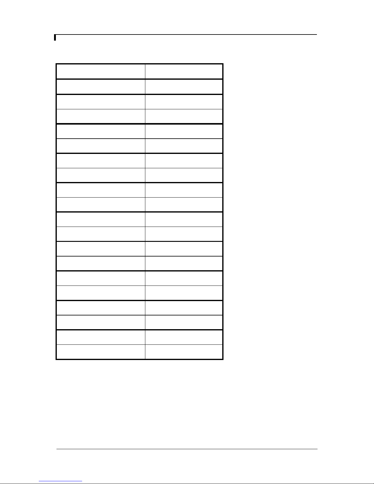
Appendix I – Mode Support Table
VGA port :
Resolution Sync Mode
640x480 60Hz Digital Separate Sync
800x600 56Hz Digital Separate Sync
800x600 56Hz Sync On Green
800x600 60Hz Digital Separate Sync
800x600 60Hz Sync On Green
1024x768 60Hz Digital Separate Sync
1024x768 60Hz Sync On Green
1280x768 60Hz Digital Separate Sync
1280x768 60Hz Sync On Green
1280x800 60Hz Digital Separate Sync
1280x800 60Hz Sync On Green
1280x1024 60Hz Digital Separate Sync
1280x1024 60Hz Sync On Green
1360x768 60Hz Digital Separate Sync
1360x768 60Hz Sync On Green
1366x768 60Hz Digital Separate Sync
1366x768 60Hz Sync On Green
1440x900 60Hz Digital Separate Sync
1440x900 60Hz Sync On Green
Specifications subject to change without notice
© Digital View Ltd – Doc Ver 2.00: 15 November, 2017 Page
23 of 35
Page 24
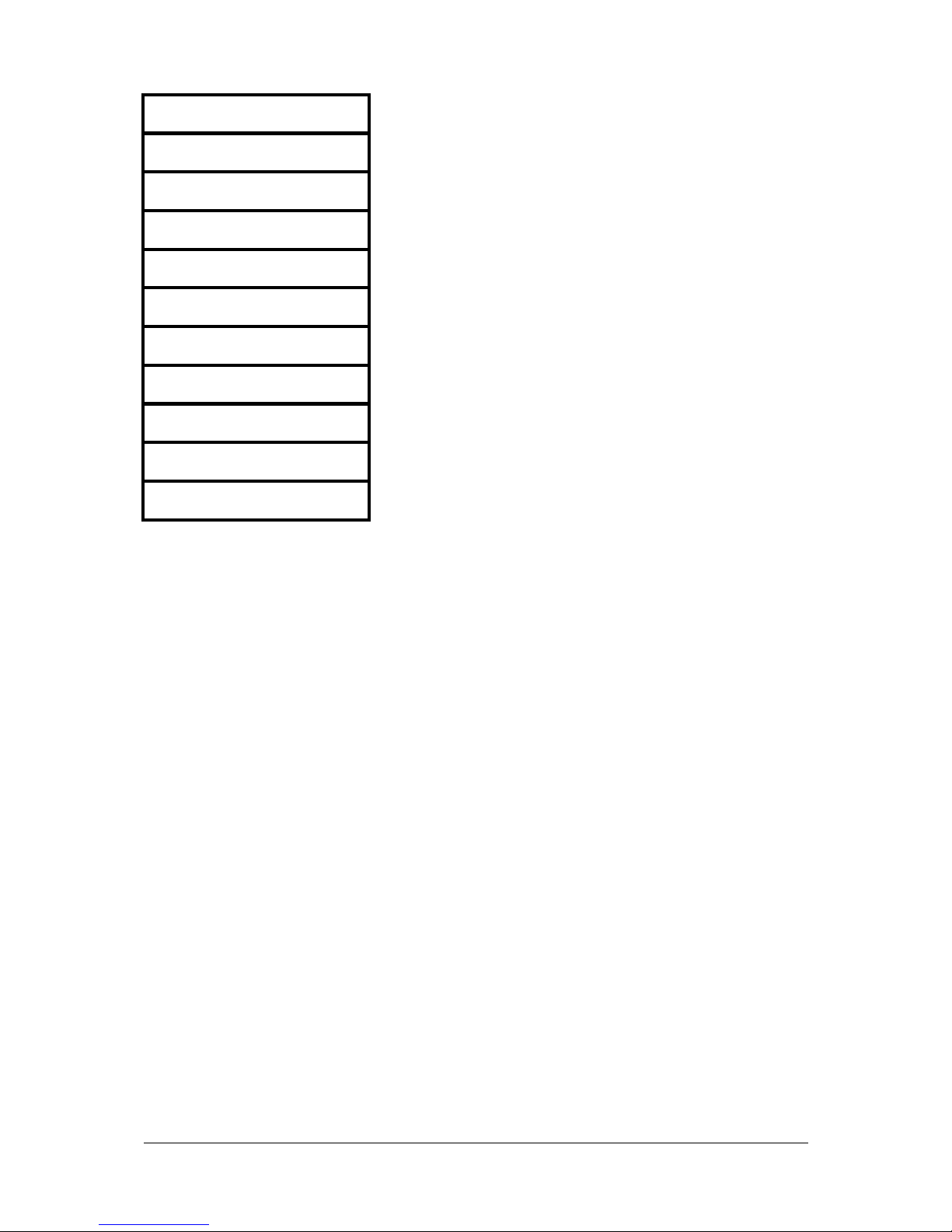
DVI port :
Resolution
640x480 60Hz
800x600 56Hz
800x600 60Hz
1024x768 60Hz
1280x768 60Hz
1280x800 60Hz
1280x1024 60Hz
1360x768 60Hz
1366x768 60Hz
1440x900 60Hz
Remark :
The controller has been designed to take a very wide range of input signals however to optimize the PC’s graphics
performance we recommend choosing 60Hz vertical refresh rate. To support on higher refresh rate over 60Hz, the LCD panel
may not support.
Specifications subject to change without notice
© Digital View Ltd – Doc Ver 2.00: 15 November, 2017 Page
24 of 35
Page 25
Function
Command
Description
Acknowledge (if enabled)
“?”
Query
Default:
“8””0”
5
4
9
1
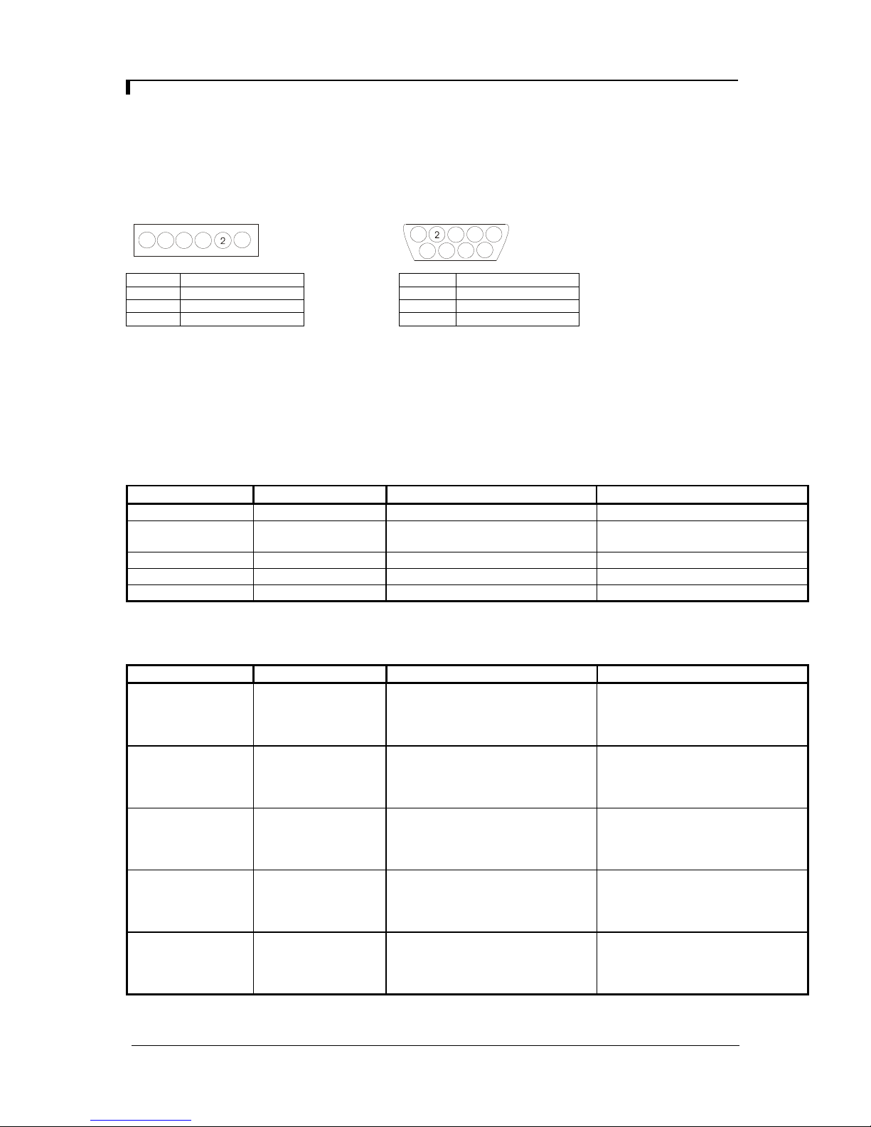
Appendix II – RS-232 control protocols
RS-232 Serial control (Baud rate 2400,
Physical connection :
Controller side Computer side
Connector interface : CN8 Connector interface : Serial port
Mating connector : JST XHP-6 Mating connector : DB9 Female
5 463
PIN# Description PIN# Description
4 RS-232 Tx Data 2 RS-232 Rx Data
5 Ground 3 RS-232 Tx Data
6 RS-232 Rx Data 5 Ground
Remark :
(1) : RS-232 connection cable, 600mm P/N 426090200-3 can be ordered separately for connection.
Software connection :
The OSD function can be controlled through sending the RS-232 protocol.
The RS-232 program can be custom-made to fit for application or it can be used the program provided by Digitalview on
request. Please contact your local sales for informations.
Mating face of CN8 Mating face of RS-232 DB9 Male
8 bits, 1 stop bit and no parity
)
1
3
8
7
6
1. Commands to implement switch mount control buttons
Function Command Description Acknowledge (if enabled)
Menu 0xf7 Menu button pressed Button equivalent
Select-down
0xfa Select down button pressed Button equivalent
button
Select-up button 0xfb Select up button pressed Button equivalent
Right/+ button 0xfc Right/+button pressed Button equivalent
Left/- button 0xfd Left/- button pressed Button equivalent
2. Parameter setting - immediate, relative, reset and query
Brightness control 0x81,
nn | “+” | “-” |
“r” | “R” |
Contrast control 0x82, “a” | “A”,
nn | “+” | “-” |
“r” | “R” |
“?”
Phase # 0x85,
nn | “+” | “-” |
“?”
Set brightness =
value/increment/decrement
Reset
Set all contrast =
value/increment/decrement
Reset
Query
Set dot clock phase =
value/increment/decrement
Query
Brightness.
Range: “0””0”-“F””F”
Contrast.
Range: “0””0”-“F””F”
Default: “8””0”
Dot clock phase.
(In VGA mode only)
Image H position # 0x86,
nn | “+” | “-” |
“?”
Set img_hpos =
value/increment/decrement
Query
Image horizontal position.
(In VGA mode only)
Image V position # 0x87,
nn | “+” | “-” |
“?”
Set img_vpos =
value/increment/decrement
Query
Image vertical position.
(In VGA mode only)
Specifications subject to change without notice
© Digital View Ltd – Doc Ver 2.00: 15 November, 2017 Page
25 of 35
Page 26
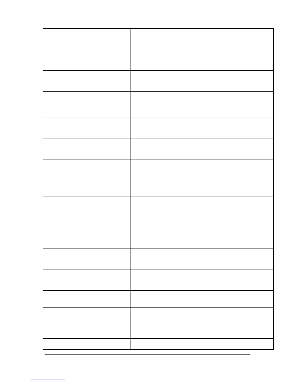
Sharpness 0x8a,
n | “+” | “-” |
“r” | “R” |
“?”
Set sharpness =
value/increment/decrement
Reset
Query
Sharpness.
“0x30” – 0 (Default)
“0x31” – 1
“0x32” – 2
“0x33” – 3
“0x34” – 4
“0x35” – 5
“0x36” – 6
Clock # 0x8b,
nn | “+” | “-“ |
“?”
Set H active size =
value/increment/decrement
Query
Frequency adjustment
(In VGA mode only)
Scaling Mode 0x8c,
n |
“r” | “R” |
“?”
Set graphic image scaling mode
=
value
Reset
Image expansion on/off.
“0x31” – Wide (Fill Screen)
“0x39” – 4:3
Query
OSD H position 0x90,
nnn | “+” | “-“ | “r” |
“R” | “?”
OSD V position 0x91,
nnn | “+” | “-“ | “r” |
“R” | “?”
OSD
Transparency
0x92,
n
“r” | “R” |
“?”
Set osd_hpos =
value/increment/decrement
Reset
Query
Set osd_vpos =
value/increment/decrement
Reset
Query
Set OSD transparency =
value/increment/decrement
Reset
Query
OSD horizontal position
Range: “0””0””0”-“0””6””4”
Default: “0””3””2”
OSD vertical position
Range: “0””0””0”-“0””6””4”
Default: “0””3””2”
OSD transparency.
“0x30” – 0 (Default)
“0x31” – 25
“0x32” – 50
“0x33” – 75
“0x34” – 100
OSD menu
timeout
0x93,
nn | “+” | “-” |
“r” | “R” |
“?”
Select menu timeout =
value/increment/decrement
Reset
Query
OSD menu timeout value. If
value > max available step, set it
to the max available step.
“0x30,0x30” – 0 (Always on)
“0x30,0x41” – 10 sec (Default)
“0x31,0x34” – 20 sec
“0x31,0x45” – 30 sec
“0x32,0x38” – 40 sec
“0x33,0x32” – 50 sec
“0x33,0x43” – 60 sec
Select OSD
language
Input main select
* Function in valid
mode only
Auto Source Seek 0x99,
GAMMA value
select
0x95,
n |
“r” | “R” |
“?”
0x98,
nn | “+” | “-“ | “r” |
“R” | “?”
“0” | “1” |
“?” |
0x9d,
n |
“r” | “R”
“?”
Select language =
English, French,…
Reset
Query
Select input main =
PC or video or next available
Reset
Query
Disable/ Enable
Query
Select GAMMA value =
Value
Reset
Query
"0x30" – English (Default)
“0x32” - French
“0x33” – Spanish
Main selected.
“0x41,0x31” VGA (Default)
“0x46,0x31” DVI
"0x30" – Disable
"0x31" – Enable (Default)
GAMMA value:
“0x35” – 1.8,
“0x37” – 2.0
“0x32” – 2.2 (Default),
“0x41” – 2.4
“0x43” – 2.6
Colour
temperature select
Specifications subject to change without notice
© Digital View Ltd – Doc Ver 2.00: 15 November, 2017 Page
0xb3,
n |
Select colour temperature =
value
Main selected.
“0” – user defined RGB values.
26 of 35
Page 27
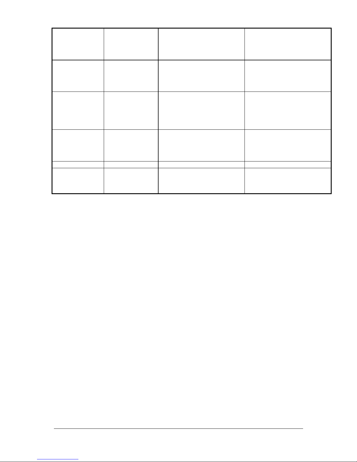
Red level for
OSD turn off
0xbd
Turn off the OSD
“1” -
successful
selected colour
temperature
Green level for
selected colour
temperature
Blue level for
selected colour
temperature
“r” | “R” |
“?”
0xb4,
nn | “+” | “-” |
“r” | “R” |
“?”
0xb5,
nn | “+” | “-” |
“r” | “R” |
“?”
0xb6,
nn | “+” | “-” |
“r” | “R” |
“?”
Reset
Query
Set the level of the red channel
for the selected colour temp. =
value/increment/decrement
Reset
Query
Set the level of the green
channel for the selected colour
temp. =
value/increment/decrement
Reset
Query
Set the level of the blue channel
for the selected colour temp. =
value/increment/decrement
Reset
Query
“1” – 4200K.
“2” – 5000K.
“3” – 6500K.
“4” – 7500K. (Default)
“5” – 9300K.
Red level for selected colour
temperature.
Range: “0””0”-“F””F”
Default: “8””0”
Green level for selected colour
temperature.
Range: “0””0”-“F””F”
Default: “8””0”
Blue level for selected colour
temperature.
Range: “0””0”-“F””F”
Default: “8””0”
Wide Screen
Mode Selection
0xd9,
“0” | “1”| “2” | “3”
“r” | “R”
“?”
Wide Screen Mode
Reset
Query
“0” – 1280x768
“1” – 1360x768
“2” – 1366x768
"3" – 1368x768
Specifications subject to change without notice
© Digital View Ltd – Doc Ver 2.00: 15 November, 2017 Page
27 of 35
Page 28
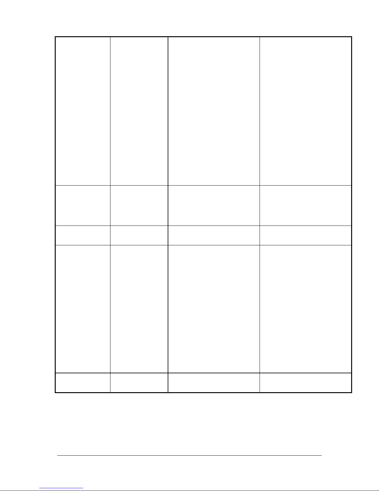
Backlight
brightness control
0xe0,
nn | “+” | “-” |
“r” | “R” |
“?”
Set backlight brightness =
value/increment/decrement
Reset
Query
Backlight brightness.
Range:
D/A : “0””0”-“6””4”
100Hz : “0””0” ~ “6””4”
120Hz : “0””0” ~ “6””4”
140Hz : “0””0” ~ “6””4”
160Hz : “0””0” ~ “6””4”
180Hz : “0””0” ~ “6””4”
200Hz : “0””0” ~ “6””4”
220Hz : “0””0” ~ “6””4”
240Hz : “0””0” ~ “6””4”
260Hz : “0””0” ~ “6””4”
280Hz : “0””0” ~ “6””4”
300Hz : “0””0” ~ “6””4”
320Hz : “0””0” ~ “6””4”
340Hz : “0””0” ~ “6””4”
360Hz : “0””0” ~ “6””4”
380Hz : “0””0” ~ “6””4”
400Hz : “0””0” ~ “6””4”
420Hz : “0””0” ~ “6””4”
440Hz : “0””0” ~ “6””4”
Backlight on/off
control
Backlight D/A or
PWM selection
Backlight PWM
Frequency
Backlight Invert 0xe7,
0xe1,
“0” |
“1” |
“r” | “R” |
“?”
0xe5,
“0” | “1” |
“?”
0xe6,
nnn | “+” | “-” |
“?”
0” | “1” |
“?”
Set backlight brightness =
Disable backlight
Enable backlight
Reset
Query
Backlight working status
Set: PWM or D/A
Query
Set Backlight PWM Frequency =
Value/ increment/ decrement
Query
Set On or Off
Query
Backlight on/off.
“1” = normal (Default)
“1” – PWM
“0” – D/A
+/- 20Hz
Value
100Hz : “0”, “6”, “4”
120Hz : “0”, “7”, “8”
140Hz : “0”, “8”, “C”
160Hz : “0”, “A”, “0”
180Hz : “0”, “B”, “4”
200Hz : “0”, “C”, “8”
220Hz : “0”, “D”, “C”
240Hz : “0”, “F”, “0”
260Hz : “1”, “0”, “4”
280Hz : “1”, “1”, “8”
300Hz : “1”, “2”, “C”
320Hz : “1”, “4”, “0”
340Hz : “1”, “5”, “4”
360Hz : “1”, “6”, “8”
380Hz : “1”, “7”, “C”
400Hz : “1”, “9”, “0”
420Hz : “1”, “A”, “4”
440Hz : “1”, “B”, “8”
“1” – Invert
“0” – Normal
# - Function in VGA mode only
Specifications subject to change without notice
© Digital View Ltd – Doc Ver 2.00: 15 November, 2017 Page
28 of 35
Page 29
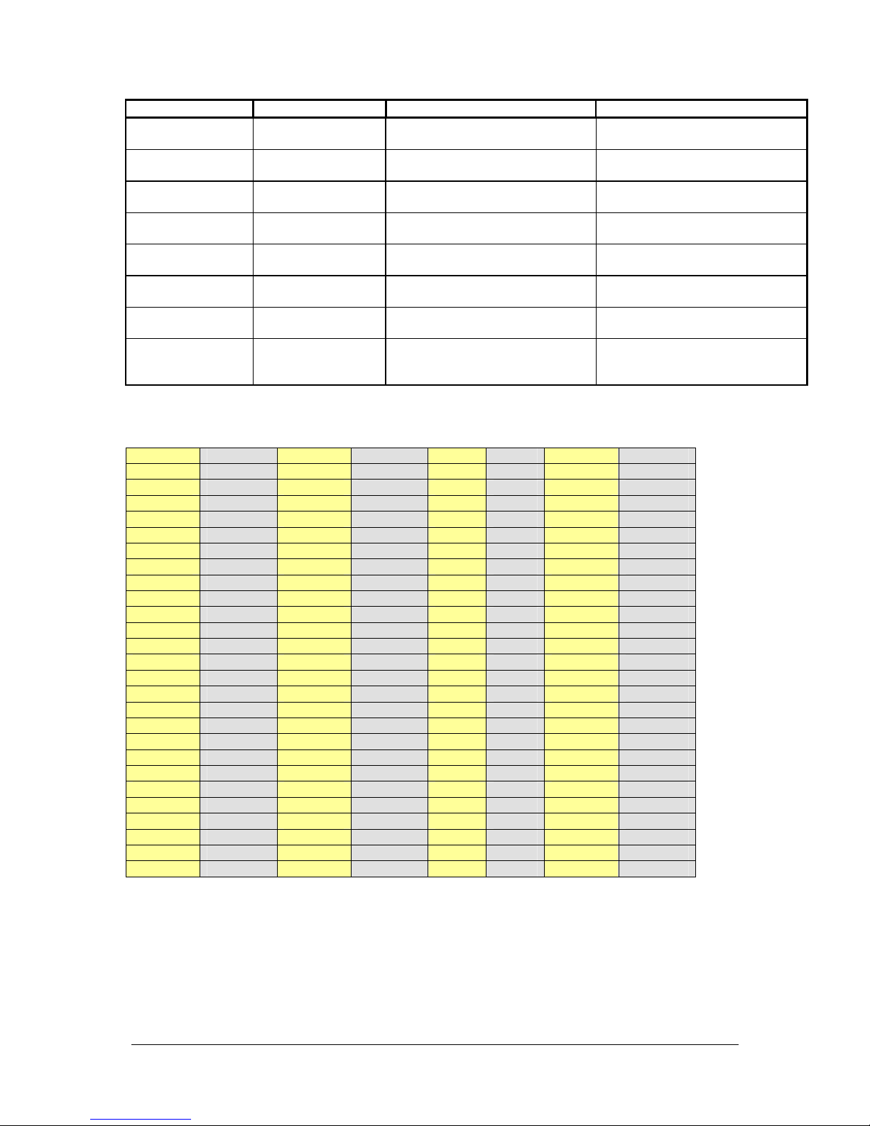
3. Other control
0x55
U 0x75
u
Function Command Description Acknowledge (if enabled)
Select RS-232
acknowledge
Image Auto
Adjust#
Command
availability
Color Auto Adjust# 0xc5 Start auto-calibration of gain of
Query BIOS
0xc1, “0” | “1” Disable/enable command
acknowledge.
“0” – acknowledge disabled.
“1” – acknowledge enabled.
0xc3 Start auto-setup of current mode. “0” – fail.
“1” – successful.
0xc4, n Check whether a command is
available.
“0” – not available.
“1” – available.
“0” – fail.
the RGB amplifier.
“1” – successful.
0xcb, “0” Read BIOS version “nnnn” = BIOS ver. “nn.nn”
version
Query PCBA
number
Factory Reset 0xce Reset all parameters to factory
0xcb, “1” Read PCBA number “nnnn” = PCBA number
ALR-1400v2=”41758”
“1” – successful.
default value
Soft Power On/Off 0xc8,
“0” | “1” |
“?”
Soft power
off/on
query
“0” – Turn off the LCD panel
power output
“1” – Turn on the unit
# - Function in VGA mode only
Hex to ASCII conversion table
Hex ASCII Hex ASCII Hex ASCII Hex ASCII
0x30 0 0x41 A 0x61 a 0x2B +
0x31 1 0x42 B 0x62 b 0x2D -
0x32 2 0x43 C 0x63 c 0x3F ?
0x33 3 0x44 D 0x64 d
0x34 4 0x45 E 0x65 e
0x35 5 0x46 F 0x66 f
0x36 6 0x47 G 0x67 g
0x37 7 0x48 H 0x68 h
0x38 8 0x49 I 0x69 i
0x39 9 0x4A J 0x6A j
0x4B K 0x6B k
0x4C L 0x6C l
0x4D M 0x6D m
0x4E N 0x6E n
0x4F O 0x6F o
0x50 P 0x70 p
0x51 Q 0x71 q
0x52 R 0x72 r
0x53 S 0x73 s
0x54 T 0x74 t
0x56 V 0x76 v
0x57 W 0x77 w
0x58 X 0x78 x
0x59 Y 0x79 y
0x5A Z 0x7A z
Specifications subject to change without notice
© Digital View Ltd – Doc Ver 2.00: 15 November, 2017 Page
29 of 35
Page 30
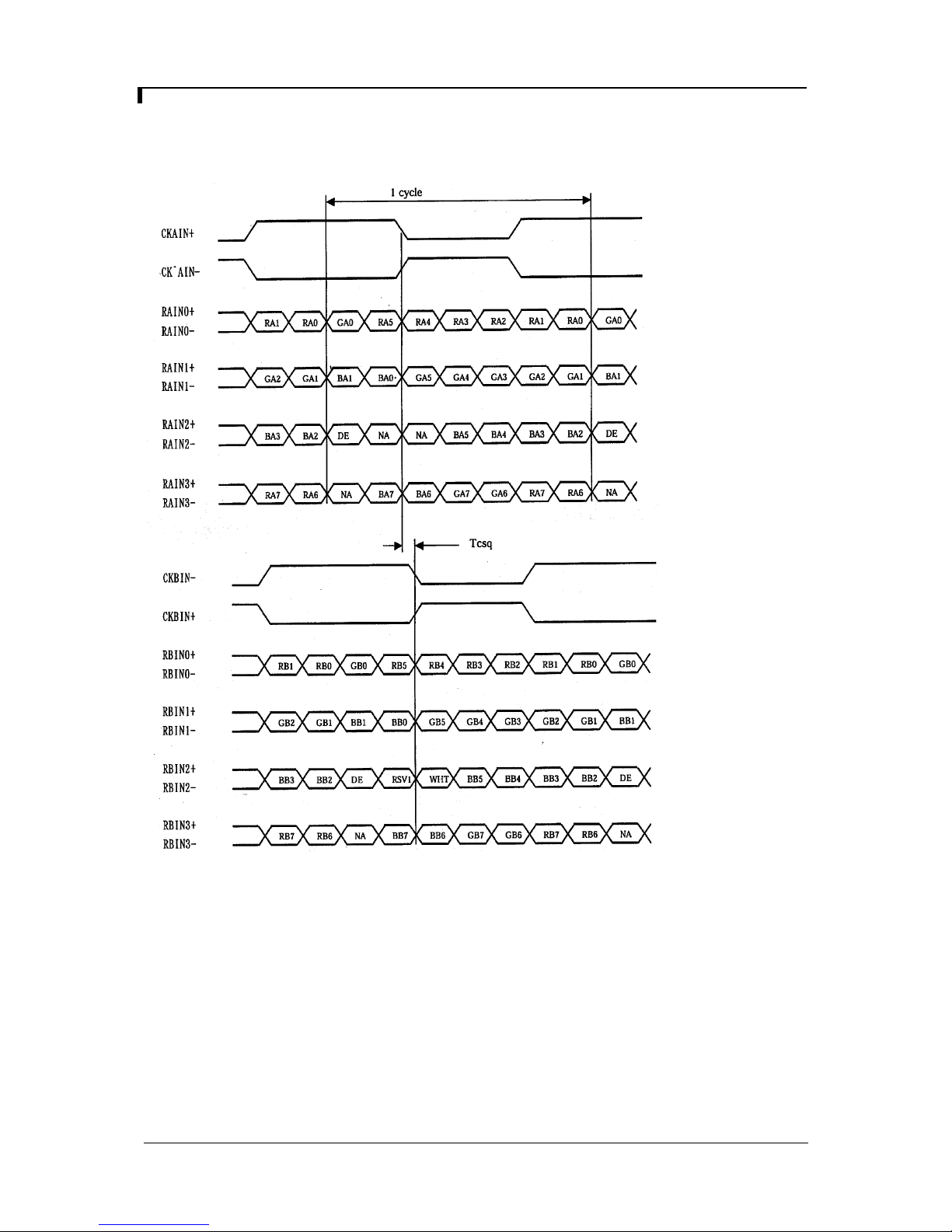
Appendix III – Mapping definition
• Definition of Mapping A :
Specifications subject to change without notice
© Digital View Ltd – Doc Ver 2.00: 15 November, 2017 Page
30 of 35
Page 31
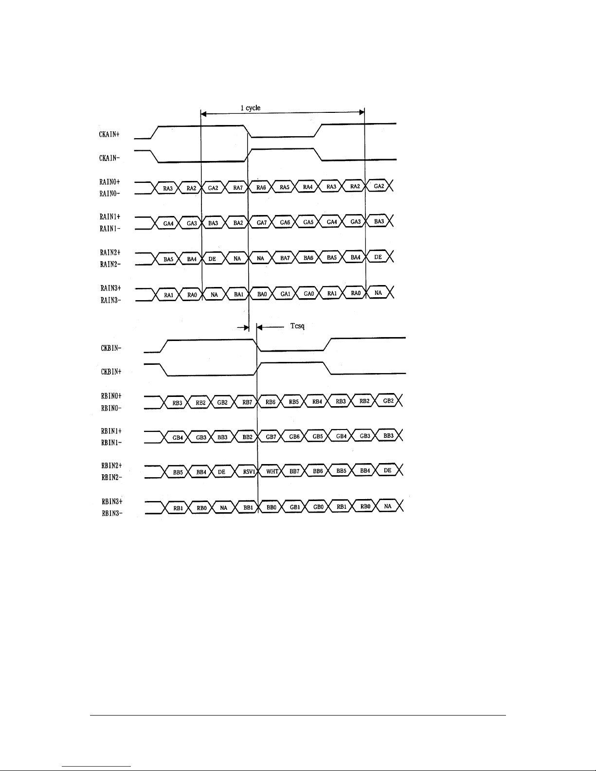
• Definition of Mapping B :
Specifications subject to change without notice
© Digital View Ltd – Doc Ver 2.00: 15 November, 2017 Page
31 of 35
Page 32
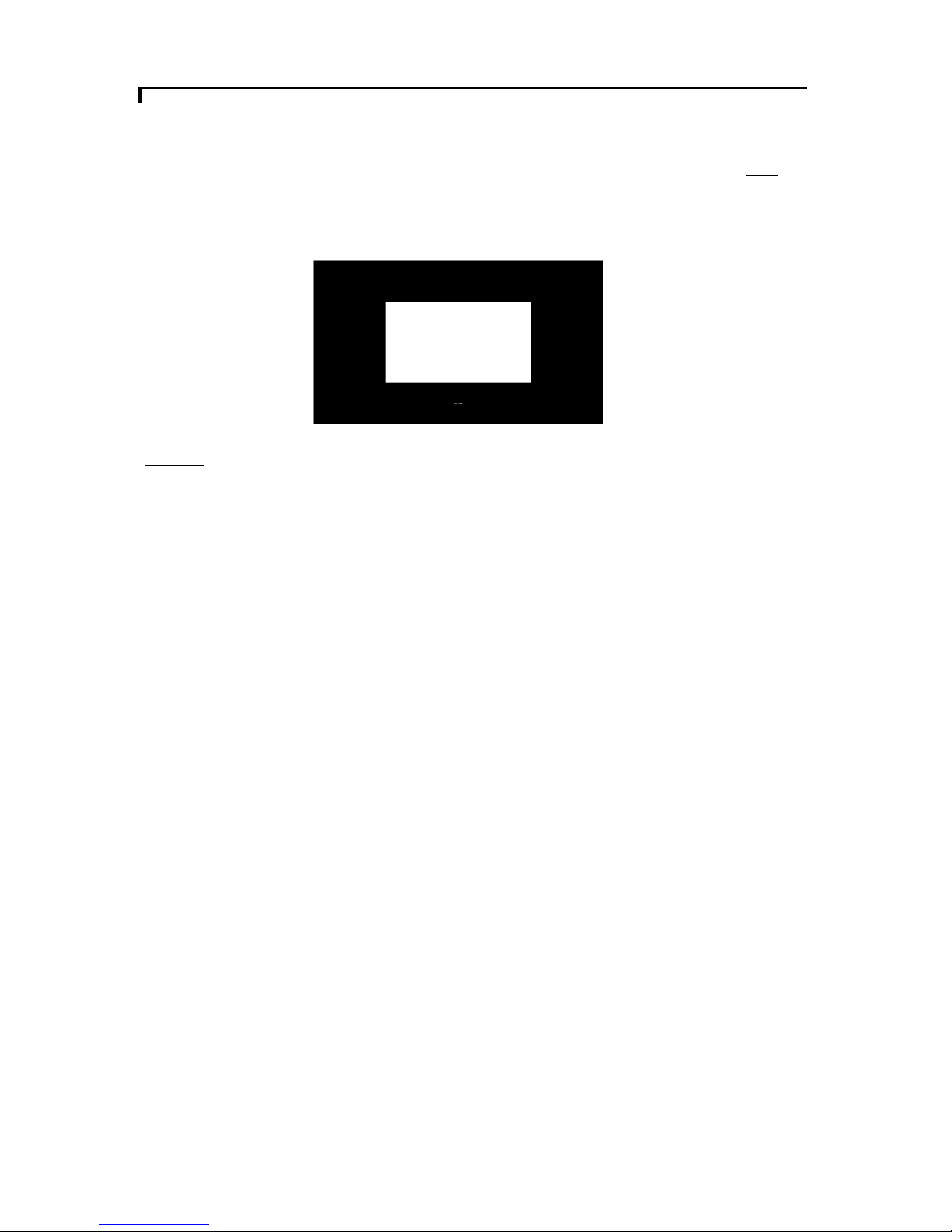
Appendix IV – Color Auto Adjust
The Color Auto Adjust function is supported in the VGA mode only and is designed to
calibrate the controller to the incoming video signal. In order to calibrate correctly, the display must be
displaying an image containing both black and white data (see illustration below) when the function is
used. The internal processor of the video controller chip will then execute a process to adjust the
relative values of the RGB signals to achieve the best performance. The parameters of the corrected
RGB values are then stored in the controller and are unaffected by the Reset Factory Defaults
function.
Warning - If the Color Auto Adjust is executed without an appropriate image being displayed, then the
process will set incorrect values and the display colors will be distorted. If this occurs, then it can
either be corrected by performing the process correctly or if this is not possible then the Reset Color
Gain function can be used. This function will reset the stored RGB values to a set of approximate
values.
Specifications subject to change without notice
© Digital View Ltd – Doc Ver 2.00: 15 November, 2017 Page
32 of 35
Page 33
WARRANTY
The products are warranted against defects in workmanship and material for a period of three (3) year from the date of
purchase provided no modifications are made to it and it is operated under normal conditions and in compliance with the
instruction manual.
The warranty does not apply to:
• Product that has been installed incorrectly, this specifically includes but is not limited to cases where electrical short
circuit is caused.
• Product that has been altered or repaired except by the manufacturer (or with the manufacturer’s consent).
• Product that has subjected to misuse, accidents, abuse, negligence or unusual stress whether physical or electrical.
• Ordinary wear and tear.
Except for the above express warranties, the manufacturer disclaims all warranties on products furnished hereunder, including
all implied warranties of merchantability and fitness for a particular application or purpose. The stated express warranties are in
lieu of all obligations or liabilities on the part of the manufacturer for damages, including but not limited to special, indirect
consequential damages arising out of or in connection with the use of or performance of the products.
CAUTION
Whilst care has been taken to provide as much detail as possible for use of this product it cannot be relied upon as
an exhaustive source of information. This product is for use by suitably qualified persons who understand the nature
of the work they are doing and are able to take suitable precautions and design and produce a product that is safe
and meets regulatory requirements.
LIMITATION OF LIABILITY
The manufacturer’s liability for damages to customer or others resulting from the use of any product supplied hereunder shall
in no event exceed the purchase price of said product.
TRADEMARKS
The following are trademarks of Digital View Ltd:
• Digital View
• HE-1400v2
Specifications subject to change without notice
© Digital View Ltd – Doc Ver 2.00: 15 November, 2017 Page
33 of 35
Page 34

CONTACT DETAILS
Digital View has offices in Asia, Europe and USA also an internet site:
USA
Digital View Inc.
18440 Technology Drive
Building 130
Morgan Hill,
California, 95037
USA
Tel: (1) 408-782 7773 Fax: (1) 408-782 7883
EUROPE
Digital View Ltd.
The Lake House
Knebworth Park
Herts, SG3 6PY
UK
Tel: +44-(0)20-7631-2150 Fax: Fax: +44-(0)20-7631-2156
ASIA
Digital View Ltd
Unit 705-708, 7/F Texwood Plaza
6 How Ming Street
Kwun Tong
Hong Kong
Tel: (852) 2861 3615 Fax: (852) 2520 2987
WEBSITE
www.digitalview.com
Specifications subject to change without notice
© Digital View Ltd – Doc Ver 2.00: 15 November, 2017 Page
34 of 35
Page 35
Date
Rev No.
Page
Summary
Revision History
15 Nov 2017 2.00 All First Issue version.
Specifications subject to change without notice
© Digital View Ltd – Doc Ver 2.00: 15 November, 2017 Page
35 of 35
 Loading...