

Page 1
TECHNICAL USER'S MANUAL FOR:
PC/104
MSM586SEN/SEV
(optional SN/SV)
Nordstrasse 11/F
CH- 4542 Luterbach
Tel.: ++41 (0)32 681 58 00
Fax: ++41 (0)32 681 58 01
Email: support@digitallogic.com
Homepage:
http://www.digitallogic.com
Page 2
DIGITAL-LOGIC AG MSM586SEN/SEV Manual V1.5E
2
COPYRIGHT 1999- 2004 BY DIGITAL-LOGIC AG
No part of this document may be reproduced, transmitted, transcribed, stored in a retrieval system, in any
form or by any means, electronic, mechanical, optical, manual, or otherwise, without the prior written permission of DIGITAL-LOGIC AG.
The software described herein, together with this document, are furnished under a license agreement and
may be used or copied only in accordance with the terms of that agreement.
ATTENTION:
All information in this manual and about the product are subject to change without prior notice.
REVISION HISTORY:
Prod.-Serialnumber:
From: To:
Product
Version
BIOS
Version
Doc.
Version
Date/Vis:
Modification:
Remarks, News, Attention:
150xxx10000 150xxx1yyyy
V1.1 None 0.01 05.2000 FK Initial version, Development
V2.1 V1.20 V1.2 06.2001 STP Serial product
V2.1 V1.21 V1.3 08.2001 STP Remote, COM’s, jumper, memory
map, etc
V2.1 V1.21 V1.4 09.2001 STP Thermopicture, etc
V2.2 V1.23 V1.4 10.2001 KUF Current, Boottime, BAT-Lifetime
V2.3 V1.26 V1.5 08.2003 KUF
IrDA, Eratas
Kap 5.6.2. J58 always on 1-2
p76 contrast control removed
Kap 8.1. remark for J49/50 position of V2.1
Kap 11.1.3. remoteenabler DSUB-pins
J54 deleted in Kap 7.
V2.4 1.26 1.5A 01.2004 DAR RS485/422 description added
V2.4 1.26 1.5B 04.2004 DAR Int15 / minor corrections
V2.5 1.26 1.5C 08.2004 DAR Bios history corrected, minor correc-
tions
V2.5 1.26 1.5D 08.2004 DAR Bios download, front picture
V2.5 1.26 1.5E 11.2004 DAR LAN interface, RS485
ATTENTION
1. All information in this manual and the product are subject to change without prior notice.
2. Read this manual prior installation of the product.
3. Read the security information carefully prior installtion of the product.
Registration:
http://www.digitallogic.com -> SUPPORT -> embedded products -> register
After registration, you will receive driver & software updates, errata information, customer information and
news from DIGITAL-LOGIC AG products automatically.
Page 3

DIGITAL-LOGIC AG MSM586SEN/SEV Manual V1.5E
3
Table of Contents
1 Preface.............................................................................................................................6
1.1 Trademarks....................................................................................................................... 6
1.2 Disclaimer......................................................................................................................... 6
1.3 Environmental Protection Statement.............................................................................. 6
1.4 Explanation of Symbols................................................................................................... 7
1.5 For Your Safety ................................................................................................................ 9
1.6 Limited Two Year Warranty ........................................................................................... 10
2 Overview........................................................................................................................11
2.1 Standard Features.......................................................................................................... 11
2.2 Unique Features............................................................................................................. 11
2.3 MSM586SEN/SEV block diagram ................................................................................ 12
2.4 Specifications................................................................................................................. 13
2.5 BIOS History................................................................................................................... 16
2.6 This product is “YEAR 2000 CAPABLE” ........................................................ 16
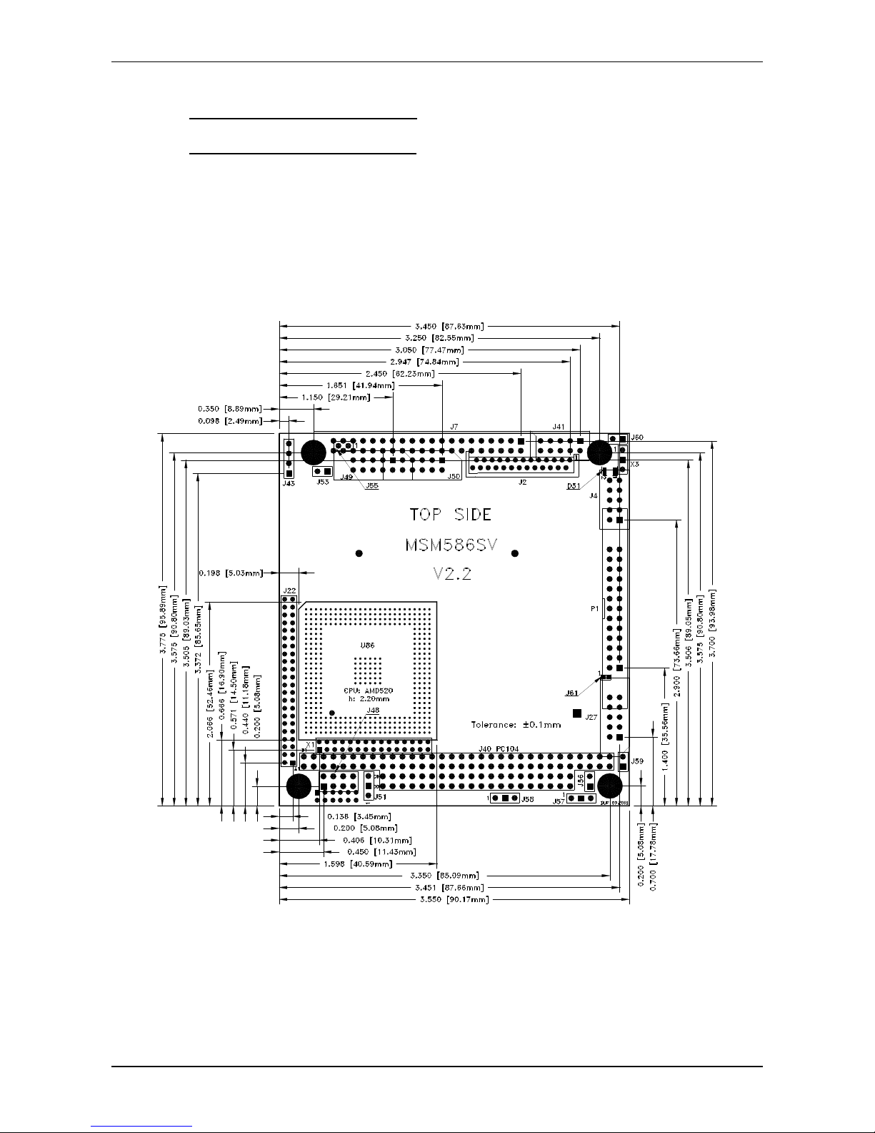
2.7 Mechanical Dimensions................................................................................................. 17
2.7.1 Board version V2.2/2.3/2.4/2.5 .................................................................................................. 17
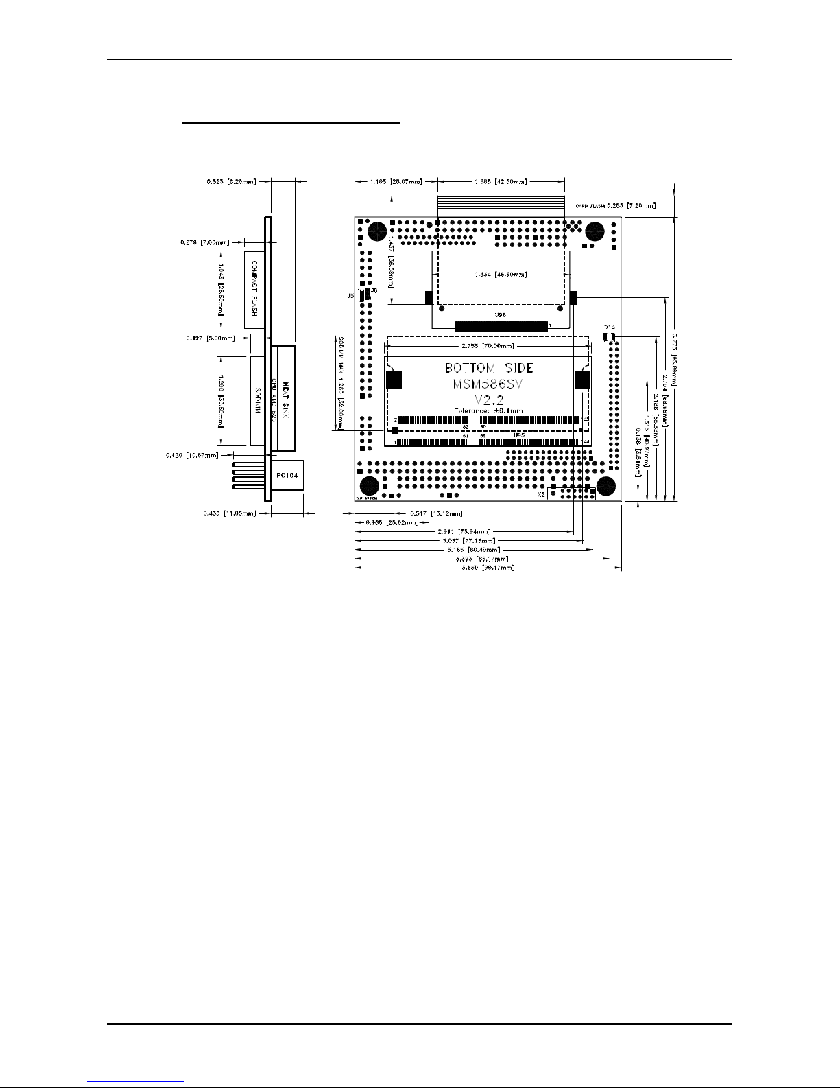
2.7.2 Board version V2.2/2.3/2.4/2.5 .................................................................................................. 18
2.8 Incompatibilities to a standard PC/AT.......................................................................... 19
2.9 Related application notes.............................................................................................. 19
2.10 Ordering codes ........................................................................................................... 19
2.11 Thermoscan ................................................................................................................ 20
2.12 High frequency radiation (to meet EN55022 & EN61000) ......................................... 21
3 PC/104 Bus Signals .....................................................................................................22
3.1 Bus levels ....................................................................................................................... 26
4 Detailed System Description .......................................................................................27
4.1 Power Requirements ..................................................................................................... 27
4.2 CPU, Boards and RAMs................................................................................................. 29
4.2.1 CPUs of this MICROSPACE Product ........................................................................................ 29
4.2.2 Numeric Coprocessor ................................................................................................................ 29
4.2.3 DRAM Memory .......................................................................................................................... 29
4.3 Interface.......................................................................................................................... 30
4.3.1 Keyboard AT compatible and PS/2 Mouse................................................................................ 30
4.3.2 Line Printer Port LPT1 ............................................................................................................... 30
4.3.3 Serial Ports COM1-COM4 ......................................................................................................... 30
4.3.4 Floppy Disk Interface ................................................................................................................. 33
4.3.5 Speaker interface....................................................................................................................... 34
4.3.6 LAN Interface: ............................................................................................................................ 34
4.4 Controllers...................................................................................................................... 35
4.4.1 Interrupt Controllers ................................................................................................................... 35
4.5 Timers and Counters ..................................................................................................... 35
4.5.1 Programmable Timers ............................................................................................................... 35
4.5.2 Internal Battery backed clock (RTC).......................................................................................... 36
4.5.3 External Battery assembling: ..................................................................................................... 36
4.5.4 Watchdog................................................................................................................................... 37
4.6 Boottime ......................................................................................................................... 38
5 BIOS ...............................................................................................................................39
5.1 ROM-BIOS sockets ........................................................................................................ 39
5.2 Standard BIOS ROM ...................................................................................................... 39
5.3 EEPROM Memory for Setup .......................................................................................... 39
5.3.1 BIOS CMOS Setup .................................................................................................................... 40
5.4 CMOS RAM Map............................................................................................................. 40
Page 4

DIGITAL-LOGIC AG MSM586SEN/SEV Manual V1.5E
4
5.5 EEPROM saved CMOS Setup........................................................................................ 46
5.6 CORE / VGA - BIOS download function........................................................................ 47
5.6.1 CORE BIOS download function ................................................................................................. 47
5.6.2 VGA BIOS download function.................................................................................................... 48
5.7 Memory ........................................................................................................................... 49
5.7.1 System Memory Map ................................................................................................................. 49
5.7.2 System I/O map ......................................................................................................................... 49
5.8 BIOS Data Area Definitions ........................................................................................... 64
5.8.1 Compatibility Service Table ....................................................................................................... 70
6 VGA, LCD.......................................................................................................................71
6.1 VGA / LCD controller 69000........................................................................................... 71
6.2 VGA / LCD BIOS for 69000........................................................................................... 71
6.3 Display modes supported ............................................................................................. 72
6.4 VGA/LCD BIOS support................................................................................................. 73
6.5 Memory 69000 CRT/TFT panels ................................................................................... 74
6.6 Memory 69000 color STN-DD panels ........................................................................... 75
6.7 Memory 69000 Mono STN-DD panels .......................................................................... 76
7 Description of the connectors .....................................................................................77
8 Jumper locations on the board....................................................................................90
8.1 Jumpers locations on the MSM586SEN/SEV V2.2/2.3/2.3a/2.4/2.5............................. 91
9 LED criterions: ..............................................................................................................93
10 Cable interface ............................................................................................................94
10.1 The harddisk cable 44pin ........................................................................................... 94
10.2 The COM 1/2/3/4 serial interface cable ...................................................................... 95
10.3 The printer interface cable (P1).................................................................................. 96
10.4 The Micro Floppy interface cable .............................................................................. 97
11 Remote Function.........................................................................................................98
11.1 Remote Features......................................................................................................... 98
11.1.1 The Remote Server REMHOST.EXE ........................................................................................ 98
11.1.2 Remote enabler ......................................................................................................................... 99
11.1.3 Cable Definition (DSUB-9pin-female)........................................................................................ 99
11.1.4 Restrictions .............................................................................................................................. 100
12 Software.....................................................................................................................100
13 100/10 Ethernet LAN ................................................................................................101
13.1 Intel 82559ER Ethernet chip..................................................................................... 101
13.1.1 Installation example for MSDOS Novell 4.11........................................................................... 101
13.1.2 Driver installation WINDOWS 95 ............................................................................................. 102
13.1.3 Driver installation WINDOWS 98SE ........................................................................................ 102
13.1.4 EEPROM update ..................................................................................................................... 102
13.2 Intel 82559 Ethernet chip.......................................................................................... 103
13.2.1 Installation example for MSDOS Novell 4.11........................................................................... 103
13.2.2 Driver installation WINDOWS 95 ............................................................................................. 103
13.2.3 Driver installation WINDOWS 98SE ........................................................................................ 103
13.2.4 EEPROM update ..................................................................................................................... 104
14 Installing the flashdisk DOC2000 ............................................................................105
14.1 Enabling and formatting of the DiskOnChip-module ............................................. 105
14.2 Compact Flash (CF).................................................................................................. 105
15 Special Peripherals, Configuration .........................................................................106
15.1 The special function interface for MICROSPACE ................................................... 106
16 Building a system .....................................................................................................109
16.1 Starting up the system ............................................................................................. 109
Page 5

DIGITAL-LOGIC AG MSM586SEN/SEV Manual V1.5E
5
17 Diagnostics ...............................................................................................................110
17.1 Failures and hints ..................................................................................................... 110
17.1.1 Other, so far not identified problems........................................................................................ 110
17.2 POST-CODE Description.......................................................................................... 111
17.2.1 Boot Loader.............................................................................................................................. 111
17.2.2 Error Beep codes ..................................................................................................................... 111
17.2.3 System BIOS in Shadow RAM................................................................................................. 111
17.2.4 Error Beep codes ..................................................................................................................... 112
18 Assemblings view.....................................................................................................113
18.1 MSM586SV/SN – SEV/SEN V2.3a/2.4/2.5 ................................................................. 113
19 INDEX.........................................................................................................................115
Page 6

DIGITAL-LOGIC AG MSM586SEN/SEV Manual V1.5E
6
1 P
REFACE
This document is for integrators and programmers of systems based on the MICROSPACE-Computer family.
It contains information on hardware requirements, interconnections, and details of how to program the system. The specifications given in this manual were correct at the time of printing; advances mean that some
may have changed in the meantime.
The information contained in this document is, to the best of our knowledge, entirely correct. However,
DIGITAL-LOGIC AG, cannot accept liability for any inaccuracies or the consequences thereof, of for any liability arising from the use or application of any circuit, product decribed herein, as seen fit by DIGITALLOGIC AG without further notice.
1.1 Trademarks
Digtial-Logic , Digital-Logic-Logo, MICROSPACE, smartModule are registered trademarks owned worldwide
by Digital-Logic AG Luterbach (Switzerland). In addition, this document may include names, company logos,
and trademarks which are registered trademarks and are therefore proprietary to their respective owners.
1.2 Disclaimer
DIGITAL-LOGIC AG makes no representations or warranties with respect to the contents of this manual and
specifically disclaims any implied warranty of merchantability or fitness for any particular purpose. DIGITALLOGIC AG shall under no circumstances be liable for incidental or consequential damages or related expenses resulting from the use of this product, even if it has been notified of the possibility of such damage.
DIGITAL-LOGIC AG reserves the right to revise this publication from time to time without obligation to notify
any person of such revisions
1.3 Environmental Protection Statement
This product has been manufactured to satisfy environmental protection requirements where possible. Many
of the components used (structural parts, printed circuit baords, connectors, batteries, etc.) are capable of
being recycled.
Final disposition of this product after its service life must be accomplished in accordance with applicable
country, state, or local laws or regulations.
Page 7
DIGITAL-LOGIC AG MSM586SEN/SEV Manual V1.5E
7
1.4 Explanation of Symbols
CE Conformity
This symbol indicates that the product described in this manual is in compliance with all applied CE
standards. Please refer also to the section “Applied Standards” in this manual.
Caution, Electric Shock!
This symbol and title warn of hazards due to electrical shocks (> 60V) when touching products or
parts of them. Failure to observe the precautions indicated and/or prescribed by the law may endanger your life/health and/or result in damage to your material. Please refer also to the section
“High Voltage Safety Instructions” on the following page.
Warning, ESD Sensitive Device!
This symbol and title inform that electronic boards and their components are sensitive to static electricity. Therefore, care must be taken during all handling operations and inspections of this product, in order to ensure product integrity at all times. Please read also the section “Special Handling and Unpacking Instructions” on the following page.
Warning!
This symbol and title emphasize points which, if not fully understood and taken into consideration
by the reader, may endanger your health and/or result in damage to your material.
Note...
This symbol and title emphasize aspects the reader should read through carefully for his or her
own advantage.
Page 8

DIGITAL-LOGIC AG MSM586SEN/SEV Manual V1.5E
8
This symbol and title warn of general hazards from mechanical, electrical, chemical failure. This may
Endager your life/health and/or result in damage to your material.
Page 9
DIGITAL-LOGIC AG MSM586SEN/SEV Manual V1.5E
9
1.5 For Your Safety
Your new Digital-Logic product was developed and tested carefully to provide all features
necessary to ensure its compliance with electrical safety requirements. It was also designed for a long fault-free life. However, the life expectancy of your product can be drastically reduced by improper treatment during unpacking and installation. Therefore, in the
interest of your own safety and of the correct operation of your new Digital-Logic product,
you are requested to conform with the following guidelines.
Warning!
All operations on this device must be carried out by sufficiently skilled personnel only.
Caution, Electric Shock!
Before installing your new Digital-Logic product, always ensure that your mains power is switched
off. This applies also to the installation of piggybacks or peripherials. Serious electrical shock hazards can exist during all installation, repair and maintenance operations with this product. Therefore, always unplug the power cable and any other cables which provide external voltages before
performing work.
ESD Sensitive Device!
Electronic boards and their components are sensitive to static electricity. Therefore, care must be
taken during all handling operations and inspections of this product, in order to ensure product integrity at all times.
Page 10

DIGITAL-LOGIC AG MSM586SEN/SEV Manual V1.5E
10
1.6 Limited Two Year Warranty
DIGITAL-LOGIC AG warrants the hardware and software products it manufactures and produces to be free
from defects in materials and workmanship for one year following the date of shipment from DIGITAL-LOGIC
AG, Switzerland. This warranty is limited to the original purchaser of product and is not transferable.
During the one year warranty period, DIGITAL-LOGIC AG will repair or replace, at its discretion, any defective product or part at no additional charge, provided that the product is returned, shipping prepaid, to
DIGITAL-LOGIC AG. All replaced parts and products become property of DIGITAL-LOGIC AG.
Before returning any product for repair, customers are required to contact the company or their distributor.
This limited warranty does not extend to any product which has been damaged as a result of accident, misuse, abuse (such as use of incorrect input voltages, wrong cabling, wrong polarity, improper or insufficient
ventilation, failure to follow the operating instructions that are provided by DIGITAL-LOGIC AG or other contingencies beyond the control of DIGITAL-LOGIC AG), wrong connection, wrong information or as a result of
service or modification by anyone other than DIGITAL-LOGIC AG. Neither, if the user has not enough
knowledge of these technologies or has not consulted the product manual or the technical support of
DIGITAL-LOGIC AG and therefore the product has been damaged.
Except, as expressly set forth above, no other warranties are expressed or implied, including, but not limited
to, any implied warranty of merchantability and fitness for a particular purpose, and DIGITAL-LOGIC AG expressly disclaims all warranties not stated herein. Under no circumstances will DIGITAL-LOGIC AG be liable
to the purchaser or any user for any damage, including any incidental or consequential damage, expenses,
lost profits, lost savings, or other damages arising out of the use or inability to use the product.
Page 11

DIGITAL-LOGIC AG MSM586SEN/SEV Manual V1.5E
11
2 O
VERVIEW
2.1 Standard Features
The MICROSPACE PC/104 is a miniaturized modular device incorporating the major elements of a PC/AT
compatible computer.
It includes standard PC/AT compatible elements, such as:
- Powerful ELAN520 133MHz
- BIOS ROM
- SODIMM 16 to 128 MBytes 70ns (32bit device, no ECC supported)
- Timers
- DMA
- Real-time clock with CMOS-RAM and battery buffer
- LPT1 parallel port
- COM1, COM2, COM3, COM4 serial port
- Speaker interface
- AT-keyboard interface or PS/2-keyboard interface
- PS/2 mouse interface
- Floppy disk interface
- AT-IDE harddisk interface
- VGA/LCD video interface
- PC/104 embedded BUS
2.2 Unique Features
The MICROSPACE includes all standard PC/AT functions plus unique DIGITAL-LOGIC AG enhancements,
such as:
- Single 5 volt supply
- LAN Ethernet 82559ER
- DOC2000
- Compact card. typ 1
- Watchdog
- Power-fail
- EEPROM for setup and configuration
- Core- and VGA BIOS downloadable
- JTAG for debugging with CADUL KIT
- (NO Power management functions yet)
- UL approved parts
Page 12
DIGITAL-LOGIC AG MSM586SEN/SEV Manual V1.5E
12
DRAM
BUS
2.3 MSM586SEN/SEV block diagram
ELAN520
CPU
SODIMM
up to 128 Mbyte
EIDE
&
CF
LCD/VGA
Controller 69000
PCI-BUS
LCD
CRT
BIOS
256kByte
Super I/O
37B787
PC/10
4
Bus
Ethernet
LAN
INTEL 82559ER
ISA-BUS
MAX2ll
FD
LPT1
MAX2ll
COM3 COM4
JTAG Port
RTC
LiBAT
EEPROM
2kByte
Watchdog
KB Mouse
100/10BASE-T
VRAM
2 MB
MAX2ll
MAX2ll
COM1 COM2
IrDA
DOC2000
Page 13
DIGITAL-LOGIC AG MSM586SEN/SEV Manual V1.5E
13
2.4 Specifications
CPU:
Specification
CPU
AMD ELAN520 – 133MHz
Compatibility: 8086 – Pentium
1. Level Cache: 16k data and 16k code
2. Level Cache: None
Socket: BGA
Clock 133MHz
FSB 33MHz
Powermanagement None
FPU: Integrated
Chipset:
Specification
Nordbridge AMD ELAN520
Southbridge AMD ELAN520
LAN 82C559 INTEL
Audio Not on board
Firewire IEEE1394 Not on board
Video CT69000 (2Mbyte)
Framegrabber/TV-Input Not on board
Memory
Specification
Main Memory SDRAM, 32Bit, up to 128Mbyte in two SODIMM144 socket
Flash-BIOS 256kByte Flash
Setup EEPROM 2kByte for CMOS-backup in batterless applications
Flash-VideoBIOS: Serial-Flash
Video RAM Separate 2Mbyte
Video controller
Specification
Controller CT69000
Videomemory 4Mbyte
Channel 1 CRT VGA up to 1248 x 1024 pixels
Channel 2 TFT
Bootup-Resolution 640 x 480 / 800 x 600 / 1024 x 768 VGA bios depending
2D-Grafic Integrated accelerator
3D-Grafic Not available
Direct-X Version Not available
PnP Not available
Page 14
DIGITAL-LOGIC AG MSM586SEN/SEV Manual V1.5E
14
External Interface
Specification
Videointerfaces CRT1, LCD for TFT and STN
USB V1.1 Not available
LPT1: Internal
COM1: RS232
COM2: RS232
COM3: RS232
COM4: RS232
Keyboard: PS/2
Mouse: PS/2
Floppy: 26pin FCC Interface for TEAC Minifloppy
Harddisk: 1 channel 44pin RM2.0mm ATAIDE-cable
Speaker: 0.1Watt Speaker
Powersupply:
Input: Nom. 5V Tolerance +/- 3%
Protection: Not integrated, EMI filtered must be added external
Spec.
Power Consumption
Specification
At 5V Typical 1.5 Amp.
Standby Not available
Poweroff 0mA
Physical Characteristics
Specification
PC/104
Dimensions: Length: 91mm
Depth: 96mm
Height: 25mm
Weight: 170gr
Operating Environment
Specification
Relative Humidity: 5 - 90% non condensing
IEC68-2-30 at -20° to +50°C operating
Vibration operating: IEC68-2-6 10-50Hz, 0.075mm and 55-500Hz, 1.0G
Vibration nonoperating: IEC68-2-6 10-50Hz, 0.15mm and 55-500Hz, 2.0G
Shock operating: IEC68-2-27 10G, 11ms ½ sine
Shock nonoperating: IEC68-2-27 50G, 11ms, ½ sine
Altitude IEC68-2-13 4571meter operating
Temperature operating IEC68-2-1,2,14: Standard -20°C to +60°C
Extended Temp. option MIL-810-501/502 Extended temperatur -40°C to +85°C
Temperature storage IEC68-2-1,2,14: -65°C to +125°C *)
*) The backupbattery is limited on –40°C to +85°C operating and storage temperature !
Page 15
DIGITAL-LOGIC AG MSM586SEN/SEV Manual V1.5E
15
EMI / EMC Tests
Specification
If all signals are externaly filtered and assembled into a closed metalic case !
EMC emission EN61000-6-2:2001
Conducted disturbance EN55022 Class B
Radiated disturbance EN55022 Class B
EMC immunity EN61000-6-2
Electrostatic discharge (ESD) EN61000-4-2
Voltage = 4kV contact / 8kV air
Criteria A
Radiated RF-Field EN61000-4-3
Level = 10V/m
Criteria A
Electrical fast transients (Burst) EN61000-4-4
Grade 2: DC-Powerlines = 1000V (5/50ns)
Grade 2: AC-Powerlines = 2000V (5/50ns)
Grade 2: Signallines = 500V (5/50ns)
Criteria B
Surge EN61000-4-5
Grade 2: DC-Powerlines = 1kV, (1.2/50us)
Grade 2: AC-Powerlines = 2kV, (1.2/50us)
Criteria B
Conducted disturbances EN61000-4-6
Voltage = 10V coupled by case
Criteria A
Security:
e1: Not planed
UL Not planed
ETS 301 Not planed
CE/SEV Yes
Safety AR385-16
Any information is subject to change without notice.
Page 16

DIGITAL-LOGIC AG MSM586SEN/SEV Manual V1.5E
16
2.5 BIOS History
Version: Date: Status: Modifications:
V1.00 Mai.2000 Development Test Initial prototyp BIOS
V1.11 06.2001 Development Test Initial standard BIOS
V1.20 06.2001 Beta Standard BIOS for boardversions >2.0
V1.21 08.2001 Beta DOC2000 support, IRQ15 enabled, FDD B off,
V1.22 09.2001 Released IN10 disabled, LPT en/disable, date 1.1.2000 battery less
V1.23 10.2001 Released INT10 in E- segment
V1.25 09.2002 Released INT15, HD autodetect, CD-Rom support, default settings, no
F1 stop if the floppy fails during boot up
V1.26 08.2003 Released IrDA, Download BIOS, FFS, DOC2000 >92MB working now
2.6 This product is “YEAR 2000 CAPABLE”
This DIGITAL-LOGIC product is “YEAR 2000 CAPABLE”. This means, that upon installation, it accurately
stores, displays, processes, provides and/or receives date data from, into, and between 1999 and 2000, and
the 20. and 21. centuries, including leap year calculations, provided that all other technology used in combination with said product properly exchanges date data with it. DIGITAL-LOGIC makes no representation
about individual components within the product should be used independently from the product as a whole.
You should understand that DIGITAL-LOGIC’s statement that an DIGITAL-LOGIC product is “YEAR 2000
CAPABLE” means only that DIGITAL-LOGIC has verified that the product as a whole meet this definition
when tested as a stand-alone product in a test lab, but dies not mean that DIGITAL-LOGIC has verified that
the product is “YEAR 2000 CAPABLE” as used in your particular situation or configuration. DIGITAL-LOGIC
makes no representation about individual components, including software, within the product should they be
used independently from the product as a whole.
DIGITAL-LOGIC customers use DIGITAL-LOGIC products in countless different configurations and in conjunction with many other components ans systems, and DIGITAL-LOGIC has no way to test wheter all those
configurations and systems will properly handle the transition to the year 2000. DIGITAL-LOGIC encourages
its customers and others to test whether their own computer systems and products will properly handle the
transition to the year 2000.
The only proper method of accessing the date in systems is indirectly from the Real-Time-Clock via the
BIOS. The BIOS in DIGITAL-LOGIC computerboards contain a century checking and maintenance feature
the checks the laest two significant digits of the year stored in the RTC during each BIOS request (INT 1A) to
read the date and, if less than ‘80’ (i.e. 1980 is the first year supported by the PC), updates the century byte
to ‘20’. This feature enables operating systems and applications using BIOS date/time services to reliably
manipulate the year as a four-digit value.
Page 17
DIGITAL-LOGIC AG MSM586SEN/SEV Manual V1.5E
17
2.7 Mechanical Dimensions
2.7.1 Board version V2.2/2.3/2.4/2.5
Page 18
DIGITAL-LOGIC AG MSM586SEN/SEV Manual V1.5E
18
2.7.2 Board version V2.2/2.3/2.4/2.5
Page 19
DIGITAL-LOGIC AG MSM586SEN/SEV Manual V1.5E
19
2.8 Incompatibilities to a standard PC/AT
A. Do not use internal COM1/2 of the ELAN520 in the FIFO-Mode. AMD Errata
Some bits are lost in certain configurations of FIFO-Mode an in extended temperature ranges.
Solution: Use the COM3/4 for FIFO Mode. Use a None-FIFO-Driver !
B. PRETEC Cflash with the Toshiba controller (ACT...) are not working, with
the HITACHI Controller ( ACH...) are aorking fine. A bug fixed by PRETEC.
C. LINUX need a BIOS without INT15 service, otherwise the DRAM-Capacity is not well reported.
Last observation was with BIOS V1.24.
2.9 Related application notes
# Description
84 Power consumption on Pentium / any other boards with
attached drives (HDD, CD)
96 MSM586SEN/SEV upgrades on V1.2
Application Notes are availble at http://www.digitallogic.com -> Support, or on any Application CD from
DIGITAL-LOGIC.
2.10 Ordering codes
To get the actual status of the partnumbers, customers are advised to ask for them
via our sales department or distributors.
Page 20
DIGITAL-LOGIC AG MSM586SEN/SEV Manual V1.5E
20
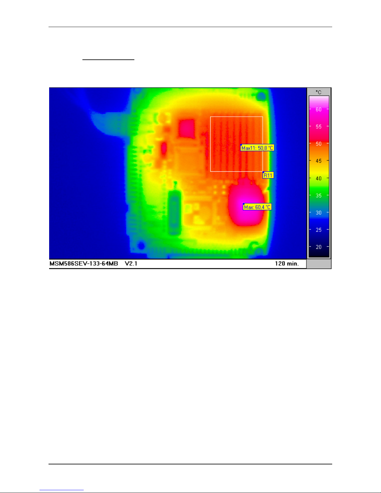
2.11 Thermoscan
With standard cooler:
Page 21

DIGITAL-LOGIC AG MSM586SEN/SEV Manual V1.5E
21
2.12 High frequency radiation (to meet EN55022 & EN61000)
Since the PC/104 CPU modules are very high integrated embedded computers, no peripheral lines are protected against the radiation of high frequency spectrum. To meet a typical EN55022 requirement, all peripherals, they are going outside of the computer case, must be filtered externaly.
Typical signals, they must be filtered:
Keyboard: KBCLK, KBDATA, VCC
Mouse: MSCLK, MSDATA, VCC
COM1/2/3/4: All serial signals must be filtered
LPT: All parallel signals must be filtered
CRT: red,blue,green, hsynch, vsynch must be filtered
Typical signals, they must not be filtered, since they are internaly used:
IDE: connected to the harddisk
Floppy: connected to the floppy
LCD: connected to the internal LCD
1. For peripheral cables:
Use for all DSUB connector a filtered version. Select carefully the filter specifications.
Place the filtered DSUB connector directly frontside and be shure that the shielding makes
a good contact with the case.
9pin DSUB connector from AMPHENOL: FCC17E09P 820pF
25pin DSUB connector from AMPHENOL: FCC17B25P 820pF
2. For stackthrough applications:
Place on each peripheral signal line, they are going outside, a serial inductivity and
after the inductivity a capacitor of 100pF to 1000pF to ground.
In this case, no filtered connectors are needed. Place the filter directly under or
behind the onboard connector.
Serial Inductivity: TDK HF50ACB321611-T 100Mhz, 500mA, 1206 Case
Ground capacitor: Ceramic Capacitor with 1000pF
Power supply:
Use a currentcompensated dualinductor on the 5V supply
SIEMENS B82721-K2362-N1 with 3.6A , 0.4mH
Page 22

DIGITAL-LOGIC AG MSM586SEN/SEV Manual V1.5E
22
3 PC/104 B
US SIGNALS
Please note, that may not all of the signals are available on this board
(check chapter “Description of the connectors”)
AEN, output
Address Enable is used to degate the microprocessor and other devices from the I/O channel to allow DMA
transfers to take place. low = CPU Cycle , high = DMA Cycle
BALE, output
Address Latch Enable is provided by the bus controller and is used on the system board to latch valid addresses and memory decodes from the microprocessor. This signal is used so that devices on the bus can
latch LA17..23. The SA0..19 address lines latched internally according to this signal. BALE is forced high
during DMA cycles.
/DACK[0..3, 5..7], output
DMA Acknowledge 0 to 3 and 5 to 7 are used to acknowledge DMA requests (DRQO through DRQ7). They
are active low. This signal indicates that the DMA operation can begin.
Not available on ELAN520 (DACK5...7)
DRQ[0..3, 5..7], input
DMA Requests 0 through 3 and 5 through 7 are asynchronous channel requests used by peripheral devices
and the I/O channel microprocessors to gain DMA service (or control of the system). A request is generated
by bringing a DRQ line to an active level. A DRQ line must be held high until the corresponding DMA Request Acknowledge (DACK/) line goes active. DRQO through DRQ3 will perform 8-Bit DMA transfers; DRQ57 are used for 16 accesses.
Not available on ELAN520 (DRQ5...7)
/IOCHCK, input
IOCHCK/ provides the system board with parity (error) information about memory or devices on the I/O
channel. low = parity error, high = normal operation
IOCHRDY, input
I/O Channel Ready is pulled low (not ready) by a memory or I/O device to lengthen I/O or memory cycles.
Any slow device using this line should drive it low immediately upon detecting its valid address and a Read
or Write command. Machine cycles are extended by an integral number of one clock cycle (67 nanoseconds). This signal should be held in the range of 125-15600nS. low = wait, high = normal operation
/IOCS16, input
I/O 16 Bit Chip Select signals the system board that the present data transfer is a 16-Bit, 1 wait-state, I/0 cycle. It is derived from an address decode. /IOCS16 is active low and should be driven with an open collector
(300 ohm pull-up) or tri-state driver capable of sinking 20mA. The signal is driven based only on SA15-SAO
(not /IOR or /IOW) when AEN is not asserted. In the 8 Bit I/O transfer, the default transfers a 4 wait-state cycle.
/IOR, input/output
I/O Read instructs an I/O device to drive its data onto the data bus. It may be driven by the system microprocessor or DMA controller, or by a microprocessor or DMA controller resident on the I/O channel. This signal is active low.
Page 23

DIGITAL-LOGIC AG MSM586SEN/SEV Manual V1.5E
23
/IOW, input/output
I/O Write instructs an I/O device to read the data on the data bus. It may be driven by any microprocessor or
DMA controller in the system. This signal is active low.
IRQ[ 3 - 7, 9 - 12, 14, 15], input
These signals are used to tell the microprocessor that an I/O device needs attention. An interrupt request is
generated when an IRQ line is raised from low to high. The line must be held high until the microprocessor
acknowledges the interrupt request.
/Master, input
This signal is used with a DRQ line to gain control of the system. A processor or DMA controller on the I/0
channel may issue a DRQ to a DMA channel in cascade mode and receive a /DACK.
Not available on ELAN520
/MEMCS16, input
MEMCS16 Chip Select signals the system board if the present data transfer is a 1 wait-state, 16-Bit, memory
cycle. It must be derived from the decode of LA17 through LA23. /MEMCS16 should be driven with an open
collector (300 ohm pull-up) or tri-state driver capable of sinking 20mA.
/MEMR input/output
These signals instruct the memory devices to drive data onto the data bus. /MEMR is active on all memory
read cycles. /MEMR may be driven by any microprocessor or DMA controller in the system. When a microprocessor on the I/0 channel wishes to drive /MEMR, it must have the address lines valid on the bus for one
system clock period before driving /MEMR active. These signals are active low.
/MEMW, input/output
These signals instruct the memory devices to store the data present on the data bus. /MEMW is active in all
memory read cycles. /MEMW may be driven by any microprocessor or DMA controller in the system. When a
microprocessor on the I/O channel wishes to drive /MEMW, it must have the address lines valid on the bus
for one system clock period before driving /MEMW active. Both signals are active low.
OSC, output
Oscillator (OSC) is a high-speed clock with a 70 nanosecond period (14.31818 MHz). This signal is not synchronous with the system clock. It has a 50% duty cycle. OSC starts 100µs after reset is inactive.
RESETDRV, output
Reset Drive is used to reset or initiate system logic at power-up time or during a low line-voltage outage. This
signal is active high. When the signal is active all adapters should turn off or tri-state all drivers connected to
the I/O channel. This signal is driven by the permanent Master.
/REFRESH, input/output
These signals are used to indicate a refresh cycle and can be driven by a microprocessor on the I/0 channel.
These signals are active low.
ELAN520 pullup this signal with 1k
ΩΩΩΩ
Page 24

DIGITAL-LOGIC AG MSM586SEN/SEV Manual V1.5E
24
SAO-SA19, LA17 - LA23 input/output
Address bits 0 through 19 are used to address memory and I/0 devices within the system. These 20 address
lines, allow access of up to 1MBytes of memory. SAO through SA19 are gated on the system bus when
BALE is high and are latched on the falling edge of BALE. LA17 to LA23 are not latched and addresses the
full 16 MBytes range. These signals are generated by the microprocessors or DMA controllers. They may
also be driven by other microprocessor or DMA controllers that reside on the I/0 channel. The SA17-SA23
are always LA17-LA23 address timings for use with the MSCS16 signal. This is advanced AT96 design. The
timing is selectable with jumpers LAxx or SAxx.
/SBHE, input/output
Bus High Enable (system) indicates a transfer of data on the upper byte of the data bus, XD8 through XD15.
Sixteen-Bit devices use /SBHE to condition data-bus buffers tied to XD8 through XD15.
SD[O..15], input/output
These signals provide bus bits 0 through 15 for the microprocessor, memory, and I/0 devices. DO is the
least-significant Bit and D15 is the most significant Bit. All 8-Bit devices on the I/O channel should use DO
through D7 for communications to the microprocessor. The 16-Bit devices will use DO through D15. To support 8-Bit device, the data on D8 through D15 will be gated to DO through D7 during 8-Bit transfers to these
devices; 16-Bit microprocessor transfers to 8-Bit devices will be converted to two 8-Bit transfers.
/SMEMR input/output
These signals instruct the memory devices to drive data onto the data bus for the first MByte. /SMEMR is
active on all memory read cycles. /SMEMR may be driven by any microprocessor or DMA controller in the
system. When a microprocessor on the I/0 channel wishes to drive /SMEMR, it must have the address lines
valid on the bus for one system clock period before driving /SMEMR active. The signal is active low.
/SMEMW, input/output
These signals instruct the memory devices to store the data present on the data bus for the first MByte.
/SMEMW is active in all memory read cycles. /SMEMW may be driven by any microprocessor or DMA controller in the system. When a microprocessor on the I/O channel wishes to drive /SMEMW, it must have the
address lines valid on the bus for one system clock period before driving /SMEMW active. Both signals are
active low.
SYSCLK, output
This is a 8.25 MHz system clock. It is a synchronous microprocessor cycle clock with a cycle time of 167
nanoseconds. The clock has a 66% duty cycle. This signal should only be used for synchronization.
Available on ELAN520, since boardversion V2.2
TC output
Terminal Count provides a pulse when the terminal count for any DMA channel is reached. The TC completes a DMA-Transfer. This signal is expected by the onboard floppy disk controller. Do not use this signal,
because it is internally connected to the floppy controller.
/0WS, input
The Zero Wait State (/0WS) signal tells the microprocessor that it can complete the present bus cycle without
inserting any additional wait cycles. In order to run a memory cycle to a 16-Bit device without wait cycles,
/0WS is derived from an address decode gated with a Read or Write command. In order to run a memory
cycle to an 8-Bit device with a minimum of one-wait states, /0WS should be driven active one system clock
after the Read or Write command is active, gated with the address decode for the device. Memory Read and
Write commands to an 8-Bit device are active on the falling edge of the system clock. /OWS is active low
and should be driven with an open collector or tri-state driver capable of sinking 20mA.
Not available on ELAN520
Page 25

DIGITAL-LOGIC AG MSM586SEN/SEV Manual V1.5E
25
12V +/- 5%
used only for the flatpanel supply.
GROUND = 0V
used for the entire system.
VCC, +5V +/- 0.25V
for logic and harddisk/floppy supply.
For further Informations about PC/104 and PC/104plus, please refer to the PC/104 specification
manual which is available on the internet. http://www.digitallogic.com (manuals)
Page 26
DIGITAL-LOGIC AG MSM586SEN/SEV Manual V1.5E
26
3.1 Bus levels
The bus currents are as follows:
Output Signals: IOH: IOL:
D0 - D16 8 mA 8 mA
A0 - A23 8 mA 8 mA
MR, MW, IOR, IOW, RES, ALE, AEN, C14 8 mA 8 mA
DACKx, DRQx, INTx, PSx, OPW 8 mA 8 mA
Output Signals: Logic Family: Voltage:
ABT-Logic ABT-Logic
Input Signals: ViH (min.) = 2.15 V Vil (max.) = 0.85 V
Page 27

DIGITAL-LOGIC AG MSM586SEN/SEV Manual V1.5E
27
4 D
ETAILED SYSTEM DESCRIPTION
This system has a system configuration based on the ISA architecture. Check the I/O and the memory map
in this chapter.
4.1 Power Requirements
The power is connected through the PC/104 power connector; or the separate power connector on the
board. The supply uses only the +5 Volts and ground connection.
Warning: Make sure that the power plug is wired correctly before supplying power to the
board! A built-in diode protects the board against reverse polarity.
Tolerance of 5V supply: 5 volts ± 5%; Power-fail signal starts at ± 10 % of 5 volt norm and generates a
reset status for the MICROSPACE PC.
ATTENTION: With the harddisk connected to the IDE 44pin interface, the power requirement
is high. The peak current must be enough to spin up the HD-motor. The typical
spin-up current of the harddisk is 0.8 - 1.5Amp at 5V. Too little current will drop
the voltage to under 5 volts for a short time. Due to this undervoltage, the system or the harddisk stops or falters. The VGA could also be "snowy".
The precise power requirements of the MICROSPACE MSM586SEV depend on a number of factors, including which functions are present on the board and which peripherals are connected to the board's I/0 port. For
example, AT-keyboards draw their power from the keyboard connector on the MICROSPACE MSM586SEV
board, and therefore add keyboard current to the total power drawn by the board from its power supply.
Testenvironment for the powerconsumption measurement:
Peripherie:
Harddisk Hitachi Mod-DK23AA-60 DLAG: 890005
Monitor Compaq Mod-460
CompactFlash ONT-0515-0006 64MB DLAG: 890013
DOC2000 16 MB DLAG:
PS/2-KB Logitech Mod-iTouch Keyboard
PS/2-MS Logitech Mod-M-CAA43
Floppy TEAC Mod-FD-05HF
Software:
MS-DOS v6.22
Win98SE
HCT for Win98 v8.1 PerformanceTesttool from MICROSOFT
Page 28
DIGITAL-LOGIC AG MSM586SEN/SEV Manual V1.5E
28
MSM586SEV
Current at +5Volt supply at
–30°C/+25°C/+85°C
Mode Memory
DLAG-Nr.
-30 °C
+25°C +85 °C
MSM586SEV (DLAG: 801360) [mA]
[mA]
[mA]
DOSv6.22: A:\
32MB/2 = 16 MB 890645 SDRAM
1290
1200 1200
32 MB 890655 SDRAM
1150
1160 1160
64 MB 890654 SDRAM
1180
1190 1200
DOSv6.22: EDIT running
32MB/2 = 16 MB 890645 SDRAM
1190
1200 1200
Autoexec.bat
32 MB 890655 SDRAM
1150
1170 1160
64 MB 890654 SDRAM
1180
1200 1200
Win98SE: Desktop
32MB/2 = 16 MB 890645 SDRAM
1170
1140 1160
32 MB 890655 SDRAM
1180
1160 1160
64 MB 890654 SDRAM
1170
1160 1170
Win98SE: HCT v8.1
32MB/2 = 16 MB 890645 SDRAM
1470
1490 1520
System\Stress\Disk (Stress) c:\
32 MB 890655 SDRAM
1460
1490 1460
64 MB 890654 SDRAM
1480
1470 1480
MSM586SEN
Current at +5Volt supply at
–30°C/+25°C/+85°C
Mode Memory
DLAG-Nr.
-30 °C
+25°C +85 °C
MSM586-SEN (DLAG: 801350) [mA]
[mA]
[mA]
DOSv6.22: A:\
32MB/2 = 16 MB 890645 SDRAM
970
880
870
32 MB 890655 SDRAM
950
860
850
64 MB 890654 SDRAM
970
880
850
DOSv6.22: EDIT running
32MB/2 = 16 MB 890645 SDRAM
970
880
880
Autoexec.bat
32 MB 890655 SDRAM
950
870
860
64 MB 890654 SDRAM
970
890
870
Win98SE: Desktop
32MB/2 = 16 MB 890645 SDRAM
940
860
860
32 MB 890655 SDRAM
950
860
850
64 MB 890654 SDRAM
960
880
880
Win98SE: HCT v8.1
32MB/2 = 16 MB 890645 SDRAM
1290
1190 1150
System\Stress\Disk (Stress) c:\
32 MB 890655 SDRAM
1240
1190 1160
64 MB 890654 SDRAM
1270
1200 1200
Page 29
DIGITAL-LOGIC AG MSM586SEN/SEV Manual V1.5E
29
4.2 CPU, Boards and RAMs
4.2.1 CPUs of this MICROSPACE Product
Processor: Type: Clock: Landmark MHz: Landmark Units:
ELAN520 AMD 133 MHz
4.2.2 Numeric Coprocessor
Is integrated into the ELAN520.
4.2.3 DRAM Memory
Speed:
70ns
Size:
SDRAM SODIMM144
Bits:
32 Bit
Capacity:
up to 128 MBytes
Bank:
1 - 4
Special 32Bit wide SODIMM Memory are needed !
DLAG Part.No.
SIZE
890655
32MB
890654
64MB
890656
128MB
Page 30
DIGITAL-LOGIC AG MSM586SEN/SEV Manual V1.5E
30
4.3 Interface
4.3.1 Keyboard AT compatible and PS/2 Mouse
Pin Signal
Pin 1 Speaker out
Pin 2 GND
Pin 3 Ext. reset input
Pin 4 VCC
Pin 5 Keyb. Data
Pin 6 Keyb. Clock
Pin 7 GND
Pin 8 External battery 3.0V
Pin 9 Mouse Clock (PS/2)
Pin 10 Mouse Data (PS/2)
4.3.2 Line Printer Port LPT1
A standard bi-directional LPT port is integrated into the MICROSPACE PC.
Further information about these signals is available in numerous publications, including the IBM technical
reference manuals for the PC and AT computers and from some other reference documents.
The current is: IOH = 12 mA IOL = 24mA
The SUPER I/O 37B787 may be programmed via software commands.
4.3.3 Serial Ports COM1-COM4
The serial channels are fully compatible with 16C550 UARTS. COM1 is the primary serial port, and is supported by the board's ROM-BIOS as the PC-DOS 'COM1' device. The secondary serial port is COM2; it is
supported as the 'COM2' device.
Standard: COM 1/2: ELAN520: 2 x 16C550 compatible serial interfaces
COM 3/4: 37B787: 2 x 16C550 compatible serial interfaces
Serial Port Connectors COM1, COM2, COM3, COM4
Pin Signal Name Function in/out DB25 Pin DB9 Pin
1 CD Data Carrier Detect in 8 1
2 DSR Data Set Ready in 6 6
3 RXD Receive Data in 3 2
4 RTS Request To Send out 4 7
5 TXD Transmit Data out 2 3
6 CTS Clear to Send in 5 8
7 DTR Data TerminalReady out 20 4
8 RI Ring Indicator in 22 9
9 GND Signal Ground 7 5
The serial port signals are compatible with the RS232C specifications.
Page 31

DIGITAL-LOGIC AG MSM586SEN/SEV Manual V1.5E
31
4.3.3.1 RS485 remark
4.3.3.1.1 RS-485
RS-485 is a multi-drop extension to the RS-422 standard. It uses differential signals on twisted pairs for receive and transmit.
RS-485 systems can be half duplex 2-wire systems (one twisted pair plus signal common/ground) or full
duplex 4-wire systems. A RS-485 transmitter driver is activated to send data and is set to a high impedance tri-state at the end of transmission. Driver control can be automatic using a Send Data circuit, or
manual by setting the RTS line or UART RTS control high for transmit, then low at the end of transmission. In a half duplex 2-wire system, the receiver is set to receive except when transmitting.
In a 2-wire system, all slaves and masters are normally in the receive mode. When one master transmits, all
slaves and masters receive the signal and response, and all slaves must be able to ignore commands and
responses to/from other slaves. Each slave must wait until transmit is finished plus a delay (for bus turnaround), before responding.
In a 4-wire system, all slaves are connected to the transmitter of the master(s). All slaves connect to the receiver of the master(s). Each slave must respond only to commands addressed to it, but no turn-around delay is needed. The slave can start responding immediately, even while receiving. Other slaves never hear
each other's responses.
4.3.3.1.2 RTS Control
RTS Control is relevant only if you are converting to 2-wire RS485 (where the serial UART is a Master or a
Slave) or to 4-wire RS485 (where the serial UART is a Slave). It is not required for RS422 which is a point to
point system only and on which the driver is permanently enabled.
RTS Control is a method with which the RS232 device (typically a PC) tells an RS232-RS485 converter chip when it should enable its RS485 driver, i.e. when it should be transmitting. There is no techni-
cal reason why the converter cannot determine this by itself but it increases the cost of the converter. It also
makes it sensitive to the baud rate and character length (the number of bits).
With the LTC485 device, which is an interface converter chip only and does not monitor the data, an external
signal is required. When providing RTS Control, the RS232 device raises its RTS output immediately before
it starts to communicate, and drops it after the last stop bit of the message has been transmitted. The serial
UART uses this signal to control its RS485 driver. The advantages of using RTS Control is that the control is
simpler and therefore cheaper, and it does not care about the baud rate (within its limits) or the number of
bits, parity, etc.
The following diagram illustrates a message comprising of two characters and the RTS Control signal which
would be required to successfully transmit this message. Both characters are shown as 8-bit data (or 7 bits
with parity).
A more sophisticated converter does not need RTS Control because it generates it internally by monitoring
the data with a microprocessor. But you have to configure the baud rate etc on the converter.
The RTS Control function has to be written into the application program and is not an operating system
function which you can configure in e.g. the Windows Control Panel. Many RS485-oriented application programs have it, particularly those written for industrial applications. Some like LapLink or Therm95 do not. The
only way to establish if a particular application program provides RTS Control is to ask the programmer who
wrote it, or the vendor. If this is not possible, and no reliable information is available, you should assume that
RTS Control is not available and choose an "ADE" converter.
Do not confuse RTS Control with the more common operating mode of the RTS signal which is hardware
flow control and which is unsuitable for controlling an RS232-RS485 converter.
Page 32

DIGITAL-LOGIC AG MSM586SEN/SEV Manual V1.5E
32
4.3.3.1.3 If you are a software developer:
It is a lot easier to get the RTS turn-off timing exact under MS-DOS than under Windows. Under MS-DOS,
simply wait for both the TX-buffer-empty and all-sent UART flags to go true and then drop RTS. Under Windows, you can use various timing methods (none of which will be precise) or configure the converter to have
its receiver always enabled (so you receive your own transmit data) and when you have received the last
character of your transmission, drop RTS. The required RTS turn-off accuracy depends on how fast the
slave device responds; if it starts transmitting its response within 1 bit of the end of your transmission then it
may be impossible to do this under Windows and an ADE converter will be required. If however it does not
start its response for e.g. 10ms then (at 9600 baud) a simple timer should be sufficient. The Windows NT
(and higher) comms API offers a "RTS control" function but this is reliable only to within 10ms or so. KK Systems user-programmable products (KD485-PROG and PPC) contains special functions to assist with precise
driver turnoff.
4.3.3.1.4 RTS Control – Illustration
Page 33

DIGITAL-LOGIC AG MSM586SEN/SEV Manual V1.5E
33
4.3.4 Floppy Disk Interface
The onboard floppy disk controller and ROM-BIOS support one floppy disk drive in any of the standard PCDOS and MS-DOS formats shown in the table .
Supported Floppy Formats
Capacity Drive size Tracks Data rate DOS version
1.2 MB 5-1/4" 80 500 KHz 3.0 - 6.22
720 K 3-1/2" 80 250 KHz 3.2 - 6.22
1.44 M 3-1/2" 80 500 KHz 3.3 - 6.22
Floppy Interface Configuration
The desired configuration of floppy drives (number and type) must be properly initialized in the board's
CMOS - configuration memory. This is generally done by using CTRL / ALT / S at bootup time.
Floppy Interface Connector
The table shows the pinout and signal definitions of the board's floppy disk interface connector. It is identical
in pinout to the floppy connector of a standard AT. Note that, as in a standard PC or AT, both floppy drives
are jumpered to the same drive select: as the 'second' drive. The drives are uniquely selected as a result of a
swapping of a group of seven wires (conductors 10-16) that must be in the cable between the two drives.
The seven-wire swap goes between the computer board and drive 'A'; the wires to drive 'B' are unswapped
(or swapped a second time). The 26 pin high density (1mm pitch FCC) connector has only one drive and
motor select. The onboard jumper defines the drive A:
Floppy Disk Interface Technology
We only support CMOS drives. That means that the termination resistors are 1 kohm. 5 1/4“-drives are not
recommended (TTL interface).
The 26 pin connector: FFC/FPC 0.3mm thick 1.0mm (0.039") pitch (MOLEX 52030 Serie)
Floppy Disk Interface Connector
FD26: Pin Signal Name Function in/out
1 VCC +5 volts
2 IDX Index Pulse in
3 VCC +5 volts
4 DS2 Drive Select 2 out
5 VCC +5 volts
6 DCHG Disk Change in
10 M02 Motor On 2 out
12 DIRC Direction Select out
14 STEP Step out
16 WD Write Data out
17 GND Signal grounds
18 WE Write Enable out
19 GND Signal grounds
20 TRKO Track 0 in
21 GND Signal grounds
22 WP Write Protect in
23 GND Signal grounds
24 RDD Read Data in
25 GND Signal grounds
26 HS Head Select out
Page 34

DIGITAL-LOGIC AG MSM586SEN/SEV Manual V1.5E
34
4.3.5 Speaker interface
One of the board's CPU device provides the logic for a PC compatible speaker port. The speaker logic signal
is buffered by a transistor amplifier, and provides approximately 0.1 watt of audio power to an external 8 ohm
speaker. Connect the speaker between VCC and speaker output to have no quiescent current.
4.3.6 LAN Interface:
82559 82559ER 82551 82551ER 82540EM
Product Features
Data Rates (Mb/s) 10/100 10/100 10/100 10/100 10/100/1000
I/O Interface 32-bit PCI 32-bit PCI 32-bit PCI 32-bit PCI 32-bit PCI
Bus Frequency 33Mhz 33Mhz 33Mhz 33Mhz 66Mhz
Package (dimensions) 15x15mm 15x15mm 15x15mm 15x15mm 15x15mm
Pin Count 196 pin TBGA 196 pin TBGA 196 pin TBGA 196 pin TBGA 196 pin BGA
TCP, UDP, IPv4 Checksum Offload Yes - Yes Yes Yes
Wired for Management support Yes - Yes - Yes
PXE support Yes 3rd party only Yes 3rd party only Yes
Alert on LAN 2 Yes - - - -
ASF (Tx and Rx alerting) - - Yes - Yes
SMBus interface Yes - Yes - Yes
Wake on LAN Yes - Yes - Yes
Magic Packet Yes - Yes - Yes
Remote power up support Yes - Yes - Yes
32-bit PCI/CardBus interface Yes - Yes - -
Modem Interface Yes - Yes - -
VLAN support Yes - Yes - Yes
Device ID 1229 1209 1229 1209 100E
Available in Ext. Temp (-25-85C) - Yes - TBD -
82559 82559ER 82551 82551ER 82540EM
Software/Driver Support
ANS support (link aggregation, failover) Yes - Yes - Yes
NDIS 3, 4 Yes Yes Yes Yes Yes
NDIS 5 (Win2K, WinXP) Yes - Yes - Yes
WinXP Embedded Yes Yes Yes Yes Yes
WinNT Embedded Yes Yes Yes Yes Yes
WinCE 2.12 Yes Yes Yes - Yes
WinCE 3.0 Yes Yes Yes Yes Yes
WinCE 4.0 Yes Yes Yes Yes Yes
Linux Yes - Yes Yes Yes
Solaris Yes - Yes - Yes
Netware Yes - Yes - Yes
SCO OpenServer Yes - Yes - Yes
FreeBSD Yes* Yes* Yes* TBD* Yes*
NetBSD Yes* Yes* Yes* TBD* Yes*
VxWorks Yes* Yes* Yes* Yes* Yes*
BSD/OS - - TBD* TBD* TBD*
pSOS Yes* Yes* - - -
QNX Yes* Yes* TBD* TBD* TBD*
*through 3rd party ISV
Page 35

DIGITAL-LOGIC AG MSM586SEN/SEV Manual V1.5E
35
4.4 Controllers
4.4.1 Interrupt Controllers
An 8259A compatible interrupt controller, within the ELAN520 chipset, provides seven prioritized interrupt
levels. Some of these IRQ's are normally associated with the board's onboard device interfaces and controllers, and several are available on the AT expansion bus.
Interrupt PIRQ Sources: onboard used:
IRQ0 ROM-BIOS clock tick function, from timer 0 yes
IRQ1 PIRQ1 Keyboard controller output buffer full yes
IRQ2 Used for cascade 2. 8259 yes
IRQ3 PIRQ3 COM2 serial port; (COM C or COM D) yes
IRQ4 PIRQ4 COM1 serial port; (COM C or COM D) yes
IRQ5 PIRQ5 Free for user; (COM C or COM D) (yes) *
IRQ6 PIRQ6 Floppy controller yes
IRQ7 PIRQ7 LPT1 parallel printer; (COM C or COM D) yes*
IRQ8 PIRQ8 Battery backed clock yes
IRQ9 PIRQ9 Free for user no
IRQ10 PIRQ10
Harddisk IDE
yes *
IRQ11 PIRQ0 Free for user no *
IRQ12 PIRQ2 PS/2 mouse yes
IRQ13 Math. coprocessor yes
IRQ14 PIRQ10 Harddisk IDE yes
IRQ15 PIRQ8
Free for user (HIGH ACTIVE)
no
-
* It may depends on the BIOS settings configuration
4.5 Timers and Counters
4.5.1 Programmable Timers
An 8253 compatible timer/counter device is also included in the board's ASIC device. This device is utilized
in precisely the same manner as in a standard AT implementation. Each channel of the 8253 is driven by a
1.190 MHz clock, derived from a 14.318 MHz oscillator, which can be internally divided in order to provide a
variety of frequencies.
Timer 2 can also be used as a general purpose timer if the speaker function is not required.
Timer Assignment
Timer Function
0 ROM-BIOS clock tick (18.2 Hz)
1 DRAM refresh request timing (15 µs)
2 Speaker tone generation time base
Page 36

DIGITAL-LOGIC AG MSM586SEN/SEV Manual V1.5E
36
4.5.2 Internal Battery backed clock (RTC)
An AT compatible date/time clock is located within the chipset. The device also contains a CMOS static
RAM, compatible with that in standard ATs. System configuration data is normally stored in the clock chip's
CMOS RAM in a manner consistent with the convention used in other AT compatible computers.
4.5.3 External Battery assembling:
• If customer wants to connect an external battery (check for the appropriate connector in the chapter 7
DESCRIPTION OF THE CONNECTORS),
4.5.3.1 Battery-Lifetime Version V2.1/V2.2
Battery specs:
Manufacturer: MAXELL
Type: ER10/28
Nominal values: 3.6V / 410mAh / -55°C...~+85°C
Information taken from the datasheet of MAXELL ER10/28
PRODUCT: Temperatur
°C
Battery voltage
V
VCC (+5V)
switched ON
µA
VCC (+5V)
switched OFF
µA
MSM586SEV
Battery current: +25°C 3.65 0.00 7.85
-40°C 3.52 0.00 5.48
+85°C 3.78 4.37 40.31
Battery-Lifetime: +25°C > 10 4.5year
-40°C > 10 5.2year
+85°C > 10 1.0year
Page 37

DIGITAL-LOGIC AG MSM586SEN/SEV Manual V1.5E
37
4.5.4 Watchdog
• The watchdog function is an implemented function of the ELAN520 and must be set/triggered by the
application
• The watchdog is hardware triggered and will be activated also in case of a hanging system
• The watchdog is programmable between 0.5ms and 32sec
• The RESWDOG.CCP is a programming sample of how to do implement it into the customer's applica-
tion. Any comments/explanations are integrated inside the file.
• There are no hardware modification necessary on the delivered and future boards to support watchdog
function. This will be the standard watchdog function on our MSM586Sxx.
RESWDOG
#include <stdio.h>
#include <conio.h>
#include <dos.h>
void main()
{
unsigned char kk;
unsigned int tt = 0x10;//timeout = 4 Sec.
//TIMEOUT values:
// tt = 0 - invalid value
// tt = 0x01 - 0.5 uSec
// tt = 0x02 - 0.5 mSec
// tt = 0x04 - 1.0 Sec
// tt = 0x08 - 2.0 Sec
// tt = 0x10 - 4.0 Sec
// tt = 0x20 - 8.0 Sec
// tt = 0x40 - 16.0 Sec
// tt = 0x80 - 32.0 Sec
//pointer to address of WATCHDOG Timer Control
unsigned int far *ff = (unsigned int far*)MK_FP(0xE000,0xFCB0);//E000:FCB0
printf("Press ESC to quit\n");
//initialization sequence, enable WATCHDOG and assign the timeout (tt)
*ff = 0x3333;
*ff = 0xCCCC;
*ff = 0xC000 | tt;
//program body - user code
while(1)
{
if(kbhit())
{
if(getch() == 0x1B)return;//return to OS. In this sample,
//PC will reboot after 4 Sec.
}
printf("%02X\r",kk++);//nothing, just to do something
//..................
//"magic" sequence, for cleaning WATCHDOG counter
//the timing interval between such sequences must be
//not less than watchdog timeout(for this sample < 4 Sec)
*ff = 0xAAAA;
*ff = 0x5555;
}
}
Page 38

DIGITAL-LOGIC AG MSM586SEN/SEV Manual V1.5E
38
4.6 Boottime
Testenvironment for the powerconsumption measurement:
Peripherie:
Harddisk Hitachi Mod-DK23AA-60 DLAG: 890005
Monitor Compaq Mod-460
CompactFlash ONT-0515-0006 64MB DLAG: 890013
DOC2000 16 MB DLAG:
PS/2-KB Logitech Mod-iTouch Keyboard
PS/2-MS Logitech Mod-M-CAA43
Floppy TEAC Mod-FD-05HF
Software:
MS-DOS v6.22
Win98SE
HCT for Win98 v8.1 PerformanceTesttool from MICROSOFT
Boot-Zeiten
Definitionen/Boot-Medium
Boot-Zeiten
MSM586SEV (DLAG: 801360) with 64 MB SDRAM (890654)
Zeit [s]
Boot from Floppydisk:
Boot from Setup-Disk1 MS-DOS v6.22 to „starting MS-DOS“-Prompt. 12
Boot from Setup-Disk1 MS-DOS v6.22 to „welcome to Setup“-Prompt. 34
Boot from „(Sys a:)-Disk“ to „A:/>“-Prompt. 19
Boot from Harddisk-Hitachi Mod-DK233AA-60:
Boot from Harddisk to „Win98SE: Windows-Anmeldung“-Prompt. 47
Boot from CompactFlash ONT-0515-0006 64MB:
Boot from CF to „starting MS-DOS“-Prompt. 12
Boot from CF to „C:\>“-Prompt. 26
Boot from DOC2000 16MB – Bios: DOC BASE = D0000h:
Boot from DOC2000 to WinCE-Desktop 20
Boot-times are tested with a
MSM586SEV
(Bios V1.21, Board V2.1).
Page 39

DIGITAL-LOGIC AG MSM586SEN/SEV Manual V1.5E
39
5 BIOS
More details are available in the separate BIOS manual on our CD and homepage !
5.1 ROM-BIOS sockets
An EPROM socket with 8 Bit wide data access normally contains the board's AT compatible ROM-BIOS.
The socket takes a 29F40 EPROM (or equivalent) device. The board's wait-state control logic automatically
inserts four memory wait states in all CPU accesses to this socket.
The ROM-BIOS sockets occupies the memory area from C0000H through FFFFFh; however, the board's
ASIC logic reserves the entire area from C0000h through FFFFFh for onboard devices, so that this area is
already usable for ROM-DOS and BIOS expansion modules.
Consult the appropriate address map for the MICROSPACE MSM586SEV ROM-BIOS sockets.
5.2 Standard BIOS ROM
Core BIOS device: 29F040 (U111) socket
VGA BIOS device: 29F010 (U155) soldered
MAP: E0000 - FFFFFh BIOS from INSYDE SOFT 128k
C0000 - CBFFFh VGA BIOS from Chips & Technology 48k
CC000 - CFFFFh Reserved
5.3 EEPROM Memory for Setup
The EEPROM is used for setup and configuration data, stored as an alternative to the CMOS-RTC. Optionally, the EEPROM setup driver may update the CMOS RTC, if the battery is running down and the checksum
error would appear and stop the system. The capacity of the EEPROM is 2 kByte.
Organisation of the 2048Byte EEPROMs:
Address MAP: Function:
0000h CMOS-Setup valid (01=valid)
0001h Reserved
0003h Flag for DLAG-Message (FF=no message)
0010h-007Fh Copy of CMOS-Setup data
0080h-00FFh reserved for AUX-CMOS-Setup
0100h-010Fh Serial-Number
0110h-0113h Production date (year/day/month)
0114h-0117h 1. Service date (year/day/month)
0118h-011Bh 2. Service date (year/day/month)
011Ch-011Fh 3. Service date (year/day/month)
0120h-0122h Booterrors (Autoincremented if any booterror occurs)
0123h-0125h Setup Entries (Autoincremented on every Setup entry)
0126h-0128h Low Battery (Autoincremented everytime the battery is low, EEPROM -> CMOS)
0129h-012Bh Startup (Autoincremented on every poweron start)
0130h Number of 512k SRAM
0131h Number of 512k Flash
0132h/0133h BIOS Version (V1.4 => [0132h]:= 4, [0133h]:=1)
0134h/0135h BOARD Version (V1.5 => [0124h]:=5, [0125h]:=1)
0136h BOARD TYPE (‘M’=PC/104, ‘E’=Euro, ‘W’=MSWS, ‘S’=Slot, ‘C’=Custom, ‘X’= smart-
Core or smartModule)
0137h CPU TYPE:
(01h=ELAN300/310, 02h=ELAN400, 05h=P5, 08h=P3, 09h=Elan520, 10h=P-M).
0200h-03FFh Reserved
0200h-027Fh Reserved
0400h-07FFh Free for Customer’s use
Page 40

DIGITAL-LOGIC AG MSM586SEN/SEV Manual V1.5E
40
5.3.1 BIOS CMOS Setup
If wrong setups are memorized in the CMOS-RAM, the default values will be loaded after resetting the
RTC/CMOS-RAM with the CMOS-RESET jumper. If the battery is down, it is always possible to start the system with the default values from the BIOS.
WARNING:
On the next setup pages (switch with TAB) the values for special parameters are modifiable. Normally the
parameters are set correctly by DIGITAL-LOGIC AG. Be very careful in modifying any parameter since the
system could crash. Some parameters are dependent on the CPU type. The cache parameter is always
available, for example. So, if you select too few wait states, the system will not start until you reset the
CMOS-RAM using the RAM-Reset jumper or disoldering the battery, but the default values are reloaded. If
you are not familiar with these parameters, do not change anything!
5.4 CMOS RAM Map
Systems based on the industry-standard specification include a battery backed Real
Time Clock chip. This clock contains at least 64 bytes of non-volatile RAM. The system BIOS uses this area to store information including system configuration and initialization parameters, system diagnostics, and the time and date. This information
remains intact even when the system is powered down.
The BIOS supports 128 bytes of CMOS RAM. This information is accessible through
I/O ports 70h and 71h. CMOS RAM can be divided into several segments:
Locations 00h – 0Fh contain real time clock (RTC) and status information
Locations 10h – 2Fh contain system configuration data
Locations 30h – 3Fh contain System BIOS-specific configuration data as well as chipset-specific in-
formation
Locations 40h – 7Fh contain chipset-specific information as well as power management configura-
tion parameters
The following table provides a summary of how these areas may be further divided.
Beginning Ending Checksum Description
00h 0Fh No RTC and Checksum
10h 2Dh Yes System Configuration
2Eh 2Fh No Checksum Value of 10h – 2Dh
30h 33h No Standard CMOS
34h 3Fh No Standard CMOS – SystemSoft Reserved
40h 5Bh Yes Extended CMOS – Chipset Specific
5Ch 5Dh No Checksum Value of 40h – 5Bh
5Eh 6Eh No Extended CMOS – Chipset Specific
6Fh 7Dh Yes Extended CMOS – Power Management
7Eh 7Fh No Checksum Value of 6Fh – 7Dh
Page 41

DIGITAL-LOGIC AG MSM586SEN/SEV Manual V1.5E
41
Location Description
00h Time of day (seconds) specified in BCD
01h Alarm (seconds) specified in BCD
02h Time of Day (minutes) specified in BCD
03h Alarm (minutes) specified in BCD
04h Time of Day (hours) specified in BCD
05h Alarm (hours) specified in BCD
06h Day of week specified in BCD
07h Day of month specified in BCD
08h Month specified in BCD
09h Year specified in BCD
0Ah Status Register A
Bit 7 = Update in progress
Bits 6-4 = Time based frequency divider
Bits 3-0 = Rate selection bits that define the periodic in-
terrupt rate and output frequency.
0Bh Status Register B
Bit 7 = Run/Halt
-
Run
-
Halt
Bit 6 = Periodic Timer
-
Disable
-
Enable
Bit 5 = Alarm Interrupt
-
Disable
-
Enable
Bit 4 = Update Ended Interrupt
-
Disable
-
Enable
Bit 3 = Square Wave Interrupt
-
Disable
-
Enable
Bit 2 = Calendar Format
-
BCD
-
Binary
Bit 1 = Time Format
-
12-Hour
-
24-Hour
Bit 0 = Daylight Savings Time
-
Disable
1 Enable
0Ch Status Register C
Bit 7 = Interrupt Flag
Bit 6 = Periodic Interrupt Flag
Bit 5 = Alarm Interrupt Flag
Bit 4 = Update Interrupt Flag
Bits 3-0 = Reserved
0Dh Status Register D
Bit 7 = Real Time Clock
-
Lost Power
1 Power
Continued...
Page 42

DIGITAL-LOGIC AG MSM586SEN/SEV Manual V1.5E
42
CMOS Map
Continued...
Location Description
0Eh CMOS Location for Bad CMOS and Checksum Flags
bit 7 = Flag for CMOS Lost Power
0 = Power OK
1 = Lost Power
bit 6 = Flag for CMOS checksum bad
0 = Checksum is valid
1 = Checksum is bad
0Fh Shutdown Code
10h Diskette Drives
bits 7-4 = Diskette Drive A
0000 = Not installed
0001 = Drive A = 360 K
0010 = Drive A = 1.2 MB
0011 = Drive A = 720 K
0100 = Drive A = 1.44 MB
0101 = Drive A = 2.88 MB
bits 3-0 = Diskette Drive B
0000 = Not installed
0001 = Drive B = 360 K
0010 = Drive B = 1.2 MB
0011 = Drive B = 720 K
0100 = Drive B = 1.44 MB
0101 = Drive B = 2.88 MB
11h Reserved
12h Fixed (Hard) Drives
bits 7-4 = Hard Drive 0, AT Type
0000 = Not installed
- Types 1 – 14
1111 = Extended drive types
16-44. See location 19h.
bits 3-0 = Hard Drive 1, AT Type
0000 = Not installed
- Types 1 – 14
1111 = Extended drive types 16-44.
See
location 2Ah.
See the Fixed Drive Type Parameters Table in Chapter 2 for information on drive types 16-44.
13h Reserved
Continued...
Page 43

DIGITAL-LOGIC AG MSM586SEN/SEV Manual V1.5E
43
CMOS Map
Continued...
Location Description
14h Equipment
bits 7-6 = Number of Diskette Drives
00 = One diskette drive
01 = Two diskette drives
10, 11 = Reserved
bits 5-4 = Primary Display Type
00 = Adapter with option ROM
01 = CGA in 40 column mode
10 = CGA in 80 column mode
11 = Monochrome
bits 3-2 = Reserved
bit 1 = Math Coprocessor Presence
0 = Not installed
1 = Installed
bit 0 = Bootable Diskette Drive
0 = Not installed
1 = Installed
15h Base Memory Size (in KB) – Low Byte
16h Base Memory Size (in KB) – High Byte
17h Extended Memory Size in (KB) – Low Byte
18h Extended Memory Size (in KB) – High Byte
19h Extended Drive Type – Hard Drive 0
See the Fixed Drive Type Parameters Table in Chapter 2 for infor-
mation on drive types 16-44.
1Ah Extended Drive Type – Hard Drive 1
See the Fixed Drive Type Parameters Table in Chapter 2 for infor-
mation on drive types 16-44.
1Bh Custom and Fixed (Hard) Drive Flags
bits 7-6 = Reserved
bit 5 = Internal Floppy Diskette Controller
0 = Disabled
1 = Enabled
bit 4 = Internal IDE Controller
0 = Disabled
1 = Enabled
bit 3 = Hard Drive 0 Custom Flag
0 = Disable
1 = Enabled
bit 2 = Hard Drive 0 IDE Flag
0 = Disable
1 = Enabled
bit 1 = Hard Drive 1 Custom Flag
0 = Disable
1 = Enabled
bit 0 = Hard Drive 1 IDE Flag
0 = Disable
1 = Enabled
Continued...
Page 44

DIGITAL-LOGIC AG MSM586SEN/SEV Manual V1.5E
44
CMOS Map
Continued...
Location Description
1Ch Reserved
1Dh EMS Memory Size Low Byte
1Eh EMS Memory Size High Byte
1Fh –
24h
Custom Drive Table 0
These 6 bytes (48 bits) contain the following data:
Cylinders
Landing Zone 10 bits
Write Precomp 10 bits
Heads
Sectors/Track 08 bits
1Fh
Byte 0
bits 7-0 = Lower 8 Bits of Cylinders
20h
Byte 1
bits 7-2 = Lower 6 Bits of Landing Zone
bits 1-0 = Upper 2 Bits of Cylinders
21h
Byte 2
bits 7-4 = Lower 4 Bits of Write Precompensation
bits 3-0 = Upper 4 Bits of Landing Zone
22h
Byte 3
bits 7-6 = Reserved
bits 5-0 = Upper 6 Bits of Write Precompensation
23h
Byte 4
bits 7-0 = Number of Heads
24h
Byte 5
bits 7-0 = Sectors Per Track
25h –
2Ah
Custom Drive Table 1
These 6 bytes (48 bits) contain the following data:
Cylinders
Landing Zone 10 bits
Write Precomp 10 bits
Heads
Sectors/Track 08 bits
25h
Byte 0
bits 7-0 = Lower 8 Bits of Cylinders
26h
Byte 1
bits 7-2 = Lower 6 Bits of Landing Zone
bits 1-0 = Upper 2 Bits of Cylinders
27h
Byte 2
bits 7-4 = Lower 4 Bits of Write Precompensation
bits 3-0 = Upper 4 Bits of Landing Zone
Continued...
Page 45

DIGITAL-LOGIC AG MSM586SEN/SEV Manual V1.5E
45
CMOS Map
Continued...
Location Description
28h
Byte 3
bits 7-6 = Reserved
bits 5-0 = Upper 6 Bits of Write Precompensation
29h
Byte 4
bits 7-0 = Number of Heads
2Ah
Byte 5
bits 7-0 = Sectors Per Track
2Bh Boot Password
bit 7 = Enable/Disable Password
0 = Disable Password
1 = Enable Password
bits 6-0 = Calculated Password
2Ch SCU Password
bit 7 = Enable/Disable Password
0 = Disable Password
1 = Enable Password
bits 6-0 = Calculated Password
2Dh Reserved
2Eh High Byte of Checksum – Locations 10h to 2Dh
2Fh Low Byte of Checksum – Locations 10h to 2Dh
30h Extended RAM (KB) detected by POST – Low Byte
31h Extended RAM (KB) detected by POST – High Byte
32h BCD Value for Century
33h Base Memory Installed
bit 7 = Flag for Memory Size
0 = 640KB
1 = 512KB
bits 6-0 = Reserved
34h
Minor CPU Revision
Differentiates CPUs within a CPU type (i.e., 486SX vs 486 DX,
vs 486 DX/2). This is crucial for correctly determining CPU
input clock frequency. During a power on reset, Reg DL holds
minor CPU revision.
35h
Major CPU Revision
Differentiates between different CPUs (i.e., 386, 486, Pentium).
This is crucial for correctly determining CPU input clock frequency. During a power on reset, Reg DH holds major CPU
revision.
36h Hotkey Usage
bits 7-6 = Reserved
bit 5 = Semaphore for Completed POST
bit 4 = Semaphore for 0 Volt POST
(not currently used)
bit 3 = Semaphore for already in SCU menu
bit 2 = Semaphore for already in PM menu
bit 1 = Semaphore for SCU menu call pending
bit 0 = Semaphore for PM menu call pending
40h-7Fh
Definitions for these locations vary depending on the chipset.
Page 46

DIGITAL-LOGIC AG MSM586SEN/SEV Manual V1.5E
46
5.5 EEPROM saved CMOS Setup
The EEPROM has different functions, as listed below:
• Backup of the CMOS-Setup values.
• Storing system informations like: version, production date, customisation of the board, CPU type.
• Storing user/application values.
The EEPROM will be updated NOT automatically after exiting the BIOS setup menu. The system will operate
also without any CMOS battery. While booting up, the CMOS is automatically updated with the EEPROM
values.
To store your defined configuration to the EEPROM, you have to apply “save to EEPROM” in the menu
“exit”.
To get the real default values (factrory settings), please use the tool “DEFAULT.EXE” which is located on the
product CD or the download area in the support center.
• The user may access the EEPROM through the INT15 special functions.
• The system information are read only information. To read, use the SFI functions.
Page 47

DIGITAL-LOGIC AG MSM586SEN/SEV Manual V1.5E
47
5.6 CORE / VGA - BIOS download function
Before downloading a BIOS, please check as follows:
Make a MSDOS 6.22 bootable diskette including the following files:
-
DELEP520.EXE
-
Flash520.exe
-
core BIOS (M520xxx.cor)
-
lcd_file.000
IMPORTANT:
Do not use boot disks created in a Windows operating system. If you do not have a MSDOS 6.22 disk available, you can download a boot disk from www.bootdisk.com .
5.6.1 CORE BIOS download function
-
Select the SHADOW option in the BIOS, for a BIOS and VGA (if this option is available).
-
Disable the EMM386 or other memory managers in the CONFIG.SYS of your bootdisk.
-
Make sure, that the FLASH520.EXE programm and the BIOS to download are on the
same path and directory!
-
Boot the DOS without config.sys & autoexec.bat -> press “F5” while starting DOS boot.
-
Is the empty diskspace, where the download tool is located, larger than 64kB (for safe storage)
-
Is the floppydisk not write-protected
Start the DOWNLOADING process:
1. Start the system with the bootable diskette. If you do not have a bootable diskette or floppy drive,
you may can start in DOS mode by pressing the F5 key to disable the autoexec.bat and config.sys.
2. Run DELEP520.EXE to clear the CMOS and the EEPROM
IF YOU DO NOT RUN THE DELEP520.EXE, THE SYSTEM WILL BE DESTROYED DURING THE BIOS
UPGRADE!
3. Run Flash520.exe M520xxxx.cor
4. If the bios download is finished you have to power off the system
5. After power on the system, press "Ctrl" + “ALT” + “S” to enter the setup, set the default values and exit
the setup with “save and reboot”
6. Power off the system
7. Now the download procedure is finished
If the download does not work:
-
Check, if no EMM386 is loaded.
-
Check, if no peripheral card is in the system, which occupies the same memory range. Disconnect this
card.
-
If the download is stopped or not completed, make only a warm boot and repeat the steps or download
another file. As the video is may shadowed, everything is visible and a cold boot would clear the screen
and nothing would be visible afterwards.
Page 48

DIGITAL-LOGIC AG MSM586SEN/SEV Manual V1.5E
48
5.6.2 VGA BIOS download function
The BIOS for the VGA must be downloaded, before a LCD is connected. This could be also a new LCD- display, which needs a corresponding VGA- BIOS.
-
Select the SHADOW option in the BIOS, for a BIOS and VGA (if this option is available).
-
Disable the EMM386 or other memory managers in the CONFIG.SYS of your bootdisk.
-
Make sure, that the FLASH520.EXE programm and the BIOS to download are on the
same path and directory!
-
Boot the DOS without config.sys & autoexec.bat -> press “F5” while starting DOS boot.
-
Is the empty diskspace, where the download tool is located, larger than 64kB (for safe storage)
-
Is the floppydisk not write-protected
Start the DOWNLOADING process:
1. Start the system with the bootable diskette. If you do not have a bootable diskette or floppy drive,
you may can start in DOS mode by pressing the F5 key to disable the autoexec.bat and config.sys.
2. Run Flash520 -V lcd_file.000
3. If the bios download is finished you have to power off the system
4. Now the download procedure is finished
If the download does not work:
-
Check, if no EMM386 is loaded.
-
Check, if no peripheral card is in the system, which occupies the same memory range. Disconnect this
card.
-
If the download is stopped or not completed, make only a warm boot and repeat the steps or download
another file. As the video is may shadowed, everything is visible and a cold boot would clear the screen
and nothing would be visible afterwards.
If the screen flickers or is misaligned after reboot:
-
The previously loaded VGA- BIOS is not corresponding 100% or works only on the LCD properly.
If the screen is dark after the reboot of the system:
-
A new system BIOS must be programmed. Ask DIGITAL-LOGIC AG for the binary file.
If the previous version is still programmed:
-
Switch off the board and do not make a warm boot due to the fact that the data may are still stored in the
memory shadow.
-
Product: BIOS-Core download VGA-BIOS download BIOS-Ext. download
File-Extension: *.COR *.V40 , *.V45 *.V48
depending on the product
*.BIN
BIOS Size: 128k 32k 32k
Addressrange: E0000 - FFFFFh C0000 – C7FFFh C8000 - CFFFFh
MSM586SEN / SEV / SL flash520.exe flash520.exe -
Page 49

DIGITAL-LOGIC AG MSM586SEN/SEV Manual V1.5E
49
5.7 Memory
5.7.1 System Memory Map
The ELAN520 CPU used as central processing unit on the MICROSPACE has a memory address space
which is defined by 32 address bits. Therefore, it can address 1 GByte of memory. The memory address
MAP is as follows:
CPU
Address: Size: Function / Comments:
000000 - 09FFFFh 640 KBytes Onboard DRAM for DOS applications
0A0000 - 0BFFFFh 128 KBytes CGA, EGA, LCD Video RAM 128kB
0C0000 - 0CBFFFh
0CC000 - 0CFFFFh
48 KBytes
16 KBytes
VGA BIOS selected by the hardware
BIOS extensions selected by the hardware
0D0000 - 0D4000h
0D4000 - 0D8000h
0D8000 - 0DFFFFh
16 KBytes
16 KBytes
32 KBytes
free for user
free for user
free for user
0E0000 - 0EFFFFh 64 KBytes BIOS
0F0000 - 0FFFFFh 64 KBytes BIOS
100000 - 1FFFFFh 1 MByte DRAM for extended onboard memory
200000 - FFFFFFh 14 MBytes DRAM for extended onboard memory
See also BIOS manual for additional details
5.7.2 System I/O map
The following table shows the detailed listing of the I/O port assignments used in the MICROSPACE board:
I/O Address
Read/Write
Status
Description
0000h R / W DMA channel 0 address byte 0 (low), then byte 1
0001h R / W DMA channel 0 word count byte 0 (low), then byte 1
0002h R / W DMA channel 1 address byte 0 (low), then byte 1
0003h R / W DMA channel 1 word count byte 0 (low), then byte 1
0004h R / W DMA channel 2 address byte 0 (low), then byte 1
0005h R / W DMA channel 2 word count byte 0 (low), then byte 1
0006h R / W DMA channel 3 address byte 0 (low), then byte 1
0007h R / W DMA channel 3 word count byte 0 (low), then byte 1
0008h R DMA channel 0-3 status register
bit 7 = 1 Channel 3 request
bit 6 = 1 Channel 2 request
bit 5 = 1 Channel 1 request
bit 4 = 1 Channel 0 request
bit 3 = 1 Terminal count on channel 3
bit 2 = 1 Terminal count on channel 2
bit 1 = 1 Terminal count on channel 1
bit 0 = 1 Terminal count on channel 0
Continued...
Page 50

DIGITAL-LOGIC AG MSM586SEN/SEV Manual V1.5E
50
I/O Address
Read/Write
Status
Description
0008h W DMA channel 0-3 command register
bit 7 = DACK sense active high/low
0 low
1 high
bit 6 = DREQ sense active high/low
0 low
1 high
bit 5 = Write selection
0
Late write selection
1 Extended write selection
bit 4 = Priority
0 Fixed
1 Rotating
bit 3 = Timing
0 Normal
1 Rotating
bit 2 = Controller enable/disable
0 Enable
1 Disable
bit 1 = Memory-to-memory enable/disable
0 Disable
1 Enable
bit 0 = Reserved
0009h W DMA write request register
000Ah R / W DMA channel 0-3 mask register
bits 7-3 = Reserved
bit 2 = 0 Clear bit
1 Set bit
bits 1-0 = Channel Select
00 Channel 0
01 Channel 1
10 Channel 2
11 Channel 3
00Bh W DMA channel 0-3 mode register
bits 7-6 = 00 Demand mode
01 Single mode
10 Block mode
11 Cascade mode
bit 5 = 0 Address increment select
1 Address decrement select
bit 4 = 0 Disable auto initialization
1 Enable auto initialization
bits 3-2 = Operation type
00 Verify operation
01 Write to memory
10 Read from memory
11 Reserved
bits 1-0 = Channel select
00 Channel 0
01 Channel 1
10 Channel 2
11 Channel 3
Continued..
.
Page 51
DIGITAL-LOGIC AG MSM586SEN/SEV Manual V1.5E
51
I/O Address
Read/Write
Status
Description
000Ch W DMA clear byte pointer flip/flop
000Dh R DMA read temporary register
000Dh W DMA master clear
000Eh W DMA clear mask register
000Fh W DMA write mask register
0020h W Programmable Interrupt Controller -
Initialization Command
Word 1 (ICW1) provided bit 4 = 1
bits 7-5 = 000 Used only in 8080 or 8085 mode
bit 4 = 1 ICW1 is used
bit 3 = 0 Edge triggered mode
1 Level triggered mode
bit 2 = 0 Successive interrupt vectors separated by
8 bytes
1 Successive interrupt vectors separated by
4 bytes
bit 1 = 0 Cascade mode
1 Single mode
bit 0 = 0 ICW4 not needed
1 ICW4 needed
0021h W Used for ICW2, ICW3, or ICW4 in sequential order af-
terICW1 is written to port 0020h
ICW2
bits 7-3 = Address A0-A3 of base vector address for
interrupt controller
bits 2-0 = Reserved (should be 000)
ICW3 (for slave controller 00A1h)
bits 7-3 = Reserved (should be 0000)
bits 2-0 = 1 Slave ID
ICW4
bits 7-5 = Reserved (should be 000)
bit 4 = 0 No special fully nested mode
1 Special fully nested mode
bits 3-2 = Mode
00 Non buffered mode
01 Non buffered mode
10 Buffered mode/slave
11 Buffered mode/master
bit 1 = 0 Normal EOI
1 Auto EOI
bit 0 = 0 8085 mode
1 8080 / 8088 mode
Continued...
Page 52

DIGITAL-LOGIC AG MSM586SEN/SEV Manual V1.5E
52
I/O Address
Read/Write
Status
Description
0021h R / W PIC master interrupt mask register (OCW1)
bit 7 = 0 Enable parallel printer interrupt
bit 6 = 0 Enable diskette interrupt
bit 5 = 0 Enable hard disk interrupt
bit 4 = 0 Enable serial port 1 interrupt
bit 3 = 0 Enable serial port 2 interrupt
bit 2 = 0 Enable video interrupt
bit 1 = 0 Enable kybd/pointing device/RTC inter-
rupt
bit 0 = 0 Enable interrupt timer
0021h W PIC OWC2 (if bits 4-3 = 0)
bit 7 = Reserved
bits 6-5 = 000 Rotate in automatic EOI mode (clear)
001 Nonspecific EOI
010 No operation
011 Specific EOI
100 Rotate in automatic EOI mode (set)
101 Rotate on nonspecific EOI command
110 Set priority command
111 Rotate on specific EOI command
bits 4-3 = Reserved (should be 00)
bits 2-0 = Interrupt request to which the command
applies
0020h R PIC interrupt request and in-service registers programmed
by OCW3
Interrupt request register
bits 7-0 = 0 No active request for the corresponding
interrupt line
1 Active request for the corresponding
interrupt line
Interrupt in-service register
bits 7-0 = 0 Corresponding interrupt line not currently being serviced
1 Corresponding interrupt line is currently
being serviced
0021h W PIC OCW3 (if bit 4 = 0, bit 3 = 1)
bit 7 = Reserved (should 0)
bits 6-5 = 00 No operation
01 No operation
10 Reset special mask
11 Set special mask
bit 4 = Reserved (should be 0)
bit = Reserved (should be 1)
bit 2 = 0 No poll command
1 Poll command
bits 1-0 = 00 No operation
01 Operation
10 Read interrupt request register on next
read at port 0020 h
11 Read interrupt in-service register on
next read at port
0020h
Continued...
Page 53

DIGITAL-LOGIC AG MSM586SEN/SEV Manual V1.5E
53
I/O Address
Read/Write
Status
Description
0022h R / W Chipsset Register Adress
0023h R / W Chipsset Register Data
0040h R / W Programmable Interrupt Time read/write counter 0, key-
board controller channel 0
0041h R / W Programmer Interrupt Timer channel 1
0042h R / W Programmable Interrupt Timer miscellaneous register
channel 2
0043h W Programmable Interrupt Timer mode port - control word
register for counters 0 and 2
bits 7-0 = Counter select
00 Counter 0 select
01 Counter 1 select
10 Counter 2 selec
t
bits 5-4 = 00 Counter latch command
01 R / W counter, bits 0-7 only
10 R / W counter, bits 8-15 only
11 R / W counter, bits 0-7 first, then
bits 8-15
bits 3-1 = Select mode
000 Mode 0
001 Mode 1 programmable one shot
x10 Mode 2 rate generator
x11 Mode 3 square wave generator
100 Mode 4 software-triggered strobe
101 Mode 5 hardware-triggered strobe
bit 0 = 0 Binary counter is 16 bits
1 Binary counter decimal (BCD) counter
0048h R / W Programmable interrupt timer
0060h R Keyboard controller data port or keyboard input buffer
0060h W Keyboard or keyboard controller data output buffer
Continued...
Page 54

DIGITAL-LOGIC AG MSM586SEN/SEV Manual V1.5E
54
I/O Address
Read/Write
Status
Description
0064h R Keyboard controller read status
bit 7 = 0 No parity error
1 Parity error on keyboard transmission
bit 6 = 0 No timeout
1 Received timeout
bit 5 = 0 No timeout
1 Keyboard transmission timeout
bit 4 = 0 Keyboard inhibited
1 Keyboard not inhibited
bit 3 = 0 Data
1 Command
bit 2 = System flag status
bit 1 = 0 Input buffer empty
1 Input buffer full
bit 0 = 0 Output buffer empty
1 Output buffer full
0064h W Keyboard controller input buffer
0070h R CMOS RAM index register port and NMI mask
bit 7 = 1 NMI disabled
bits 6-0 = 0 CMOS RAM index
0071h R / W CMOS RAM data register port
0080h R / W Temporary storage for additional page register
0080h R Manufacturing diagnostic port
(this port can access POST
checkpoints)
0081h R / W DMA channel 2 address byte 2
0082h R / W DMA channel 2 address byte 2
0083h R / W DMA channel 1 address byte 2
0084h R / W Extra DMA page register
0085h R / W Extra DMA page register
0086h R / W Extra DMA page register
0087h R / W DMA channel 0 address byte 2
0088h R / W Extra DMA page register
0089h R / W DMA channel 6 address byte 2
008Ah R / W DMA channel 7 address byte 2
008Bh R / W DMA channel 5 address byte 2
008Ch R / W Extra DMA page register
008Dh R / W Extra DMA page register
008Eh R / W Extra DMA page register
008Fh R / W DMA refresh page register
Continued...
Page 55

DIGITAL-LOGIC AG MSM586SEN/SEV Manual V1.5E
55
I/O Address
Read/Write
Status
Description
00A0h - 00A1h are reserved for the slave programmable interrupt controller. The bit
definitions are identical to those of addresses 0020h - 0021h except where indicated.
00A0h R / W Programmable interrupt controller 2
00A1h R / W Programmable interrupt controller 2 mask
bit 7 = 0 Reserved
bit 6 = 0 Enable hard disk interrupt
bit 5 = 0 Enable coprocessor execution interrupt
bit 4 = 0 Enable mouse interrupt
bits 3-2 = 0 Reserved
bit 1 = 0 Enable redirect cascade
bit 0 = 0 Enable real time clock interrupt
00C0h R / W DMA channel 4 memory address bytes 1 and 0 (low)
00C2h R / W DMA channel 4 transfer count bytes 1 and 0 (low)
00C4h R / W DMA channel 5 memory address bytes 1 and 0 (low)
00C6h R / W DMA channel 5 transfer count bytes 1 and 0 (low)
00C8h R / W DMA channel 6 memory address bytes 1 and 0 (low)
00CAh R / W DMA channel 6 transfer count bytes 1 and 0 (low)
00CCh R / W DMA channel 7 memory address bytes 1 and 0 (low)
00CEh R / W DMA channel 7 transfer count bytes 1 and 0 (low)
00D0h R Status register for DMA channels 4-7
bit 7 = 1 Channel 7 request
bit 6 = 1 Channel 6 request
bit 5 = 1 Channel 5 request
bit 4 = 1 Channel 4 request
bit 3 = 1 Terminal count on channel 7
bit 2 = 1 Terminal count on channel 6
bit 1 = 1 Terminal count on channel 5
bit 0 = 1 Terminal count on channel 4
00D0h W Command register for DMA channels 4-7
bit 7 = 0 DACK sense active low
1 DACK sense active high
bit 6 = 0 DREQ sense active low
1 DREQ sense active high
bit 5 = 0 Late write selection
1 Extended write selection
bit 4 = 0 Fixed Priority
1 Rotating Priority
bit 3 = 0 Normal Timing
1 Rotating Timing
bit 2 = 0 Enable controller
1 Disable controller
bit 1 = 0 Disable memory-to-memory transfer
1 Enable memory-to-memory transfer
bit 0 = Reserved
Continued...
Page 56

DIGITAL-LOGIC AG MSM586SEN/SEV Manual V1.5E
56
I/O Address
Read/Write
Status
Description
00D2h W Write request register for DMA channels 4-7
00D4h W Write single mask register bit for DMA channels 4-7
bits 7-3 = 0 Reserved
bit 2 = 0 Clear mask bit, 1 Set mask bit
bits 1-0 = Channel select
00 Channel 4
01 Channel 5
10 Channel 6
11 Channel 7
00D6h W Mode register for DMA channels 4-7
bits 7-6 = 00 Demand mode
01 Single mode
10 Block mode
11 Cascade mode
bit 5 = 0 Address increment select
1 Address decrement select
bit 4 = 0 Disable auto initialization
1 Enable auto initialization
bits 3-2 = Operation type
00 Verify operation
01 Write to memory
10 Read from memory
11 Reserved
bits 1-0 = Channel select
00 Channel 4
01 Channel 5
10 Channel 6
11 Channel 7
00D8h W Clear byte pointer flip/flop for DMA channels 4-7
00DAh R Read Temporary Register for DMA channels 4-7
00DAh W Master Clear for DMA channels 4-7
00DCh W Clear mask register for DMA channels 4-7
00DEh W Write mask register for DMA channels 4-7
00F0h W Math coprocessor clear busy latch
00F1h W Math coprocessor reset
00F2h 00FFh
R / W Math coprocessor
0140h –
014Fh
R / W SCSI Controller if installed
I/O addresses 0170h - 0177h are reserved for use with a secondary hard drive. See
addresses 01F0h - 01F7h for bit definitions.
0170h R / W Data register for hard drive 1
0171h R Error register for hard drive 1
0171h W Precomposition register for hard drive 1
0172h R / W Sector count - hard drive 1
Continued...
Page 57

DIGITAL-LOGIC AG MSM586SEN/SEV Manual V1.5E
57
I/O Address
Read/Write
Status
Description
0173h R / W Sector number for hard disk 1
0174h R / W Number of cylinders (low byte) for hard drive 1
0175h R / W Number of cylinders (high byte) for hard drive 1
0716h R / W Drive/head register for hard drive 1
0177h R Status register for hard drive 1
0177h W Command register for hard drive 1
01F0h R / W Data register base port for hard drive 0
01F1h R Error register for hard drive 0
Diagnostic mode
bits 7-3 = Reserved
bits 2-0 = Errors
0001 No errors
0010 Controller error
0011 Sector buffer error
0100 ECC device error
0101 Control processor error
Operation mode
bit 7 = Block
0 Bad block
1 Block not bad
bit 6 = Error
0 No error
1 Uncorrectable ECC error
bit 5 = Reserved
bit 4 = ID
0 ID located
1 ID not located
bit 3 = Reserved
bit 2 = Command
0 Completed
1 Not completed
bit 1 = Track 000
0 Not found
1 Found
bit 0 = DRAM
0 Not found
1 Found (CP-3022 always 0)
01F1h W Write precomposition register for hard drive 0
01F2h R / W Sector count for hard disk 0
01F3h R / W Sector number for hard drive 0
01F4h R / W Number of cylinders (low byte) for hard drive 0
01F5h R / W Number of cylinders (high byte) for hard drive 0
Continued...
Page 58

DIGITAL-LOGIC AG MSM586SEN/SEV Manual V1.5E
58
I/O Address
Read/Write
Status
Description
01F6h R / W Drive/Head register for hard drive 0
bit 7 = 1
bit 6 = 0
bit 5 = 1
bit 4 = Drive select
0 First hard drive
1 Second hard drive
bits 3-0 = Head select bits
01F7h R Status register for hard drive 0
bit 7 = 1 Controller is executing a command
bit 6 = 1 Drive is ready
bit 5 = 1 Write fault
bit 4 = 1 Seek operation complete
bit 3 = 1 Sector buffer requires servicing
bit 2 = 1 Disk data read completed successfully
bit 1 = Index (is set to 1 at each disk revolution)
bit 0 = 1 Previous command ended with error
01F7h W Command register for hard drive 0
0200h 020Fh
R / W Game controller ports
0201h R / W I/O data - game port
0220h –
022Fh
R / W Soundport AD1816 reserved
I/O addresses 0278h - 027Ah are reserved for use with parallel port 2. See the bit definitions for addresses 0378h - 037Ah.
0278h R / W Data port for parallel port 2
0279h R Status port for parallel port 2
0279h W PnP Adress register (only for PnP devices)
027Ah R / W Control port for parallel port 2
02B0h –
02BFh
R / W Digital I/O for Latch, WDOG, Control
I/O addresses 02E8h - 02EFh are reserved for use with serial port 4. See the bit definitions for I/O addresses 03F8h - 03FFh.
02E8h W Transmitter holding register for serial port 4
02E8h R Receive buffer register for serial port 4
02E8h R / W Baud rate divisor (low byte) when DLAB = 1
02E9h R / W Baud rate divisor ( high byte) when DLAB = 1
02E9h R / W Interrupt enable register when DLAB = 0
02EAh R Interrupt identification register for serial port 4
02EBh R / W Line control register for serial port 4
02ECh R / W Modem control register for serial port 4
02EDh R Line status register for serial port 4
02EEh R Modem status register for serial port 4
02EFh R / W Scratch register for serial port 4 (used for diagnostics)
Continued...
Page 59

DIGITAL-LOGIC AG MSM586SEN/SEV Manual V1.5E
59
I/O Address
Read/Write
Status
Description
I/O addresses 02F8h - 02FFh are reserved for use with serial port 2. See the bit definitions for I/O addresses 03F8h - 03FFh.
02F8h W Transmitter holding register for serial port 2
02F8h R Receive buffer register for serial port 2
02F8h R / W Baud rate divisor (low byte) when DLAB = 1
02F9h R / W Baud rate divisor ( high byte) when DLAB = 1
02F9h R / W Interrupt enable register when DLAB = 0
02FAh R Interrupt identification register for serial port 2
02FBh R / W Line control register for serial port 2
02FCh R / W Modem control register for serial port 2
02FDh R Line status register for serial port 2
02FEh R Modem status register for serial port 2
02FFh R / W Scratch register for serial port 2 (used for diagnostics)
0300h –
031Fh
R / W ISA- LAN controller, if installed
(otherwise is free for the user)
I/O addresses 0372h - 0377h are reserved for use with a secondary diskette controller.
See the bit definitions for 03F2h - 03F7h.
0372h W Digital output register for secondary diskette drive control-
ler
0374h R Status register for secondary diskette drive controller
0375h R / W Data register for secondary diskette drive controller
0376h R / W Control register for secondary diskette drive controller
0377h R Digital input register for secondary diskette drive controller
0377h W Select register for secondary diskette data transfer rate
0378h R / W Data port for parallel port 1
bit 7 = 0 Busy
bit 6 = 0 Acknowledge
bit 5 = 1 Out of paper
bit 4 = 1 Printer is selected
bit 3 = 0 Error
bit 2 = 0 IRQ has occurred
bit 1-0 = Reserved
0379h R / W Status port for parallel port 1
bit 7 = 0 Busy
bit 6 = 0 Acknowledge
bit 5 = 1 Out of paper
bit 4 = 1 Printer is selected
bit 3 = 0 Error
bit 2 = 0 IRQ has occurred
bit 1-0 = Reserved
Continued...
Page 60

DIGITAL-LOGIC AG MSM586SEN/SEV Manual V1.5E
60
I/O Address
Read/Write
Status
Description
037Ah R / W Control port for parallel port 1
bits 7-5 = Reserved
bit 4 = 1 Enable IRQ
bit 3 = 1 Select printer
bit 2 = 0 Initialize printer
bit 1 = 1 Automatic line feed
bit 0 = 1 Strobe
03B0h 03B8h
R / W Various video registers
I/O addresses 03BCh - 03BEh are reserved for use with parallel port 3. See the bit definitions for addresses 0378h - 037Ah.
03BCh R / W Data port - parallel port 3
03BDh R / W Status port - parallel port 3
03BEh R / W Control port - parallel port 3
03C0h 03CFh
R / W Video subsystem (EGA/VGA)
03C2h 03D9h
R / W Various CGA and CRTC registers
03E0h R / W PCCARD Adress select
03E1h R / W PCCARD Data transfer with 365SL controller
I/O addresses 03E8h - 03EFh are reserved for use with serial port 3. See the bit definitions for I/O addresses 03F8h - 03FFh.
03E8h W Transmitter holding register for serial port 3
03E8h R Receive buffer register for serial port 3
03E8h R / W Baud rate divisor (low byte) when DLAB = 1
03E9h R / W Baud rate divisor ( high byte) when DLAB = 1
03E9h R / W Interrupt enable register when DLAB = 0
03EAh R Interrupt identification register for serial port 3
03EBh R / W Line control register for serial port 3
03ECh R / W Modem control register for serial port 3
03EDh R Line status register for serial port 3
03EEh R Modem status register for serial port 3
03EFh R / W Scratch register for serial port 3 (used for diagnostics)
03F2h W Digital output register for primary diskette drive controller
bits 7-6 = 0 Reserved
bit 5 = 1 Enable drive 1 motor
bit 4 = 1 Enable drive 0 motor
bit 3 = 1 Enable diskette DMA
bit 2 = 0 Reset controller
bit 1 = 0 Reserved
bit 0 = 0 Select drive 0
1 Select drive 1
Continued...
Page 61

DIGITAL-LOGIC AG MSM586SEN/SEV Manual V1.5E
61
I/O Address
Read/Write
Status
Description
03F4h R Status register for primary diskette drive controller
bit 7 = 1 Data register is ready
bit 6 = 0 Transfer from system to controller
1 Transfer from controller to system
bit 5 = 1 Non-DMA mode
bit 4 = 1 Diskette drive controller is busy
bits 3-2 = Reserved
bit 1 = 1 Drive 1 is busy
bit 0 = 1 Drive 0 is busy
03F5h R / W Data register for primary diskette drive controller
03F6h R Control port for primary diskette drive controller
bits 7-4 = Reserved
bit 3 = 0 Reduce write current
1 Head select enable
bit 2 = 0 Disable diskette drive reset
1 Enable diskette drive reset
bit 1 = 0 Disable diskette drive initialization
1 Enable diskette drive initialization
bit 0 = Reserved
03F7h R Digital input register for primary diskette drive controller
bit 7 = 1 Diskette drive line change
bit 6 = 1 Write gate
bit 5 = Head select 3 / reduced write current
bit 4 = Head select 2
bit 3 = Head select 1
bit 2 = Head select 0
bit 1 = Drive 1 select
bit 0 = Drive 0 select
03F7h W Select register for primary diskette data transfer rate
bits 7-2 = Reserved
bits 1-0 = 00 500 Kbs mode
01 300 Kbs mode
10 250 Kbs mode
11 Reserved
I/O addresses 03F8h - 03FFh are reserved for use with serial port 1. The bit definitions
for these addresses also apply to serial ports 2, 3, and 4.
03F8h W Transmitter holding register for serial port 1 - Contains the
character to be sent. Bit 0, the least significant bit, is the
first bit sent.
bits 7-0 = Data bits 0-7 when the Divisor Latch Access
Bit (DLAB) is 0
03F8h R Receive buffer register for serial port 1 - Contains the
character to be received. Bit 0, the least significant bit, is
the first bit received.
bits 7-0 = Data bits 0-7 when the Divisor Latch Access
Bit (DLAB) is 0
Continued...
Page 62

DIGITAL-LOGIC AG MSM586SEN/SEV Manual V1.5E
62
I/O Address
Read/Write
Status
Description
03F8h R / W Baud rate divisor (low byte) - This byte along with the high
byte (03F9h) store the data transmission rate divisor.
bits 7-0 = Data bits 0-7 when the Divisor Latch Access
Bit (DLAB) is 1
03F9h R / W Baud rate divisor (high byte) - This byte along with the low
byte (03F8h) store the data transmission rate divisor.
bits 7-0 = Bits 8-15 when DLAB = 1
03F9h R / W Interrupt enable register
bits 7-4 = Reserved
bit 3 = 1 Modem status interrupt enable
bit 2 = 1 Receiver line status interrupt enable
bit 1 = 1 Transmitter holding register empty inter-
rupt
enable
bit 0 = 1 Received data available interrupt enable
when DLAB = 0
03FAh R Interrupt identification register - serial port 1
bits 7-3 = Reserved
bits 2-1 = Identify interrupt with highest priority
00 Modem status interrupt (4th priority)
01 Transmitter holding register empty (3rd
priority)
10 Received data available (2nd priority)
11 Receiver line status interrupt (1st
priority)
bit 0 = 0 Interrupt pending (
register contents can be
used as a pointer to interrupt service routine)
1 No interrupt pending
03FBh R / W Line control register - serial port 1
bit 7 = Divisor Latch Access (DLAB)
0 Access receiver buffer, transmitter holding register, and interrupt enable register
1 Access divisor latch
bit 6 = 1 Set break enable. Forces serial output
to spacing state and remains
there
bit 5 = Stick parity
bit 4 = Even parity select
bit 3 = Parity enable
bit 2 = Number of stop bits
bit 1 = Word length
00 5-bit word length
01 6-bit word length
10 7-bit word length
11 8-bit word length
03FCh R / W Modem control register - serial port 1
bits 7-5 = Reserved
bit 4 = 1 Loopback mode for diagnostic testing of
serial port.
bit 3 = 1 User-defined output 2
bit 2 = 1 User-defined output 1
bit 1 = Force Request To Send active
bit 0 = Force Data Terminal Ready active
Continued...
Page 63

DIGITAL-LOGIC AG MSM586SEN/SEV Manual V1.5E
63
I/O Address
Read/Write
Status
Description
03FDh R Line status register - serial port 1
bit 7 = Reserved
bit 6 = 1 Transmitting shift and holding registers
empty
bit 5 = 1 Transmitter shift register empty
bit 4 = 1 Break interrupt
bit 3 = 1 Framing error
bit 2 = 1 Overrun error
bit 0 = 1 Data ready
03FEh R Modem status register - serial port 1
bit 7 = 1 Data Carrier Detect
bit 6 = 1 Ring Indicator
bit 5 = 1 Data Set Ready
bit 4 = 1 Clear To Send
bit 3 = 1 Delta Data Carrier
bit 2 = 1 Trailing Edge Ring Indicator
bit 1 = 1 Delta Data Set Ready
bit 0 = 1 Delta Clear To Send
03FFh R / W Scratch register - serial port 1 (used for diagnostics)
0A79h W PnP Data write register (only for PnP devices)
Page 64

DIGITAL-LOGIC AG MSM586SEN/SEV Manual V1.5E
64
5.8 BIOS Data Area Definitions
The BIOS Data Area is an area within system RAM that contains information about the system environment. System environment information includes definitions associated with hard disks, diskette
drives, keyboard, video, as well as other BIOS functions. This area is created when the system is first
powered on. It occupies a 256-byte area from 0400h - 04FFh. The following table lists the contents of
the BIOS data area locations in offset order starting from segment address 40:00h.
Location Description
00h - 07h I/O addresses for up to 4 serial ports
08h - 0Dh I/O addresses for up to 3 parallel ports
0Eh - 0Fh Segment address of extended data address
10h - 11h Equipment list
bits 15-14 = Number of parallel printer adapters
00 = Not installed
01 = One
10 = Two
11 = Three
bits 13-12 = Reserved
bits 11-9 = Number of serial adapters
00 = Not installed
001 = One
010 = Two
011 = Three
100 = Four
bit 8 = Reserved
bits 7-6 = Number of diskette drives
00 = One drive
01 = Two drives
bits 5-4 = Initial video mode
00 = EGA or PGA
01 = 40 x 25 color
10 = 80 x 25 color
11 = 80 x 25 monochrome
bit 3 = Reserved
bit 2 = (1) Pointing device present
bit 1 = (1) Math coprocessor present
bit 0 = (1) Diskette drive present
12h Reserved for port testing by manufacturer
bits 7-1 = Reserved
bit 0 = (0) Non-test mode
(1) Test mode
13h Memory size in kilobytes - low byte
14h Memory size in kilobytes - high byte
Continued...
Page 65

DIGITAL-LOGIC AG MSM586SEN/SEV Manual V1.5E
65
BIOS Data Area Definitions
Continued...
Location Description
15h - 16h Reserved
17h Keyboard Shift Qualifier States
bit 7 = Insert mode
bit 6 = CAPS lock
bit 5 = Numlock
bit 4 = Scroll Lock
bit 3 = Either Alt key
bit 2 = Either control key
bit 1 = Left Shift key
bit 0 = Right shift key
0 = not set / 1 = set
18h Keyboard Toggle Key States
bit 7 = (1) Insert held down
bit 6 = (1) CAPS lock held down
bit 5 = (1) Num Lock held down
bit 4 = (1) Scroll Lock held down
bit 3 = (1) Control+Num Lock held down
bit 2 = (1) Sys Re held down
bit 1 = (1) Left Alt held down
bit 0 = (1) Left Control held down
19h Scratch area for input from Alt key and numeric keypad
1Ah - 1Bh Pointer to next character in keyboard buffer
1Ch - 1Dh Pointer to last character in keyboard buffer
1Eh - 3Dh Keyboard Buffer. Consists of 16 word entries.
3Eh Diskette Drive Recalibration Flag
bit 7 = (1) Diskette hardware interrupt occurred
bits 6-4 = Not used
bits 3-2 = Reserved
bit 1 = (0) Recalibrate drive B
bit 0 = (0) Recalibrate drive A
Continued...
Page 66

DIGITAL-LOGIC AG MSM586SEN/SEV Manual V1.5E
66
BIOS Data Area Definitions
Continued...
Location Description
3Fh Diskette Drive Motor Status
bit 7 = Current operation
0 = Write or Format
1 = Read or Verify
bit 6 = Reserved
bits 5-4 = Drive Select
00 = Drive A
01 = Drive B
bits 3-2 = Reserved
0 = Disable
1 = Enabled
bit 1 = Drive B Motor Status
0 = Off
1 = On
bit 1 = Drive A Motor Status
0 = Off
1 = On
40h Diskette Drive Motor Timeout
Disk drive motor is powered off when the value via the INT 08h
timer interrupt reaches 0.
41h Diskette Drive Status
bit 7 = Drive Ready
0 = Ready
1 = Not ready
bit 6 = Seek Error
0 = No error
1= Error occurred
bit 5 = Controller operation
0 = Working
1 = Failed
bits 4-0 = Error Codes
00h = No error
01h = Invalid function requested
02h = Address mark not located
03h = Write protect error
04h = Sector not found
06h = Diskette change line active (door
opened)
08h = DMA overrun error
09h = Data boundary error
0Ch = Unknown media type
10h = ECC or CRC error
20h = Controller failure
40h = Seek operation failure
80h = Timeout
42h - 48h Diskette Controller Status Bytes
49h Video Mode Setting
4Ah - 4Bh Number of Columns on screen
4Ch - 4Dh Size of Current Page, in bytes
4Eh - 4Fh Address of Current Page
Continued...
Page 67

DIGITAL-LOGIC AG MSM586SEN/SEV Manual V1.5E
67
BIOS Data Area Definitions
Continued...
Location Description
50h - 5Fh Position of cursor for each video page. Current cursor po-
sition is stored two bytes per page. First byte specifies the
column, the second byte specifies the row.
60h - 61h Start and end lines for 6845-compatible cursor type. 60h
= starting scan line, 61h = ending scan line.
62h Current Video Display Page
63h - 64h 6845-compatible I/O port address for current mode
3B4h = Monochrome
3D4h = Color
65h Register for current mode select
66h Current palette setting
67 - 6Ah Address of adapter ROM
6Bh Last interrupt the occurred
6Ch - 6Dh Low word of timer count
6Eh - 6Fh High word of timer count
70h Timer count for 24-hour rollover flag
71h Break key flag
72h - 73h Reset flag
1243h = Soft reset. Memory test is bypassed.
74h Status of last hard disk operation
00h = No error
01h = Invalid function requested
02h = Address mark not located
03h = Write protect error
04h = Sector not found
05h = Reset failed
08h = DMA overrun error
09h = Data boundary error
0Ah = Bad sector flag selected
0Bh = Bad track detected
0Dh = Invalid number of sectors on format
0Eh = Control data address mark detected
0Fh = DMA arbitration level out of range
10h = ECC or CRC error
11h = Data error corrected by ECC
20h = Controller failure
40h = Seek operation failure
80h = Timeout
AAh = Drive not ready
BBh = Undefined error occurred
CCh = Write fault on selected drive
E0h = Status error or error register = 0
FFh = Sense operation failed
75h Number of hard drives
76h - 77h Work area for hard disk
Continued...
Page 68

DIGITAL-LOGIC AG MSM586SEN/SEV Manual V1.5E
68
BIOS Data Area Definitions
Continued...
Location Description
78h - 7Bh Default parallel port timeout values
7Dh - 7Fh Default serial port timeout values
80h - 81h Pointer to start of keyboard buffer
82h - 83h Pointer to end of keyboard buffer
84h - 88h Reserved for EGA/VGA BIOS
8Ah Reserved
8Bh
Diskette drive data transfer rate information
bits 7-5 = Data rate on last operation
00 = 500 KBS
01 = 300 KBS
10 = 250 KBS
bits 5-4 = Last drive step rate selected
bits 3-2 = Data transfer rate at start of operation
00 = 500 KBS
01 = 300 KBS
10 = 250 KBS
bits 1-0 = Reserved
8Ch
Copy of hard status register
8Dh Copy of hard drive error register
8Eh Hard drive interrupt flag
8Fh Diskette controller information
bit 7 = Reserved
bit 6 = (1) Drive confirmed for drive B
bit 5 = (1) Drive B is multi-rate
bit 4 = (1) Drive B supports line change
bit 3 = Reserved
bit 2 = (1) Drive determined for drive A
bit 1 = (1) Drive B is multi-rate
bit 0 = (1) Drive B supports line change
90h - 91h Media type for drives
bits 7-6 = Data transfer rate
00 = 500 KBS
01 = 300 KBS
10 = 250 KBS
bit 5 = (1) Double stepping required when 360K
diskette inserted into 1.2MB drive
bit 4 = (1) Known media is in drive
bit 3 = Reserved
bits 2-0 = Definitions upon return to user applications
000 = Testing 360K in 360K drive
001 = Testing 360K in 1.2 MB drive
010 = Testing 1.2 MB in 1.2 MB drive
011 = Confirmed 360K in 360K drive
100 = Confirmed 360K in 1.2 MB
101 = Confirmed 1.2 MB in 1.2 MB drive
111 = 720K in 720K drive or 1.44 MB in
1.44 MB drive
Continued...
Page 69

DIGITAL-LOGIC AG MSM586SEN/SEV Manual V1.5E
69
BIOS Data Area Definitions
Continued...
Location Description
92h - 93h Scratch area for diskette media. Low byte for drive A, high
byte for drive B.
94h - 95h Current track number for both drives. Low byte for drive A,
high byte for drive B.
96h Keyboard Status
bit 7 = (1) Read ID
bit 6 = (1) Last code was first ID
bit 5 = (1) Force to Num Lock after read ID
bit 4 = (1) Enhanced keyboard installed
bit 3 = (1) Right ALT key active
bit 2 = (1) Right Control key active
bit 1 = (1) Last code was E0h
bit 0 = (1) Last code was E1h
97h Keyboard Status
bit 7 = (1) Keyboard error
bit 6 = (1) Updating LEDs
bit 5 = (1) Resend code received
bit 4 = (1) Acknowledge received
bit 3 = Reserved
bit 2 = (1) Caps lock LED state
bit 1 = (1) Num lock LED state
bit 0 = (1) Scroll lock LED state
98h - 99h Offset address of user wait flag
9Ah - 9Bh Segment address of user wait flag
9Ch - 9Dh Wait count, in microseconds (low word)
9Eh - 9Fh Wait count, in microseconds (high word)
A0h Wait active flag
bit 7 = (1) Time has elapsed
bits 6-1 = Reserved
bit 0 = (1) INT 15h, AH = 86h occurred
A1h - A7h Reserved
A8h - ABh Pointer to video parameters and overrides
ACh - FFh Reserved
100h Print screen status byte
Page 70

DIGITAL-LOGIC AG MSM586SEN/SEV Manual V1.5E
70
5.8.1 Compatibility Service Table
In order to ensure compatibility with industry-standard memory locations for interrupt service routines and
miscellaneous tabular data, the BIOS maintains tables and jump vectors.
Location Description
FE05Bh Entry Point for POST
FE2C3h Entry point for INT 02h (NMI service routine)
FE3FEh Entry point for INT 13h (Diskette Drive Services)
FE401h Hard Drive Parameters Table
FE6F1h Entry point for INT 19h (Bootstrap Loader routine)
FE6F5h System Configuration Table
FE739h Entry point for INT 14h (Serial Communications)
FE82Eh Entry point for INT 16h (Keyboard Services)
FE897h Entry point for INT 09h (Keyboard Services)
FEC59h Entry point for INT 13h (Diskette Drive Services)
FEF57h Entry point for INT OEh (Diskette Hardware Interrupt)
FEFC7h Diskette Drive Parameters Table
FEFD2h Entry point for INT 17h (Parallel Printer Services)
FF065h Entry point for INT 10h (CGA Video Services)
FF0A4h Video Parameter Table (6845 Data Table - CGA)
FF841h Entry point for INT 12h (Memory Size Service)
FF84Dh Entry point for INT 11h (Equipment List Service)
FF859h Entry point for INT 15h (System Services)
Location Description
FFA6Eh Video graphics and text mode tables
FFE6Eh Entry point for INT 1Ah (Time-of-Day Service)
FFEA5h Entry Point for INT 08h (System Timer Service)
FFEF3h Vector offset table loaded by POST
FFF53h Dummy Interrupt routine IRET Instruction
FFF54h Entry point for INT 05h (Print Screen Service)
FFFF0h Entry point for Power-on
FFFF5h BIOS Build Date (in ASCII)
FFFFEh BIOS ID
Page 71

DIGITAL-LOGIC AG MSM586SEN/SEV Manual V1.5E
71
6 VGA, LCD
6.1 VGA / LCD controller 69000
69000 High Performance Flat Panel / CRT HiQVideo
TM
Accelerator with Integrated Memory
• Highly integrated Flat Panel and CRT GUI Accelerator & Multimedia Engine, Palette/DAC, Clock Synthesizer, and integrated frame buffer
• Integrated High performance SDRAM memory. 2MB integrated memory, 83 MHz SDRAM operation
• HiQColorTM Technology implemented with TMED (Temporal Modulated Energy Distribution)
• Hardware Windows Acceleration
• Integrated composite NTSC / PAL Support
• Hardware Multimedia Support
• High-Performance Flat Panel Display resolution and color depth at 3.3V
• 36-bit direct interface to color and monochrom, single drive (SS), and dual drive (DD), STN & TFT panels
• Advanced Power Management features minimize power usage in:
- Normal operation
- Standby (Sleep) modes
- Panel-Off Power-Saving Mode
• VESA Standards supported
• Fully Compatible with IBM® VGA
• Driver Support for Windows 3.1, Windows 95/98, Windows NT3.1/NT4.0
6.2 VGA / LCD BIOS for 69000
VGA BIOS
The 69000 VGA BIOS is an enhanced, high performance BIOS that is used with the 69000 VGA Flat
Panel/CRT Controller to provide an integrated Flat panel VGA solution. The BIOS is optimized for 69000
VGA Flat Panel/CRT Controller and provides:
Full compatibility with the IBM VGA BIOS
Support for monochrome LCD, 640x480, 800x600, 1024x768 and 1280x1024 TFT or STN displays.
Optional support for other displays.
Supports VESA BIOS Extensions, including VBE 2.0, VBE/DDC 1.0, and VBE/PM 1.0.
Supports either VESA local bus or PCI bus
Extended BIOS functions which offer easy access to 69000 control ler features and capabilities
Support for simultaneous display
44K BIOS supports 8 panels
48K BIOS supports 16 panels
Page 72

DIGITAL-LOGIC AG MSM586SEN/SEV Manual V1.5E
72
High Performance Integrated Memory
The integrated SDRAM memory can support up to 83MHz operation, thus increasing the available memory
bandwidth for the graphics subsystem. The result is support for additional high color / high resolution graphics modes combined with real-time video acceleration. This additional bandwidth also allows more flexibility
in the other graphics functions intensely used in Graphics User Interface (GUIs) such as MicrosoftTM WindowsTM.
Versatile Panel Support
The 69000 support a wide varety of monochrome and color Single-Panel, Single-Drive (SS) and Dual-Panel,
Dual-Drive (DD), standard and high-resolution, passive STN and active matrix TFT/MIM LCD, and EL panels. With HiQColorTM technology, up to 256 gray scales are supported on passive STN LCDs. Up to 16.7M
different colors can be displayed on passive STN LCDs and up to 16.7M colors on 24bit active matrix LCDs.
The 69000 offers a varety of programmable features to optimize display quality. Vertical centering and
streching are provided for handling modes with less than 480 lines on 480-line panels. Horizontal and vertical
streching capabilities are also available for both text and graphics modes for optimal display of VGA text and
graphics modes on 800x600, 1024x768 and 1280x1024 panels.
Low Power Consumption
The 69000 uses a variety of advanced power management features to reduce power consumption of the
display sub-system and to extend battery life. optimized for 3.3V operation, the 69000 internal logic, bus and
panel interfaces operate at 3.3V but can tolerate 5V operation.
Software Compatibility / Flexibility
The 69000 is fully compatible with the VGA standard at both the register and BIOS levels. DIGITAL-LOGIC
supply a fully VGA compatible BIOS, end-user utilities and drivers for common application programs.
Acceleration for All Panels and All Mode
The 69000 graphics engine is designed to support high performance graphics and video acceleration for all
supported display resolutions, display types, and color modes. There is no compromise in performance operating in 8, 16, or 24 bpp color modes allowing true acceleration while displaying up to 16.7M colors.
6.3 Display modes supported
The 69000 supports the modes which appear in the table below.
Resolution Color (bpp) Refresh Rates (Hz)
640x480 8 60, 75, 85
640x480 16 60, 75, 85
640x480 24 60, 75, 85
800x600 8 60, 75, 85
800x600 16 60, 75, 85
800x600 24 60, 75, 85
1024x768 8 60, 75, 85
1024x768 16 60, 75, 85
1280x1024 8 60
Page 73

DIGITAL-LOGIC AG MSM586SEN/SEV Manual V1.5E
73
6.4 VGA/LCD BIOS support
Each LCD display needs a specific adapted VGA-BIOS.
This product is equipped with the CRT standard VGABIOS.
To connect a LCD display to this product, you need to perform the following:
1. Check the FP_LIST.PDF if the LCD BIOS is available.
Get the latest VGA-BIOS at our webpage http://www.digitallogic.com
IF THE LCD BIOS IS AVAILABLE:
2. In the FLATPANEL-SUPPORT documentation the connection between the LCD
and this product will be described.
3. DOWNLOAD the corresponding LCD-BIOS with the utility DOWN_000.EXE
Go the the section 4.8.2 DOWNLOAD THE VGABIOS in this manual and follow those steps.
4. Restart the system and check the VGA-BIOS header message. The LCD name must be
visible for only a short time. The VGABIOS message appears as first info page on the screen.
5. Stop the system, connect the LCD to the system and restart again
6. If on the LCD no image appears, as soon as the monitor begins to show the first text, stop the
system immediately, otherways the LCD will become damaged.
7. Check the LCD connection again.
FOR A NEW LCD TYPE, NOT AVAILABLE NOW:
If the LCD BIOS for your LCD is not available, DIGITAL-LOGIC will adapt the LCD and provide you with one
working cable. To initialise this, we need the following points from you:
1. An order to adapt the LCD (for the costs ask your sales contact)
2. Send the LCD panel, a datasheet, a connector to the LCD and the inverter for the backlight
ATTENTION:
DIGITAL-LOGIC AG is never responsible for a damaged LCD display. Even when there are mistakes in the
BIOS or in any documentation for the LCD.
Page 74

DIGITAL-LOGIC AG MSM586SEN/SEV Manual V1.5E
74
6.5 Memory 69000 CRT/TFT panels
Hor.
Resol.
Vert.
Resol.
Color
bpp
Refr.
Hz
DCLK
Mhz
MEM
kByte
Cursor
kByte
FB/C
kByte
FB/M
kByte
Video
Input
kByte
Total
with
Video
Total
w/o
Video
640 480 8 60 25.175 300 4.2 0 0 300 604 304
640 480 8 72 31.500 300 4.2 0 0 300 604 304
640 480 8 75 31.500 300 4.2 0 0 300 604 304
640 480 8 85 36.000 300 4.2 0 0 300 604 304
640 480 16 60 25.175 600 4.2 0 0 300 904 604
640 480 16 72 31.500 600 4.2 0 0 300 904 604
640 480 16 75 31.500 600 4.2 0 0 300 904 604
640 480 16 85 36.000 600 4.2 0 0 300 904 604
640 480 24 60 25.175 900 4.2 0 0 300 1204 904
640 480 24 72 31.500 900 4.2 0 0 300 1204 904
640 480 24 75 31.500 900 4.2 0 0 300 1204 904
640 480 24 85 36.000 900 4.2 0 0 300 1204 904
800 600 8 60 40.000 469 4.2 0 0 300 773 473
800 600 8 72 50.000 469 4.2 0 0 300 773 473
800 600 8 75 49.500 469 4.2 0 0 300 773 473
800 600 8 85 56.250 469 4.2 0 0 300 773 473
800 600 16 60 40.000 938 4.2 0 0 300 1242 942
800 600 16 72 50.000 938 4.2 0 0 300 1242 942
800 600 16 75 49.500 938 4.2 0 0 300 1242 942
800 600 16 85 56.250 938 4.2 0 0 300 1242 942
800 600 24 60 40.000 1406 4.2 0 0 300 1710 1410
800 600 24 72 50.000 1406 4.2 0 0 300 1710 1410
800 600 24 75 49.500 1406 4.2 0 0 300 1710 1410
800 600 24 85 56.250 1406 4.2 0 0 300 1710 1410
1024 768 16 60 65.000 1536 4.2 0 0 300 1840 1540
1024 768 16 70 75.000 1536 4.2 0 0 300 1840 1540
1024 768 16 75 78.750 1536 4.2 0 0 300 1840 1540
1024 768 16 85 94.500 1536 4.2 0 0 300 1840 1540
1024 768 24 60 65.000 2304 4.2 0 0 300 2608 2308
1024 768 24 72 75.000 2304 4.2 0 0 300 2608 2308
1024 768 24 75 78.750 2304 4.2 0 0 300 2608 2308
1024 768 24 85 94.500 2304 4.2 0 0 300 2608 2308
1280 1024 16 60 108.0 2560 4.2 0 0 300 2864 2564
1280 1024 16 70 128.0 2560 4.2 0 0 300 2864 2564
1280 1024 16 75 135.0 2560 4.2 0 0 300 2864 2564
1280 1024 16 85 157.5 2560 4.2 0 0 300 2864 2564
1280 1024 24 60 108.0 3840 4.2 0 0 300 4144! 3844
1280 1024 24 72 128.0 3840 4.2 0 0 300 4144! 3844
1280 1024 24 75 135.0 3840 4.2 0 0 300 4144! 3844
1280 1024 24 85 157.5 3840 4.2 0 0 300 4144! 3844
! Means not possible resolution with the 4Mb Video RAM
Page 75

DIGITAL-LOGIC AG MSM586SEN/SEV Manual V1.5E
75
6.6 Memory 69000 color STN-DD panels
Hor.
Resol.
Vert.
Resol.
Color
bpp
Refr.
Hz
DCLK
Mhz
MEM
kByte
Cursor
kByte
FB/C
kByte
FB/M
kByte
Video
Input
kByte
Total
with
Video
Total
w/o
Video
640 480 8 60 25.175 300 4.2 120 0 300 724 424
640 480 8 72 31.500 300 4.2 120 0 300 724 424
640 480 8 75 31.500 300 4.2 120 0 300 724 424
640 480 8 85 36.000 300 4.2 120 0 300 724 424
640 480 16 60 25.175 600 4.2 120 0 300 1024 724
640 480 16 72 31.500 600 4.2 120 0 300 1024 724
640 480 16 75 31.500 600 4.2 120 0 300 1024 724
640 480 16 85 36.000 600 4.2 120 0 300 1024 724
640 480 24 60 25.175 900 4.2 120 0 300 1324 1024
640 480 24 72 31.500 900 4.2 120 0 300 1324 1024
640 480 24 75 31.500 900 4.2 120 0 300 1324 1024
640 480 24 85 36.000 900 4.2 120 0 300 1324 1024
800 600 8 60 40.000 469 4.2 188 0 300 960 660
800 600 8 72 50.000 469 4.2 188 0 300 960 660
800 600 8 75 49.500 469 4.2 188 0 300 960 660
800 600 8 85 56.250 469 4.2 188 0 300 960 660
800 600 16 60 40.000 938 4.2 188 0 300 1429 1129
800 600 16 72 50.000 938 4.2 188 0 300 1429 1129
800 600 16 75 49.500 938 4.2 188 0 300 1429 1129
800 600 16 85 56.250 938 4.2 188 0 300 1429 1129
800 600 24 60 40.000 1406 4.2 188 0 300 1898 1598
800 600 24 72 50.000 1406 4.2 188 0 300 1898 1598
800 600 24 75 49.500 1406 4.2 188 0 300 1898 1598
800 600 24 85 56.250 1406 4.2 188 0 300 1898 1598
1024 768 16 60 65.000 1536 4.2 307 0 300 2147 1847
1024 768 16 70 75.000 1536 4.2 307 0 300 2147 1847
1024 768 16 75 78.750 1536 4.2 307 0 300 2147 1847
1024 768 16 85 94.500 1536 4.2 307 0 300 2147 1847
1024 768 24 60 65.000 2304 4.2 307 0 300 2915 2615
1024 768 24 72 75.000 2304 4.2 307 0 300 2915 2615
1024 768 24 75 78.750 2304 4.2 307 0 300 2915 2615
1024 768 24 85 94.500 2304 4.2 307 0 300 2915 2615
1280 1024 16 60 108.0 2560 4.2 512 0 300 3376 3676
1280 1024 16 70 128.0 2560 4.2 512 0 300 3376 3676
1280 1024 16 75 135.0 2560 4.2 512 0 300 3376 3676
1280 1024 16 85 157.5 2560 4.2 512 0 300 3376 3676
1280 1024 24 60 108.0 3840 4.2 512 0 300 4656! 4356!
1280 1024 24 72 128.0 3840 4.2 512 0 300 4656! 4356!
1280 1024 24 75 135.0 3840 4.2 512 0 300 4656! 4356!
1280 1024 24 85 157.5 3840 4.2 512 0 300 4656! 4356!
! Means not possible resolution with the 4Mb Video RAM
Page 76

DIGITAL-LOGIC AG MSM586SEN/SEV Manual V1.5E
76
6.7 Memory 69000 Mono STN-DD panels
Hor.
Resol.
Vert.
Resol.
Color
bpp
Refr.
Hz
DCLK
Mhz
MEM
kByte
Cursor
kByte
FB/C
kByte
FB/M
kByte
Video
Input
kByte
Total
with
Video
Total
w/o
Video
640 480 8 60 25.175 300 4.2 0 38 300 642 342
640 480 8 72 31.500 300 4.2 0 38 300 642 342
640 480 8 75 31.500 300 4.2 0 38 300 642 342
640 480 8 85 36.000 300 4.2 0 38 300 642 342
640 480 16 60 25.175 600 4.2 0 38 300 942 642
640 480 16 72 31.500 600 4.2 0 38 300 942 642
640 480 16 75 31.500 600 4.2 0 38 300 942 642
640 480 16 85 36.000 600 4.2 0 38 300 942 642
640 480 24 60 25.175 900 4.2 0 38 300 1242 942
640 480 24 72 31.500 900 4.2 0 38 300 1242 942
640 480 24 75 31.500 900 4.2 0 38 300 1242 942
640 480 24 85 36.000 900 4.2 0 38 300 1242 942
800 600 8 60 40.000 469 4.2 0 59 300 832 532
800 600 8 72 50.000 469 4.2 0 59 300 832 532
800 600 8 75 49.500 469 4.2 0 59 300 832 532
800 600 8 85 56.250 469 4.2 0 59 300 832 532
800 600 16 60 40.000 938 4.2 0 59 300 1300 1000
800 600 16 72 50.000 938 4.2 0 59 300 1300 1000
800 600 16 75 49.500 938 4.2 0 59 300 1300 1000
800 600 16 85 56.250 938 4.2 0 59 300 1300 1000
800 600 24 60 40.000 1406 4.2 0 59 300 1769 1469
800 600 24 72 50.000 1406 4.2 0 59 300 1769 1469
800 600 24 75 49.500 1406 4.2 0 59 300 1769 1469
800 600 24 85 56.250 1406 4.2 0 59 300 1769 1469
! Means not possible resolution with the 4Mb Video RAM
Page 77

DIGITAL-LOGIC AG MSM586SEN/SEV Manual V1.5E
77
7 D
ESCRIPTION OF THE CONNECTORS
Flat cable
• 44pin IDE is: IDT Terminal for Dual Row (2.00mm grid) and 1.00mm flat cable
• All others are: IDT Terminal for Dual Row 0.1" (2.54mm grid) and 1.27mm flat cable
Connector Texture Pin Remarks
J02 FDD micro 26 FCC micro
J04 COM1 internal ELAN 2x5 2.54mm
J07 LCD / VGA connector 2x20 2.54mm
J22 HDD primary 2x22 2mm
J27 Utility; PS/2- mouse- keyboard; reset;
speaker
2x5 2.54mm
J40 PC104 bus 104 2.54mm
J41 COM2 internal ELAN 2x5 2.54mm
J43 LAN 4 2.54mm
J48 Power supply / IrDA 8 2.54mm
J49 COM D SUPER I/O (2x10) 2.54mm
J50 COM C SUPER I/O (2x10) 2.54mm
J55 DDC (not assembled) 2 2.54mm
J60 Ext. HDD Led 2 2.54mm
B1 Battery Lithium 3.6V 2
P1 LPT 2x13 2.54mm
U95 SODIMM socket 144
U96 Compact card holder, typ1 50
U112 DOC2000 IC socket 2x16 2.54mm
X2 JTAG connector 2x6 2mm
X1 ELAN520 spare (not assembled) 2x15 2mm
X3 LAN LED connector 3 2.54mm
Page 78

DIGITAL-LOGIC AG MSM586SEN/SEV Manual V1.5E
78
J4 Serial Port COM1 (from ELAN520)
Header onboard: RS232 Signal RS485 Signal * D-SUB connector:
Pin 1 = DCD Pin 1
Pin 2 = DSR Pin 6
Pin 3 = RxD B Pin 2
Pin 4 = RTS Pin 7
Pin 5 = TxD A Pin 3
Pin 6 = CTS Pin 8
Pin 7 = DTR Pin 4
Pin 8 = RI Pin 9
Pin 9 = GND GND Pin 5
Pin10 = open
* RS422 is optional. If you want to use RS485 you have to make a short circuit between the header pins 2, 4 and 6.
J41 Serial port COM2 (from ELAN520)
Header onboard: RS232 Signal RS485 Signal * D-SUB connector:
Pin 1 = DCD Pin 1
Pin 2 = DSR Pin 6
Pin 3 = RxD B Pin 2
Pin 4 = RTS Pin 7
Pin 5 = TxD A Pin 3
Pin 6 = CTS Pin 8
Pin 7 = DTR Pin 4
Pin 8 = RI Pin 9
Pin 9 = GND GND Pin 5
Pin10 = open
* RS422 is optional. If you want to use RS422 you have to make a short circuit between the header pins 2, 4 and 6.
J50 Serial port COM 3 (from 37B787)
Header onboard: RS232 Signal RS485 Signal * D-SUB connector:
Pin 1 = DCD Pin 1
Pin 2 = DSR Pin 6
Pin 3 = RxD B Pin 2
Pin 4 = RTS Pin 7
Pin 5 = TxD A Pin 3
Pin 6 = CTS Pin 8
Pin 7 = DTR Pin 4
Pin 8 = RI Pin 9
Pin 9 = GND GND Pin 5
Pin10 = open
* RS422 is optional. If you want to use RS485 you have to make a short circuit between the header pins 2, 4 and 6.
J49 Serial port COM 4 (from 37B787)
Header onboard: RS232 Signal RS485 Signal * D-SUB connector:
Pin 1 = DCD Pin 1
Pin 2 = DSR Pin 6
Pin 3 = RxD B Pin 2
Pin 4 = RTS Pin 7
Pin 5 = TxD A Pin 3
Pin 6 = CTS Pin 8
Pin 7 = DTR Pin 4
Pin 8 = RI Pin 9
Pin 9 = GND GND Pin 5
Pin10 = open
* RS422 is optional. If you want to use RS485 you have to make a short circuit between the header pins 2,4 and 6
Page 79

DIGITAL-LOGIC AG MSM586SEN/SEV Manual V1.5E
79
J2 Floppy Disk Interface- connector (MOLEX 26pin FCC)
FD26:
Pin
Signal Name
Function
in/out
1 VCC +5 volts
2 IDX Index Pulse in
3 VCC +5 volts
4 DS2 Drive Select 2 out
5 VCC +5 volts
6 DCHG Disk Change in
10 M02 Motor On 2 out
12 DIRC Direction Select out
14 STEP Step out
16 WD Write Data out
17 GND Signal grounds
18 WE Write Enable out
19 GND Signal grounds
20 TRKO Track 0 in
21 GND Signal grounds
22 WP Write Protect in
23 GND Signal grounds
24 RDD Read Data in
25 GND Signal grounds
26 HS Head Select out
J22 IDE interface
Pin Signal Pin Signal
Pin 1 = Reset (active low) Pin 2 = GND
Pin 3 = D7 Pin 4 = D8
Pin 5 = D6 Pin 6 = D9
Pin 7 = D5 Pin 8 = D10
Pin 9 = D4 Pin 10 = D11
Pin 11 = D3 Pin 12 = D12
Pin 13 = D2 Pin 14 = D13
Pin 15 = D1 Pin 16 = D14
Pin 17 = D0 Pin 18 = D15
Pin 19 = GND Pin 20
=.(keypin) NC
Pin 21
= NC
Pin 22 = GND
Pin 23 = IOW (active low) Pin 24 = GND
Pin 25 = IOR (active low) Pin 26 = GND
Pin 27 = IOCHRDY (active low) Pin 28
= (ALE / Master-Slave) NC
Pin 29
= NC
Pin 30 = GND
Pin 31 = IRQ Pin 32 = IOCS16 (active low)
Pin 33 = ADR1 Pin 34 = N.C.
Pin 35 = ADR0 Pin 36 = ADR2
Pin 37 = CS0 (active low) Pin 38 = CS1 (active low)
Pin 39 = LED (active low) Pin 40 = GND
Pin 41 = VCC Logic Pin 42 = VCC Motor
Pin 43 = GND Pin 44
= NC
Page 80

DIGITAL-LOGIC AG MSM586SEN/SEV Manual V1.5E
80
P1 Printerport (Centronics)
The printer connector provides an interface for 8 Bit centronics printers.
Header onboard: D-SUB connector: Signal
Pin 1 Pin 1 = Strobe
Pin 3 Pin 2 = Data 0
Pin 5 Pin 3 = Data 1
Pin 7 Pin 4 = Data 2
Pin 9 Pin 5 = Data 3
Pin 11 Pin 6 = Data 4
Pin 13 Pin 7 = Data 5
Pin 15 Pin 8 = Data 6
Pin 17 Pin 9 = Data 7
Pin 19 Pin 10 = Acknowledge
Pin 21 Pin 11 = Busy
Pin 23 Pin 12 = paper end
Pin 25 Pin 13 = select
Pin 2 Pin 14 = autofeed
Pin 4 Pin 15 = error
Pin 6 Pin 16 = init printer
Pin 8 Pin 17 = shift in (SI)
Pin 10,12,14,16,18 Pin 18 - 22 = left open
Pin 20,22,24 Pin 23 - 25 = GND
J48 Power supply / IrDA
Pin Signal Pin Signal
Pin 1 = GND Pin 2 = Vcc suspend (+5V)
Pin 3 = NC Pin 4 = +12Volt (for LCD backlight)
Pin 5 = Fast IrDA_TX (TTL) Pin 6 = Fast IrDA_RX (TTL)
Pin 7 = GND Pin 8 = Vcc suspend (+5V)
Rem:
Fast IrDA is directly connected to the SUPER I/O (TX=pin 82; RX= pin 81). Drivers have to be written by the
customer.
J27 Utility- connector, PS/2- mouse- keyboard
Attention: The speaker must be connected to VCC, to have a low inactive current in the speaker !
Pin Signal Pin Signal
Pin 1 = Speaker out Pin 2 = Ground
Pin 3 = Reset In Pin 4 = VCC
Pin 5 = Keyboard data Pin 6 = Keyboard clock
Pin 7 = Ground Pin 8 = External battery 3.0V
(since V2.2)
read also chapter 4.5.3
Pin 9 = PS/2 mouse clock Pin10 = PS/2 mouse data
Page 81

DIGITAL-LOGIC AG MSM586SEN/SEV Manual V1.5E
81
The Utility connector must be wired to a standard AT-female connector:
Frontside AT-Keyboard (female) Solderside AT-Keyboard (female)
Data (2) Data (2)
Ground (4) VCC (5) VCC (5) Ground (4)
(3
Clock (1) Clock (1)
PS/2 Frontside (female)
Connector and adapter
Mini- DIN PS/2 (6 PC) DIN 41524 (5 PC) Remarks
Shield Shield Shield KEYBOARD
DATA 1 2
GND 3 4
VCC (+5V) 4 5
CLK 5 1
Mini- DIN PS/2 (6 PC)
VCC (+5V) 4 MOUSE
DATA 1
GND 3
CLK 5
Page 82

DIGITAL-LOGIC AG MSM586SEN/SEV Manual V1.5E
82
J7L LCD connector
VGA-LCD Interface (flatpanel signals):
Signals P20-P23 are located on the J7M connector
Pin Signal Pin Signal
1 M / DE Signal 2 FLM
3 P18 4 Line Pulse LP
5 VCC-LCD (1A),
Selected by J51
6 GND
7 VEESAVE (5V/1A) 8 Shift Clock
9 VBACKSAVE (12V/1A) 10 P3
11 P2 12 P17
13 P1 14 P16
15 P0 16 P7
17 Contrast resistor pin 1 *) 18 P6
19 Contrast resistor pin 2 *) 20 P5
21 P4 22 P19
23 P8 24 P9
25 P10 26 P11
27 P12 28 P13
29 P14 30 P15
Rem:
- Pin 9 (+12V) will be supplied from J48 (pin 4) or J40 (pin B9).
*)
Contrast electronics is not assembled
- Contrast is reserved to be controlled via INT15 in later bios versions.
Page 83

DIGITAL-LOGIC AG MSM586SEN/SEV Manual V1.5E
83
J7M VGA Monitor (CRT-Signals)
J7 L/M Header 15 pins HiDensity D-SUB
40 Pin -L 10 Pin -M Signal Pin Signal
Pin 32 Pin 2 VGA red Pin 1 Red
Pin 34 Pin 4 VGA green Pin 2 Green
Pin 36 Pin 6 VGA blue Pin 3 Blue
Pin 38 Pin 8 Horizontal synch Pin 13 H- synch
Pin 39 Pin 9 Vertical synch Pin 14 V- synch
Pin 5 + 11 Bridge
Pin 31 Pin 1 Ground Pin 5, 6, 7, 8 Ground
Pin 33 Pin 3 LCD-P20
Pin 35 Pin 5 LCD-P21
Pin 37 Pin 7 LCD-P22
Pin 40 Pin 10 LCD-P23
The VGA-CRT signals from J7 must be wired to a standard VGA HiDensity DSub connector (female):
The LCD signals must be wired panel specific.
Solderside view of the female 15pin HiDSub
1 2 3 4 5
Red Green Blue GND
6 7 8 9 10
GND
11 12 13 14 15
Hsyn VSyn
J55 DDC connector (not assembled)
Pin Signal Pin 69000
Pin 1 = VSDA Pin V3
Pin 2 = VSCL Pin U4
J43 10/100 BASE-T Interface connector
J43 Pin * Signal RJ-45 Pin Signal
Pin 1 = TX+ Pin 1 = TX+
Pin 2 = TX- Pin 2 = TXPin 3 = RX+ Pin 3 = RX+
Pin 4 = RX- Pin 6 = RX-
* This signals are ready to connect directly to a RJ-45 connector.
1 2 3 4 5 6 7 8
RJ-45
Page 84

DIGITAL-LOGIC AG MSM586SEN/SEV Manual V1.5E
84
X3 LAN LED
Pin Signal Remarks
1 LILEDX / Link LED 330 Ohm resistor on board
2 VCC3
3 ACTLEDX / Activity LED 330 Ohm resistor on board
X2 JTAG connector (debugging)
Pin Signal Pin Signal
1 GND 2 VCC
3 TCK 4 CMDACK
5 TMS 6 BREAK
7 TDI 8 STOP
9 TDO 10 TRACE
11 TRST 12 RESETIN
X1 Spare connector (not assembled), for test purposes only
Pin Signal Pin Signal
1 PD0 2 PD1
3 PD2 4 PD3
5 PD4 6 PD5
7 PD6 8 PD7
9 PD8 10 PD9
11 PD10 12 PD11
13 PD12 14 PD13
15 PD14 16 PD15
17 PA0 18 PA1
19 PA2 20 ICEDISABLE
21 PBREQ 22 TV
23 PBGNT 24 PRW
25 TCLK 26 WENABLE
27 WSTR 28 WDENA
29 CLKTEST 30 GND
J60 Ext. HDD Led, (new since V2.2)
Pin Signal Pin Signal
1 Vcc 2 HDD
Page 85

DIGITAL-LOGIC AG MSM586SEN/SEV Manual V1.5E
85
J40 PC/104 BUS interface
Pin A: B: C: D:
0 Ground Ground
1
(IOCHCK) NC
Ground SBHE MEMCS16
2 SD7 RESET LA23 IOCS16
3 SD6
(+5V) NC
LA22 IRQ10
4 SD5 IRQ9 LA21 IRQ11
5 SD4
NC
LA20 IRQ12
6 SD3 DRQ2 LA19 IRQ15
7 SD2
(-12V) NC
LA18 IRQ14
8 SD1
(0WS) NC
LA17 DACK0
9 SD0 +12V MEMR DRQ0
10 IOCHRDY
(Ground) NC
MEMW DACK5
11 AEN SMEMW SD8 DRQ5
12 SA19 SMEMR SD9 DACK6
13 SA18 SIOW SD10 DRQ6
14 SA17 SIOR SD11 DACK7
15 SA16 DACK3 SD12 DRQ7
16 SA15 DRQ3 SD13 +5 Volt
17 SA14 DACK1 SD14
(MASTER) NC
18 SA13 DRQ1 SD15 Ground
19 SA12
(REF) **
Ground Ground
20 SA11
(SYSCLK) *
21 SA10 IRQ7
22 SA9 IRQ6
23 SA8 IRQ5
24 SA7 IRQ4
25 SA6 IRQ3
26 SA5 DACK2
27 SA4 TC
28 SA3 ALE
29 SA2 +5 Volt
30 SA1 OSC 14MHz
31 SA0 Ground
32 Ground Ground
* SYSCLK is 8.25MHz, available since V2.2
** REFGRESH is pulled up to Vcc with 1 kΩΩΩΩ
Onboard used signals (not for external use):
IRQ3, IRQ4 COM1 /2
IRQ7 LPT1
IRQ6 FD
IRQ10 HD (BIOS setup depending)
IRQ14 HD
IRQ12 PS/2 Mouse
IRQ13 Coprocessor
TC FD
DACK2 and DRQ2 FD
DRQ9/10 COM3/COM4
Page 86

DIGITAL-LOGIC AG MSM586SEN/SEV Manual V1.5E
86
B1 Battery connector
Pin Signal
Pin 1 Battery 3.6V
Pin 2 Ground
U112 DOC 2000 IC- socket
Pin Signal Pin Signal
1 NC 17 D3
2 A16 18 D4
3 A15 19 D5
4 A12 20 D6
5 A7 21 D7
6 A6 22 CE#
7 A5 23 A10
8 A4 24 OE#
9 A3 25 A11
10 A2 26 A9
11 A1 27 A8
12 A0 28 A13
13 D0 29 A14
14 D1 30 NC
15 D2 31 WE#
16 GND 32 VCC
U96 Compact card holder, typ1
Pin Signal
Pin 01 = GND
Pin 02 = D3
Pin 03 = D4
Pin 04 = D5
Pin 05 = D6
Pin 06 = D7
Pin 07 = CS0 (active low)
Pin 08
= (A10) NC
Pin 09 = GND
Pin 10
= (A9) NC
Pin 11
= (A8) NC
Pin 12
= (A7) NC
Pin 13 = Vcc
Pin 14
= (A6) NC
Pin 15
= (A5) NC
Pin 16
= (A4) NC
Pin 17
= (A3) NC
Pin 18 = ADR2
Pin 19 = ADR1
Pin 20 = ADR0
Pin 21 = D0
Pin 22 = D1
Pin 23 = D2
Pin 24 = IOCS16 (active low)
Pin 25
= (CD2) NC
Pin 26
= (CD1) NC
Pin 27 = D11
Page 87

DIGITAL-LOGIC AG MSM586SEN/SEV Manual V1.5E
87
Pin Signal
Pin 28 = D12
Pin 29 = D13
Pin 30 = D14
Pin 31 = D15
Pin 32 = CS1 (active low)
Pin 33
= (Vs1) NC
Pin 34 = IOR (active low)
Pin 35 = IOW (active low)
Pin 36 = Vcc
Pin 37 = IRQ
Pin 38 = Vcc
Pin 39 = CEL
Pin 40
= (VS2) NC
Pin 41 = Reset (active low)
Pin 42 = IOCHRDY (active low)
Pin 43
= (INPACK-) NC
Pin 44 = Vcc
Pin 45 = LED (active low)
Pin 46 = PDIAG
Pin 47 = D8
Pin 48 = D9
Pin 49 = D10
Pin 50 = GND
Pin 25 Pin 1
Pin order
(solder view)
Pin 50 Pin 26
Page 88

DIGITAL-LOGIC AG MSM586SEN/SEV Manual V1.5E
88
U95 SODIMM (Small Outline- Dual Inline Memory Module), 144pins
Pin Normal Description Pin Normal Description
1 VSS Ground 73 /OE
2 VSS Ground 74 n/c Not connected
3 DQ0 Data 0 75 VSS Ground
4 DQ32 Data 32 76 VSS Ground
5 DQ1 Data 1 77 n/c
6 DQ33 Data 33 78 n/c
7 DQ2 Data 2 79 n/c
8 DQ34 Data 34 80 n/c
9 DQ3 Data 3 81 VCC +5 VDC
10 DQ35 Data 35 82 VCC +5 VDC
11 VCC +5 VDC 83 DQ16 Data 16
12 VCC +5 VDC 84 DQ48 Data 48
13 DQ4 Data 4 85 DQ17 Data 17
14 DQ36 Data 36 86 DQ49 Data 49
15 DQ5 Data 5 87 DQ18 Data 18
16 DQ37 Data 37 88 DQ50 Data 50
17 DQ6 Data 6 89 DQ19 Data 19
18 DQ38 Data 38 90 DQ51 Data 51
19 DQ7 Data 7 91 VSS Ground
20 DQ39 Data 39 92 VSS Ground
21 VSS Ground 93 DQ20 Data 20
22 VSS Ground 94 DQ52 Data 52
23 /CAS0 Column Address Strobe 0 95 DQ21 Data 21
24 /CAS4 Column Address Strobe 4 96 DQ53 Data 53
25 /CAS1 Column Address Strobe 1 97 DQ22 Data 22
26 /CAS5 Column Address Strobe 5 98 DQ54 Data 54
27 VCC +5 VDC 99 DQ23 Data 23
28 VCC +5 VDC 100 DQ55 Data 55
29 A0 Address 0 101 VCC +5 VDC
30 A3 Address 3 102 VCC +5 VDC
31 A1 Address 1 103 A6 Address 6
32 A4 Address 4 104 A7 Address 7
33 A2 Address 2 105 A8 Address 8
34 A5 Address 5 106 A11 Address 11
35 VSS Ground 107 VSS Ground
36 VSS Ground 108 VSS Ground
37 DQ8 Data 8 109 A9 Address 9
38 DQ40 Data 40 110 A12 Address 12
39 DQ9 Data 9 111 A10 Address 10
40 DQ41 Data 41 112 A13 Address 13
41 DQ10 Data 10 113 VCC +5 VDC
42 DQ42 Data 42 114 VCC +5 VDC
43 DQ11 Data 11 115 /CAS2 Column Address Strobe 2
44 DQ43 Data 43 116 /CAS6 Column Address Strobe 6
45 VCC +5 VDC 117 /CAS3 Column Address Strobe 3
46 VCC +5 VDC 118 /CAS7 Column Address Strobe 7
47 DQ12 Data 12 119 VSS Ground
48 DQ44 Data 44 120 /VSS Ground
49 DQ13 Data 13 121 DQ24 Data 24
50 DQ45 Data 45 122 DQ56 Data 56
51 DQ14 Data 14 123 DQ25 Data 25
52 DQ46 Data 46 124 DQ57 Data 57
53 DQ15 Data 15 125 DQ26 Data 26
54 DQ47 Data 47 126 DQ58 Data 58
55 VSS Ground 127 DQ27 Data 27
56 VSS Ground 128 DQ59 Data 59
Page 89

DIGITAL-LOGIC AG MSM586SEN/SEV Manual V1.5E
89
Pin Normal Description Pin Normal Description
57 n/c 129 VCC +5 VDC
58 n/c 130 VCC +5 VDC
59 n/c 131 DQ28 Data 28
60 n/c 132 DQ60 Data 60
61 DU Don't use 133 DQ29 Data 29
62 DU Don't use 134 DQ61 Data 61
63 VCC +5 VDC 135 DQ30 Data 30
64 VCC +5 VDC 136 DQ62 Data 62
65 DU Don't use 137 DQ31 Data 31
66 DU Don't use 138 DQ63 Data 63
67 /WE Read/Write 139 VSS Ground
68 n/c Not connected 140 VSS Ground
69 /RAS0 Row Address Strobe 0 141 SDA
70 n/c Not connected 142 SCL
71 /RAS1 Row Address Strobe 1 143 VCC +5 VDC
72 n/c Not connected 144 VCC +5 VDC
Information taken from "The Hardware Book"
Page 90

DIGITAL-LOGIC AG MSM586SEN/SEV Manual V1.5E
90
8 J
UMPER LOCATIONS ON THE BOARD
Jumper locations on the board
The figure shows the location of all jumper blocks on the MSM586SEN/SEV board. The numbers shown in
this figure are silk screened on the board so that the pins can easily be located. This chapter refers to the
individual pin for these jumpers. The default jumper settings are indicated with bold letters.
Be careful when you change some jumpers. Some jumpers are soldering bridges, you need a miniature soldering station with vacuum pump.
Top side:
Jumper Texture open = 1-2 closed = 2-3
J51 Supply LCD port
+5V
+3.3V
J53 Compact-flash socket select
open = slave
closed = Master
J56*** Power supply internally controlled
via POWERON
disabled /
direct connected
J57 DOC2000
enabled via BIOS
C800h
J58 VGA BIOS download enabler
Read chapter 5.6.2 !
normal
(CORE BIOS)
VGA BIOS enabled
J61*** VCCSUS control (since V2.2)
enabled
disabled
(power from PC104
connector)
J64 COM 3 settings (RTS)*
RS232
TTL / RS485
J66 COM 4 settings (RTS)*
RS232
TTL / RS485
* = position 2-3 only needed if the RS485 option is assembled
*** = only available in the product version V2.2
Bottom side:
Jumper Texture open = 1-2 closed = 2-3
J5 Floppy drive DRV1
DRV0
J6 Floppy motor MTR1
MTR0
J62 COM 3 TTL settings RX**
RS232/RS485
TTL
J63 COM 3 TTL settings TX**
RS232/RS485
TTL
J65 COM 3 RS485 settings DTR*
RS232/TTL
RS485
J67 COM 4 RS485 settings DTR*
RS232/TTL
RS485
J68 COM 4 TTL settings RX**
RS232/RS485
TTL
J69 COM 4 TTL settings TX**
RS232/RS485
TTL
J70 COM 1 settings (RTS)*
RS232
TTL / RS485
J71 COM 2 settings (RTS)*
RS232
TTL / RS485
J72 COM 1 RS485 settings DTR*
RS232/TTL
RS485
J73 COM 2 RS485 settings DTR*
RS232/TTL
RS485
* = position 2-3 is only needed if the RS485 option is assembled
** = position 2-3 is only needed if the TTL option is assembled (in this case you have to remove the resistors
R733/R734 [Top Side] and R735/R736 [Bottom Side] )
Settings written in bold are defaults!
Page 91

DIGITAL-LOGIC AG MSM586SEN/SEV Manual V1.5E
91
8.1 Jumpers locations on the MSM586SEN/SEV
V2.2/2.3/2.3a/2.4/2.5
Top side:
Remark:
The connectors J49/50 of the old Version V2.1. were not at the same position, as above defined. There were closer placed.
Page 92

DIGITAL-LOGIC AG MSM586SEN/SEV Manual V1.5E
92
Bottom side:
Page 93

DIGITAL-LOGIC AG MSM586SEN/SEV Manual V1.5E
93
9 LED
CRITERIONS
:
LED Color Function
D14 green Primary HDD
D32 green LAN linked
D31 green LAN active
D30 green LAN speed
Page 94

DIGITAL-LOGIC AG MSM586SEN/SEV Manual V1.5E
94
10 C
ABLE INTERFACE
10.1 The harddisk cable 44pin
IDT Terminal for Dual Row (2.00 mm grid) and 1.00 mm flat cable. 44 pins = 40 pins signal and 4 pins
power.
1 1 2
43434444
39 39
40 40
2
Max. length for the IDE cable is 30 cm.
ATTENTION:
Check the pin 1 marker of the cable and the connector before you power on. Refer to the technical manual of
the used drives, because a wrong cable will immediately destroy the drive and/or the MICROSPACE
MSM586SEV board. There is no warranty in this case! Without the technical manual you may not connect
this type of drive.
The 44pin IDE connector on the drives are normally composed of the 44 pins and 2 open pins and 4 test
pins, 50 pins in total. Leave the 4 test pins unconnected .
1 3 43a b
c d
Testpin
open pin
44pin IDE Interface with integrated power lines
Page 95

DIGITAL-LOGIC AG MSM586SEN/SEV Manual V1.5E
95
10.2 The COM 1/2/3/4 serial interface cable
DT terminal for dual row 0.1" (2.54 mm grid) and 1.27 mm flat cable.
21
COM1
9pin D-Sub
male
COM1/2
1
6
2
3
4
5
7
8
9
Line of pin 1
9 10
ATTENTION:
- Do not short-circuit these signal lines.
- Never connect any pins either on the same plug or to any other plug on the MICROSPACE
MSM586SEV. The +/-10 volts will destroy the MICROSPACE core logic immediately. No warranty in
this case!
- Do not overload the output: max. output current converters: 10 mA
Page 96

DIGITAL-LOGIC AG MSM586SEN/SEV Manual V1.5E
96
10.3 The printer interface cable (P1)
IDT terminal for dual row 0.1" (2.54mm grid) and 1.27 mm flat cable
14
2
15
1
24
25
12
13
Parallelport Cable LPT1
ATTENTION:
- Maximum length of this cable is 6 meters.
- Prevent short-circuits.
- Never apply power to these signals, the MICROSPACE MSM586SEV will be destroyed.
Page 97

DIGITAL-LOGIC AG MSM586SEN/SEV Manual V1.5E
97
10.4 The Micro Floppy interface cable
1
1
1
1
1
1
1
1
Page 98

DIGITAL-LOGIC AG MSM586SEN/SEV Manual V1.5E
98
11 R
EMOTE FUNCTION
Remote works only with the COM 1 port on the MSM586SEN/SEV.
BIOS default settings are normally as follows:
Internal ELAN A J4 COM 1
Internal ELAN B J41 NONE
SUPER I/O C J50 NONE
SUPER I/O D J49 COM 2
More details are available in the separate BIOS manual on our CD and homepage !
11.1 Remote Features
FS FORTH-SYSTEME has added its remote package "Embedded Support Kit" to the AMD ÉlanSC520
BIOS. The Embedded Support Kit allows you to control your target machine from a host computer using either a serial or parallel null-modem cable. This is accomplished by transferring all INT10h (video) and
INT16h (keyboard) requests to the host machine, executing the command there, and finally returning the
results back to the target system. The target system seems to behave just like it would use its own VGA card
and keyboard, but in fact it uses the resources of the host computer. Additionally, the target can access the
floppy drive and the harddisk of your host PC. These features are of great value when you bring up your own
board for the first time. In embedded systems, typical PC components are often left away to save costs. A
standard BIOS typically would stop and warn the user that devices are missing. The BIOS has been modified
to go on even if there is no keyboard or display adapter. With the “Embedded Support Kit”, users can almost
work with such machines like they are used to on a standard PC. The BIOS contains support for both serial
and parallel transmission.
11.1.1 The Remote Server REMHOST.EXE
The utility REMHOST is started on the host computer. It listens on the serial or parallel port for incoming target requests, executes the commands and sends the output values back.
The user can decide on the host machine in a configuration file, which devices the target system should redirect. By default, the target assumes to redirect video and keyboard services.
The following options are available in the configuration file REMHOST.INI:
PORT=1 // COM or LPT port number
LPT * // use parallel port for transmission
// comment this for serial port.
FLOPPY // enable host floppy
FLOPPY=ROMDISK.IMG // use a floppy disk image
WRPROT // simulate write-protection for remote drives
NOKEYB // disable host keyboard
NOVIDEO // disable host video
DUALVIDEO // use target display and remote video simultaneously
Within the configuration file, you can add comments with “//”. Instead of using a real floppy drive, you can
also generate image files of floppy disks. Access to these image files are much faster than to real floppy
disks. Additionally, the image files can be write-protected. So you can build up virtual floppy drives to initially
set up the target’s file system or to start test tools during production.
Floppy disk images can be produced with the utility FDIMAGE. Type “FDIMAGE /H” to get a list of available
options.
Rem:
* not supported, needs a customized BIOS
Page 99

DIGITAL-LOGIC AG MSM586SEN/SEV Manual V1.5E
99
When video redirection is enabled (option NOVIDEO not active), the BIOS will skip the initialization of both
ISA and PCI VGA cards. The BIOS thereby comes up much quicker. Using the keyword DUALVIDEO will
enable possible VGA cards as well and display video output on both the real video card and on the remote
machine. This allows hardware engineers to debug vga controller problems.
The BIOS will not warn for missing keyboards as soon as remote keyboard is enabled.
You can leave REMHOST by pressing the left SHIFT and STRG keys simultaneously.
11.1.2 Remote enabler
To enable the remote function, one has to make a hardware switch as follows:
• Pin4 (DTR) and pin 9 (RI) have to be bridged on the target PC
• Leave pin 9 unconnected (open) from the host PC
11.1.3 Cable Definition (DSUB-9pin-female)
The wiring of the serial null-modem cable is as follows:
PC1 (Host) PC2 (Target)
Signal Name DSUB-Pin Number
DSUB-Pin Number
Signal Name
DCD 1
− −
7, 8 RTS, CTS
RxD 2
− −
3 TxD
TxD 3
− −
2 RxD
DTR 4
− −
6 DSR
GND 5
− −
5 GND
DSR 6
− −
4 DTR
RTS, CTS 7, 8
− −
1 DCD
Page 100

DIGITAL-LOGIC AG MSM586SEN/SEV Manual V1.5E
100
Optional:
The wiring of the parallel DOS/Link-Cable (DSUB 25pin) is as follows:
PC1 (Host) PC2 (Target)
Signal Name DSUB-Pin Number
DSUB-Pin Number
Signal Name
D0 2
− −
15 ERROR#
D1 3
− −
13 SLCT
D2 4
− −
12 PE
D3 5
− −
10 ACK#
D4 6
− − 1
1 BUSY
ERROR# 15
− −
2 D0
SLCT 13
− −
3 D1
PE 12
− −
4 D2
ACK# 10
− −
5 D3
BUSY 11
− −
6 D4
AFDT# 14
− −
14 AFDT#
INIT# 16
− −
16 NIT#
SLCTIN# 17
− −
17 SLCTIN#
STROBE# 1
− −
1 STROBE#
GND 25
− −
25 GND
11.1.4 Restrictions
Keep the following restrictions in mind, when using the ESC or writing programs that should also work with
redirection:
• WindowsNT denies direct access to hardware I/O ports. If you plan to use REMHOST in a WindowsNT
environment, an additional software package is required, that gives access to the specific I/O ports. This
software package can be achieved by FS FORTH-SYSTEME.
• Avoid direct writes to video RAM. There is no mechanism to detect and transfer these outputs.
• Since DOS7 of Windows95, standard console output is partially written to the video screen. So you will
see only some characters displayed on the host machine, while the rest is displayed on the target’s
video display.
• Avoid video calls that uses registers other than AX, BX, CX and DX. To speed up video output, only
these registers will be transferred. The other registers will be typically used as pointers to data buffers.
• Formatting of remote floppy is not supported.
• Don’t rely on „Keyboard Intercept“ INT15/4F. This function is no longer available.
• KEYB.COM is no longer needed on the target machine. Instead, the current keyboard handler of your
host computer is automatically used.
• Don’t press Ctrl-Alt-Del, while redirection is active. This will not reboot your target system, but your
host machine !
12 S
OFTWARE
On the MICROSPACE Application CD you will find all tools and drivers you will need to work with the card.
If you are not sure about the topicality of the software, please visit our homepage at
http://www.digitallogic.com to get the latest relases !
 Loading...