

Page 1
TECHNICAL USER'S MANUAL FOR:
EPIC FORM FACTOR
MSEP800/L
Nordstrasse 11/F
CH- 4542 Luterbach
Tel.: ++41 (0)32 681 58 00
Fax: ++41 (0)32 681 58 01
Email: support@digitallogic.com
Homepage:
http://www.digitallogic.com
Page 2
DIGITAL-LOGIC AG MSEP800 Manual V1.0G
2
COPYRIGHT 2000 - 2007 BY DIGITAL-LOGIC AG
No part of this document may be reproduced, transmitted, transcribed, stored in a retrieval system, in any
form or by any means, electronic, mechanical, optical, manual, or otherwise, without the prior written permission of DIGITAL-LOGIC AG.
REVISION HISTORY:
Product
Version
BIOS
Version
Doc.
Version
Date/Vis:
Modification:
Remarks, News, Attention:
V0.2 V1.08 V0.1 05.2006 KUF Initial Version
V0.3 V1.08 V0.2 07.2006 DAR Preliminary Version
V0.3 V1.08 V1.0 07.2006 DAR Final Version
V0.3 V1.08 V1.0A 09.2006 DAR Specification and bios update, minor corrections
V1.0 V1.09b V1.0B 09.2006 DAR System I/O Map / MSEP800A renamed to MSEP800L,
V1.1 V1.12 V1.0C 11.2006 DAR Bios V1.12
V1.1 V1.13 V1.0D 12.2006 DAR COM3/4 installation, Bios V1.13
V1.1 V1.13 V1.0E 12.2006 DAR Minor corrections
V1.1 V1.13 V1.0F 01.2007 DAR Jumpers
V2.0 V1.14 V1.0G 02.2007 DAR Bios V1.13
ATTENTION
1. All information in this manual and the product are subject to change without prior notice.
2. Read this manual prior installation of the product.
3. Read the security information carefully prior installtion of the product.
Page 3

DIGITAL-LOGIC AG MSEP800 Manual V1.0G
3
Table of Contents
1 Preface.............................................................................................................................6
1.1 Trademarks.......................................................................................................................6
1.2 Disclaimer......................................................................................................................... 6
1.3 Environmental Protection Statement.............................................................................. 6
1.4 Who should use this Product..........................................................................................6
1.5 How to use this Manual ...................................................................................................6
1.6 Recycling Information......................................................................................................6
1.7 Technical Support............................................................................................................7
1.8 Limited Two Year Warranty.............................................................................................7
1.9 Explanation of Symbols...................................................................................................8
1.10 For Your Safety.............................................................................................................9
2 Overview........................................................................................................................10
2.1 Standard Features..........................................................................................................10
2.2 Unique Features............................................................................................................. 10
2.3 Standards .......................................................................................................................11
2.4 MSEP800 Blockdiagram ................................................................................................12
2.5 MSEP800 and MSEP800L Specifications...................................................................... 13
2.6 Ordering Code Examples ..............................................................................................17
2.7 Mechanical Dimensions.................................................................................................18
2.7.1 Hole pattern for the MSEP800 board......................................................................................... 20
2.7.2 Side View...................................................................................................................................21
2.8 MSEP800 Incompatibilities to a standard PC/AT......................................................... 22
2.8.1 DVI is not PNP!..........................................................................................................................22
2.8.2 PC104 BUS / ISA BUS .............................................................................................................. 22
2.8.3 ISA-Incompatibilitiywith ISA-PCCARD-Controller......................................................................23
2.8.4 ISA-Incompatibilitiy with 16Bit I/O Transfer with FPGA-Decoder .............................................. 23
2.8.5 ISA-Incompatibilitiy with 16Bit Memory Transfer with FPGA-Decoder...................................... 23
2.9 MSEP800 Related Application Notes............................................................................24
2.10 High Frequency Radiation (to meet EN55022/EN61000) ..........................................25
2.11 Thermoscan ................................................................................................................ 26
2.12 RTC Battery-Lifetime..................................................................................................27
2.12.1 External battery assembling:...................................................................................................... 27
3 Bus Signals ...................................................................................................................28
3.1 PC104 Bus......................................................................................................................28
3.2 Addressing PCI Devices :..............................................................................................31
3.3 Expansion Bus............................................................................................................... 31
3.3.1 Expansion Bus max. supply currents......................................................................................... 32
4 Detailed System Description .......................................................................................33
4.1 Power Supply Requirements.........................................................................................33
4.1.1 Minimum Power-OFF time:........................................................................................................33
4.2 Power Requirements .....................................................................................................33
4.3 Interface.......................................................................................................................... 34
4.3.1 Keyboard AT Compatible and PS/2 Mouse............................................................................... 34
4.3.2 Line Printer Port LPT1 ............................................................................................................... 34
4.3.3 Serial Ports COM1-COM2 ......................................................................................................... 35
4.3.4 Serial Ports COM3-COM4 ......................................................................................................... 35
4.3.5 Floppy Disk Interface ................................................................................................................. 36
4.3.6 Speaker Interface....................................................................................................................... 36
4.4 Controllers...................................................................................................................... 37
4.4.1 Interrupt Controllers ................................................................................................................... 37
4.4.2 Programmable Timer Controller................................................................................................. 37
4.4.3 RTC (Real Time Clock).............................................................................................................. 38
4.4.4 Watchdog...................................................................................................................................38
Page 4

DIGITAL-LOGIC AG MSEP800 Manual V1.0G
4
4.5 BIOS................................................................................................................................39
4.5.1 BIOS History .............................................................................................................................. 39
4.5.2 Download CORE-BIOS.............................................................................................................. 40
4.5.3 ROM-BIOS Sockets...................................................................................................................41
4.5.4 BIOS CMOS Setup .................................................................................................................... 41
4.6 CMOS RAM Map............................................................................................................. 42
4.7 EEPROM Saved CMOS Setup........................................................................................48
4.7.1 EEPROM Memory for Setup...................................................................................................... 49
4.8 Memory & I/O Map..........................................................................................................50
4.8.1 System Memory Map.................................................................................................................50
4.8.2 System I/O map ......................................................................................................................... 50
4.9 VGA, LCD........................................................................................................................ 55
4.9.1 VGA / LCD Controller of the GEODE LX800............................................................................. 55
4.9.2 Graphic modes........................................................................................................................... 55
4.10 LVDS-Display..............................................................................................................56
4.11 Boot Time....................................................................................................................57
4.12 Mini PCI socket...........................................................................................................58
4.12.1 Type IIIA Form Factor................................................................................................................58
4.12.2 Type IIIB Form Factor................................................................................................................59
5 Description and location of the connectors...............................................................60
5.1 Description of the connectors.......................................................................................60
5.1.1 MSEP800 V1.0 .......................................................................................................................... 60
5.1.2 MSEPxxxCON-I ......................................................................................................................... 61
5.1.3 MSEP800CON-M....................................................................................................................... 61
5.2 Connector Plan...............................................................................................................62
5.2.1 MSEP800 V1.0 .......................................................................................................................... 62
5.2.2 MSEPCON-I............................................................................................................................... 64
5.2.3 MSEPCON-M............................................................................................................................. 64
5.3 Power Supply Connectors.............................................................................................65
5.3.1 Important: Protecting the power supply with fuses!................................................................... 65
5.4 Other Connectors on board...........................................................................................66
6 Jumper locations on the board....................................................................................76
6.1 The jumpers on MSEP800 V1.0.....................................................................................76
6.2 The Jumpers on MSEP800 V1.0....................................................................................77
7 LED criterions:..............................................................................................................79
8 Cable interface..............................................................................................................80
8.1 The Harddisk Cable 44pin .............................................................................................80
8.2 The Printer Interface Cable............................................................................................81
9 Operating Systems Compatibility................................................................................82
9.1 Microsoft Windows........................................................................................................ 82
9.2 Microsoft Windows CE 4.2 / 5.0.....................................................................................82
9.3 LINUX..............................................................................................................................82
9.4 Realtime OS.................................................................................................................... 82
10 Driver Installation........................................................................................................83
10.1 Windows 2000 & XP.................................................................................................... 83
10.1.1 Encryption / Decryption Controller ............................................................................................. 83
10.1.2 Audio / Multimedia ..................................................................................................................... 86
10.1.3 VGA............................................................................................................................................ 88
10.1.4 Ethernet / LAN ........................................................................................................................... 90
10.1.5 Int15 emulator............................................................................................................................92
10.1.6 Digital I/O ................................................................................................................................... 92
10.1.7 Windows XP 2nd IDE bugfix .......................................................................................................93
10.1.8 COM 3 / COM 4 installation / configuration ...............................................................................94
11 Software.......................................................................................................................98
Page 5

DIGITAL-LOGIC AG MSEP800 Manual V1.0G
5
11.1 Windows Int15 Tool....................................................................................................98
11.1.1 Int15 Windows Software ............................................................................................................ 98
11.2 Analog-Digital Converter............................................................................................ 99
11.3 Digital I/O ports...........................................................................................................99
12 Special Peripherals, Configuration, Software ........................................................100
12.1 The Special Function Interface for MICROSPACE Computers SFI.......................100
12.1.1 INT 15h SFR Functions ........................................................................................................... 100
12.1.2 Int15 emulator driver for Windows ........................................................................................... 103
12.2 Additional features (COM3-4/ POST/ GPI/O/Digital I/O).......................................... 106
12.2.1 Overview of the CPLD features ............................................................................................... 106
12.2.2 Two digit 7-segment POST LED.............................................................................................. 108
12.2.3 General Purpose Input / Output Ports .....................................................................................109
12.2.4 24Bit Digital I/O Interface.........................................................................................................111
12.2.5 Serial Interface Control Register.............................................................................................. 112
12.2.6 Update the CPLD software ...................................................................................................... 114
13 Thermal Specifications.............................................................................................115
13.1 Thermal Analysis for Case Integration....................................................................115
14 Diagnostics ...............................................................................................................116
14.1 POST CODES............................................................................................................116
15 Core BIOS Setup.......................................................................................................118
15.1 Setup Menu Screens and Navigation...................................................................... 118
15.2 Main Menu.................................................................................................................118
15.3 Motherboard..............................................................................................................122
16 Assemblings view.....................................................................................................127
16.1 MSEP800 V1.0...........................................................................................................127
17 Connectors and jumpers of older board versions.................................................129
17.1 The jumpers on MSEP800 V0.3................................................................................ 129
17.2 Description of the connectors of MSEP800 V0.3....................................................132
17.2.1 MSEP800 V0.3 ........................................................................................................................ 132
17.2.2 MSEPxxxCON-I ....................................................................................................................... 133
17.2.3 MSEP800CON-M..................................................................................................................... 133
17.3 Assembling View of MSEP800 V0.3......................................................................... 136
18 INDEX.........................................................................................................................139
Page 6

DIGITAL-LOGIC AG MSEP800 Manual V1.0G
6
1 PREFACE
This document is for integrators and programmers of systems based on the MICROSPACE-Computer family.
It contains information on hardware requirements, interconnections, and details of how to program the system. The specifications given in this manual were correct at the time of printing; advances mean that some
may have changed in the meantime.
The information contained in this document is, to the best of our knowledge, entirely correct. However,
DIGITAL-LOGIC AG, cannot accept liability for any inaccuracies or the consequences thereof, of for any liability arising from the use or application of any circuit, product decribed herein, as seen fit by DIGITALLOGIC AG without further notice.
1.1 Trademarks
Digtial-Logic , Digital-Logic-Logo, MICROSPACE, smartModule are registered trademarks owned worldwide
by Digital-Logic AG Luterbach (Switzerland). In addition, this document may include names, company logos,
and trademarks which are registered trademarks and are therefore proprietary to their respective owners.
1.2 Disclaimer
DIGITAL-LOGIC AG makes no representations or warranties with respect to the contents of this manual and
specifically disclaims any implied warranty of merchantability or fitness for any particular purpose. DIGITALLOGIC AG shall under no circumstances be liable for incidental or consequential damages or related expenses resulting from the use of this product, even if it has been notified of the possibility of such damage.
DIGITAL-LOGIC AG reserves the right to revise this publication from time to time without obligation to notify
any person of such revisions
1.3 Environmental Protection Statement
This product has been manufactured to satisfy environmental protection requirements where possible. Many
of the components used (structural parts, printed circuit baords, connectors, batteries, etc.) are capable of
being recycled.
Final disposition of this product after its service life must be accomplished in accordance with applicable
country, state, or local laws or regulations.
1.4 Who should use this Product
- Electronic engineers with know-how in PC-technology.
- Without electronic know-how we expect you to have questions. This manual assumes, that you have a
general knowledge of PC-electronics.
- Because of the complexity and the variability of PC-technology, we can’t give any warranty that the prod-
uct will work in any particular situation or combination. Our technical support will help you to may find a
solution.
- Pay attention to the electrostatic discharges. Use a CMOS protected workplace.
- Power supply OFF when you are working on the board or connecting any cables or devices.
1.5 How to use this Manual
This manual is written for the original equipment manufacturer (OEM) who plans to build computer systems
based on the single board MICROSPACE-PC. It provides instructions for installing and configuring the this
board, and describes the system and setup requirements.
1.6 Recycling Information
All components within this products fulfills the requirements of RoHS.
The product is soldered with a lead free process.
Page 7

DIGITAL-LOGIC AG MSEP800 Manual V1.0G
7
1.7 Technical Support
1. Contact your local Digital-Logic Technical Support in your country.
2. Use Internet Support Request form on http://support.digitallogic.ch/ -> embedded products ->New
Support Request
Support requests will only be accepted with detailed informations about the product (BIOS-, Board- ver-
sion) !
1.8 Limited Two Year Warranty
DIGITAL-LOGIC AG warrants the hardware and software products it manufactures and produces to be free
from defects in materials and workmanship for two year following the date of shipment from DIGITAL-LOGIC
AG, Switzerland. This warranty is limited to the original purchaser of product and is not transferable.
During the two year warranty period, DIGITAL-LOGIC AG will repair or replace, at its discretion, any defective product or part at no additional charge, provided that the product is returned, shipping prepaid, to
DIGITAL-LOGIC AG. All replaced parts and products become property of DIGITAL-LOGIC AG.
Before returning any product for repair, direct customers from Digital-Logic AG Switzerland are re-
quired to register a RMA number (Return Material Autorisation number) in the Support Center on
http://support.digitallogic.ch/
All other customer have to contact their local distributors for returning defects materials.
This limited warranty does not extend to any product which has been damaged as a result of accident, misuse, abuse (such as use of incorrect input voltages, wrong cabling, wrong polarity, improper or insufficient
ventilation, failure to follow the operating instructions that are provided by DIGITAL-LOGIC AG or other contingencies beyond the control of DIGITAL-LOGIC AG), wrong connection, wrong information or as a result of
service or modification by anyone other than DIGITAL-LOGIC AG. Neither, if the user has not enough
knowledge of these technologies or has not consulted the product manual or the technical support of
DIGITAL-LOGIC AG and therefore the product has been damaged.
Except, as expressly set forth above, no other warranties are expressed or implied, including, but not limited
to, any implied warranty of merchantability and fitness for a particular purpose, and DIGITAL-LOGIC AG expressly disclaims all warranties not stated herein. Under no circumstances will DIGITAL-LOGIC AG be liable
to the purchaser or any user for any damage, including any incidental or consequential damage, expenses,
lost profits, lost savings, or other damages arising out of the use or inability to use the product.
Page 8
DIGITAL-LOGIC AG MSEP800 Manual V1.0G
8
1.9 Explanation of Symbols
CE Conformity
This symbol indicates that the product described in this manual is in compliance with all applied CE standards. Please refer also to the section “Applied Standards” in this manual.
Caution, Electric Shock!
This symbol and title warn of hazards due to electrical shocks (> 60V) when touching products or parts of them. Failure to observe the precautions indicated and/or prescribed by the
law may endanger your life/health and/or result in damage to your material. Please refer also
to the section “High Voltage Safety Instructions” on the following page.
Warning, ESD Sensitive Device!
This symbol and title inform that electronic boards and their components are sensitive to
static electricity. Therefore, care must be taken during all handling operations and inspections of this product, in order to ensure product integrity at all times. Please read also the
section “Special Handling and Unpacking Instructions” on the following page.
Warning!
This symbol and title emphasize points which, if not fully understood and taken into consideration by the reader, may endanger your health and/or result in damage to your material.
Note...
This symbol and title emphasize aspects the reader should read through carefully for his or
her own advantage.
Danger
This symbol and title warn of general hazards from mechanical, electrical,
chemical failure. This may
Endager your life/health and/or result in damage to your material.
Page 9
DIGITAL-LOGIC AG MSEP800 Manual V1.0G
9
1.10 For Your Safety
Your new Digital-Logic product was developed and tested carefully to provide all features necessary
to ensure its compliance with electrical safety requirements. It was also designed for a long fault-free
life. However, the life expectancy of your product can be drastically reduced by improper treatment
during unpacking and installation. Therefore, in the interest of your own safety and of the correct operation of your new Digital-Logic product, you are requested to conform with the following guidelines.
Warning!
All operations on this device must be carried out by sufficiently skilled personnel only.
Caution, Electric Shock!
Before installing your new Digital-Logic product, always ensure that your mains power is
switched off. This applies also to the installation of piggybacks or peripherials. Serious
electrical shock hazards can exist during all installation, repair and maintenance operations
with this product. Therefore, always unplug the power cable and any other cables which
provide external voltages before performing work.
ESD Sensitive Device!
Electronic boards and their components are sensitive to static electricity. Therefore, care must
be taken during all handling operations and inspections of this product, in order to ensure
product integrity at all times.
Page 10

DIGITAL-LOGIC AG MSEP800 Manual V1.0G
10
2 OVERVIEW
2.1 Standard Features
The MICROSPACE EPIC is a miniaturized modular device incorporating the major elements of a PC/AT
compatible computer. It includes standard PC/AT compatible elements, such as:
- AMD GEODE LX800 with 500MHz
- BIOS ROM
- DDRAM 256 – 1024MByte DDR-DIMM 200pin
- 128kByte second level cache
- Timers
- DMA
- Real-time clock with CMOS-RAM and 10year battery buffer
- LPT1 parallel port
- COM1-, COM2- RS232 serial port 16C550 comp.
- COM3-, COM4- TTL (V1.0 also RS232) , with ext. converters for RS422 or RS485.
- Speaker interface
- AT-keyboard interface or PS/2-keyboard interface
- Floppy disk interface
- AT-IDE harddisk interface
- VGA videointerface, optional DVI, VGA, LVDS
- 2 channel soundinterface AC97
- 100/10-Base-T LAN
- Optional 1GB-LAN
- PC/104 (ISA and PCI) BUS optional
- PS/2 mouse interface
- Power management functions APM and ACPI
- 2-6 channel USB V1.1 & V2.0
2.2 Unique Features
The MICROSPACE MSEP800 includes all standard PC/AT functions plus unique DIGITAL-LOGIC AG enhancements, such as:
- Single 10V to 30V supply
- Watchdog
- Power-fail detection
- EEPROM for setup and configuration
- Optional: Compact Card holder typ 2
- Digital I/O 24Bit
- UL approved parts
- Console redirection
Page 11

DIGITAL-LOGIC AG MSEP800 Manual V1.0G
11
2.3 Standards
The MICROSPACE product meet all standards for personal computer architecture.
Standard Contact to the organisation Remarks
PC/104BUS www.pc104.org
USB www.usb.org
PCI www.pcisig.com
SMB www.smbus.org
WfM www.intel.com/labs/manage/wfm Wired for management baseline
AC97 www.developer.intel.com/ial/scalablepla
tforms/audio
LPC www.developer.intel.com/design/chipse
ts/industry/lpc.htm
ATA/ATAPI-6 www.t13.org
ACPI www.acpi.info Powermanagement
Page 12
DIGITAL-LOGIC AG MSEP800 Manual V1.0G
12
2.4 MSEP800 Blockdiagram
Page 13

DIGITAL-LOGIC AG MSEP800 Manual V1.0G
13
2.5 MSEP800 and MSEP800L Specifications
CPU:
Specification
CPU
AMD GEODE LX800
Compatibility: x86
1. Level Cache: 32k data and 32k code
2. Level Cache: 128kByte
Performance: 500MHz
Clock 500MHz
FSB 125MHz
Powermanagement Yes, APM2.1 and ACPI 1.2
FPU: Integrated
Chipset:
Specification
Nordbridge AMD LX800
Southbridge AMD 5536
LAN
MSEP800
MSEP800L
1x 100MBit (82C559 INTEL) and 1x 1GBit (Intel)
1x 100MBit (82C559 INTEL)
Audio AC97 – V2.3 with the Option MSEPCONM
Firewire IEEE1394 Not on board
Video: 16Mbyte Video-DDRAM
Memory
Specification
Main Memory 1x SODIMM200 socket
DDRRAM, 64Bit, 256Mbyte up to 1024Mbyte stacked
Flash-BIOS 8MByte Flash
Setup EEPROM 2kByte for CMOS-backup in batterless applications
Flash-VideoBIOS: Combined in the corebios
Video RAM 16Mbyte DDRAM
Video controller
Specification
Controller AMD GEODE LX800 grafic integrated in the chipset
Videomemory 2-254Mbyte shared RAM
Channel 1 CRT VGA up to 1600 x 1200 pixels
Channel 2
MSEP800:
MSEP800L
DVI-Option up to 1024 x 768, LVDS 18Bit
DVI-Option up to 1024 x 768, no LVDS,
Bootup-Resolution 640 x 480 / 800 x 600 / 1024 x 768
2D-Grafic Integrated accelerator
3D-Grafic none
Direct-X Version t.b.d.
PnP-DVI not available, the resolutions msut be defined in the BIOS seetings
Page 14

DIGITAL-LOGIC AG MSEP800 Manual V1.0G
14
External Interface
Specification
Videointerfaces CRT
USB V1.1/2.0
MSEP800
MSEP800L
4 USB channels
2 USB channels
LPT1: IEEE1293 Printer
COM1: RS232
COM2: RS232
COM3:
MSEP800
MSEP800L
TTL (RS232 from Ver.1.0)
none
COM4:
MSEP800
MSEP800L
TTL (RS232 from Ver.1.0)
none
Keyboard: PS/2
Mouse: PS/2
Floppy: 26pin FCC Interface for TEAC Minifloppy
Parallel-Harddisk: 1 channel 44pin RM2.0mm ATAIDE-cable
Serial-Harddisk: Speaker: 0.1Watt Speaker
ISA-Bus: PC/104
PCI-Bus: PC/104plus
Mini-PCI Slot
MSEP800
MSEP800L
1x
none
Powersupply:
Input voltage: Nom. 10V-30V , max. Ripple=200mVpp
Input inrush current: t.b.d.
Protection: EMI filtered
Spec. None
3.3Volt Power Output: Not available
Power Consumption
Specification
With 256Mbyte typical (8W) at 500MHz
Standby Typical 3W.
Poweroff (if VCC 12V) Typical 7.3mA
Poweroff (if VCC 19V) Typical 8.6mA
Poweroff (if VCC 24V) Typical 9.6mA
Page 15
DIGITAL-LOGIC AG MSEP800 Manual V1.0G
15
Physical Characteristics
Specification
PC/104plus
Dimensions: Length: 165mm
Depth: 115mm
Height: 36mm
Weight: 200gr
Operating Environment
Specification
Relative Humidity: 5 - 90% non condensing
IEC68-2-30 at -20° to +50°C operating
Vibration operating: IEC68-2-6 10-50Hz, 0.075mm and 55-500Hz, 1.0G
Vibration nonoperating: IEC68-2-6 10-50Hz, 0.15mm and 55-500Hz, 2.0G
Shock operating: IEC68-2-27 10G, 11ms ½ sine
Shock nonoperating: IEC68-2-27 50G, 11ms, ½ sine
Altitude IEC68-2-13 4571meter operating
Temperature operating IEC68-2-1,2,14: MSEP855 Standard -20°C to +60°C
Extended Temp. option MIL-810-501/502 see separate table below
Temperature storage IEC68-2-1,2,14: -65°C to +125°C *)
*) The backupbattery is limited on –40°C to +80°C o perating and storage temperature !
Page 16
DIGITAL-LOGIC AG MSEP800 Manual V1.0G
16
Operating Temperature
Specification:
MIL-810-501
MIL-810-502
Standard: temperature:
Extended temperature :
0°C to +60°C
-40°C to +70°C
EMI / EMC Tests
Specification
If all signals are externaly filtered and assembled into a closed metalic case !
EMC emission EN61000-6-2:2001
Conducted disturbance EN55022 Class B
Radiated disturbance EN55022 Class B
EMC immunity EN61000-6-2
Electrostatic discharge (ESD) EN61000-4-2
Voltage = 4kV contact / 8kV air, Criteria A
Radiated RF-Field EN61000-4-3
Level = 10V/m , Criteria A
Electrical fast transients (Burst) EN61000-4-4
Grade 2: DC-Powerlines = 1000V (5/50ns)
Grade 2: AC-Powerlines = 2000V (5/50ns)
Grade 2: Signallines = 500V (5/50ns)
Criteria B
Surge EN61000-4-5
Grade 2: DC-Powerlines = 1kV, (1.2/50us)
Grade 2: AC-Powerlines = 2kV, (1.2/50us)
Criteria B
Conducted disturbances EN61000-4-6
Voltage = 10V coupled by case, Criteria A
Security:
e1: Not planed
UL Not planed
ETS 301 Not planed
CE/SEV Yes
Safety AR385-16
Any information is subject to change without notice.
Page 17
DIGITAL-LOGIC AG MSEP800 Manual V1.0G
17
2.6 Ordering Code Examples
The MSEP800 system is combined of:
- Baseboard MSEP800
- Memory: SODIMM200-DDRAM must be ordered separatly
Article : Part.No. Description:
MSEP800 804050
EPIC Board with GEODE LX800. 500MHz, 128kB-L2-Cache,
4x COM (RS232), 4x USB, 2x LAN, 2x PS2, 24Bit Digital I/O,
FD, LPT, AC97, CompactFlash, MiniPCI, VGA, LVDS, DVI-Option,
1xP-ATA,
MSEP800L
804060
EPIC Board with GEODE LX800. 500MHz, 128kB-L2-Cache,
2x COM (RS232), 2x USB, 1x LAN, 2x PS2, 24Bit Digital I/O,
FD, LPT, AC97, CompactFlash, VGA,
1xP-ATA,
Accessories : Part.No. Description:
MSFloppy 891001 3.5” Micro-Floppy drive (26Pin)
MSFDCK 802600 Microfloppy cable (26Pin)
MSEPCONI
only for 804050 !
804012* COM3/4, LPT, PS/2 connector
MSEP800CONM 804011* DVI, 3x Sound, otical connector
Options: Part.No. Description :
MSEPPWR 80414 Filtered Power Board
DDRAM256M 890670 DDR-SODIMM Modul 256MB
DDRAM512M 890671 DDR-SODIMM Modul 512MB
DDRAM1G 890672 DDR-SODIMM Modul 1GB
Passive cooler 805170 SM855 cooler without fan
Active cooler 805171 SM855 cooler with fan
* = It is NOT possible to mount both options (804012 + 804011)! ONLY the 804012 OR the 804011
Page 18
DIGITAL-LOGIC AG MSEP800 Manual V1.0G
18
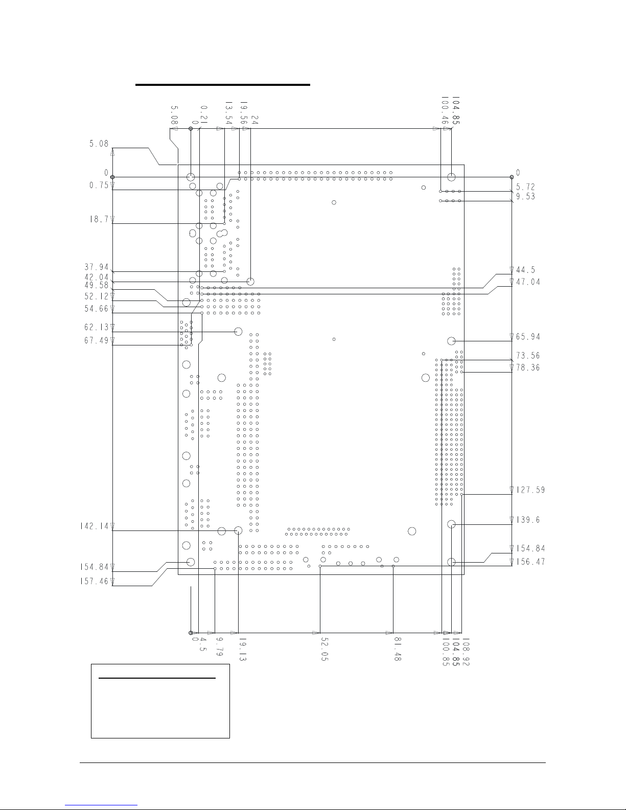
2.7 Mechanical Dimensions
MSEP800 Version V0.3/1.0
Unit: mm (millimeter)
Tolerance: +/- 0.1mm
Date: 24.05.2006
Author: BRR
Page 19
DIGITAL-LOGIC AG MSEP800 Manual V1.0G
19
Page 20
DIGITAL-LOGIC AG MSEP800 Manual V1.0G
20
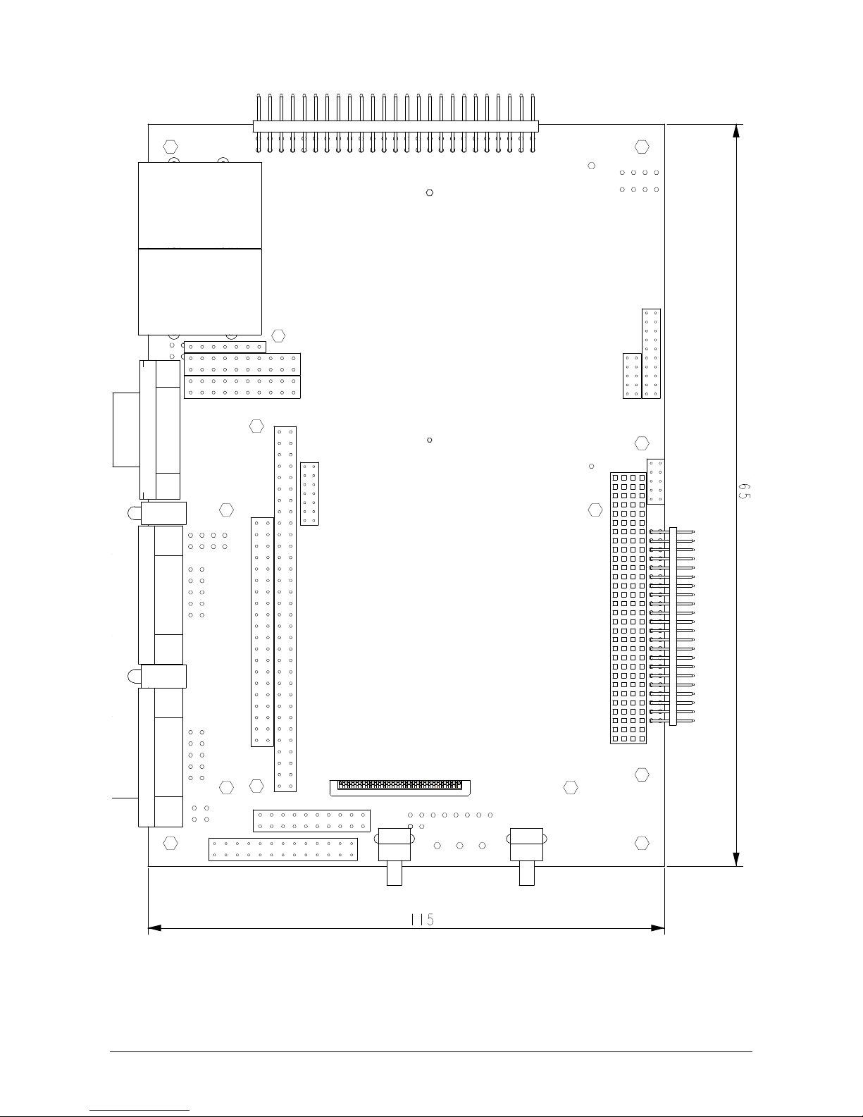
2.7.1 Hole pattern for the MSEP800 board
MSEP800 Version V0.3/1.0
Unit: mm (millimeter)
Tolerance: +/- 0.1mm
Date: 24.05.2006
Author: BRR
Page 21
DIGITAL-LOGIC AG MSEP800 Manual V1.0G
21
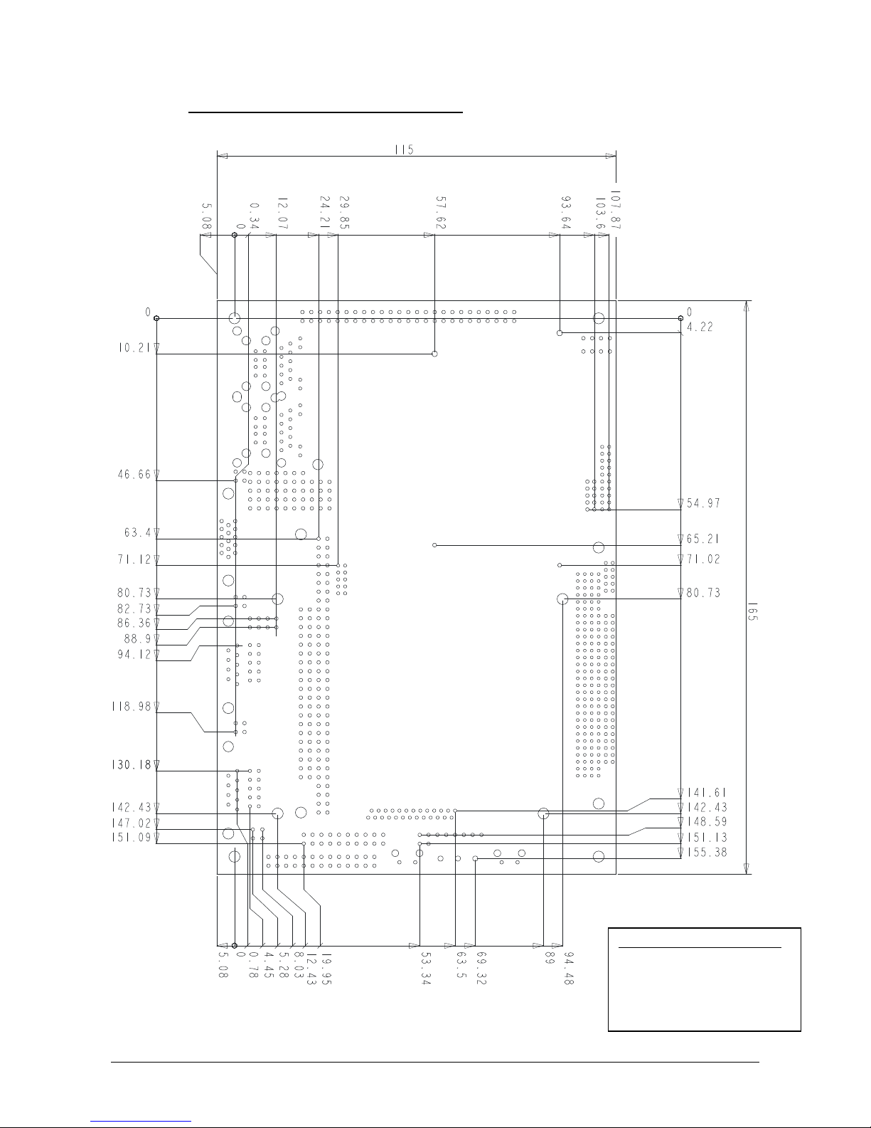
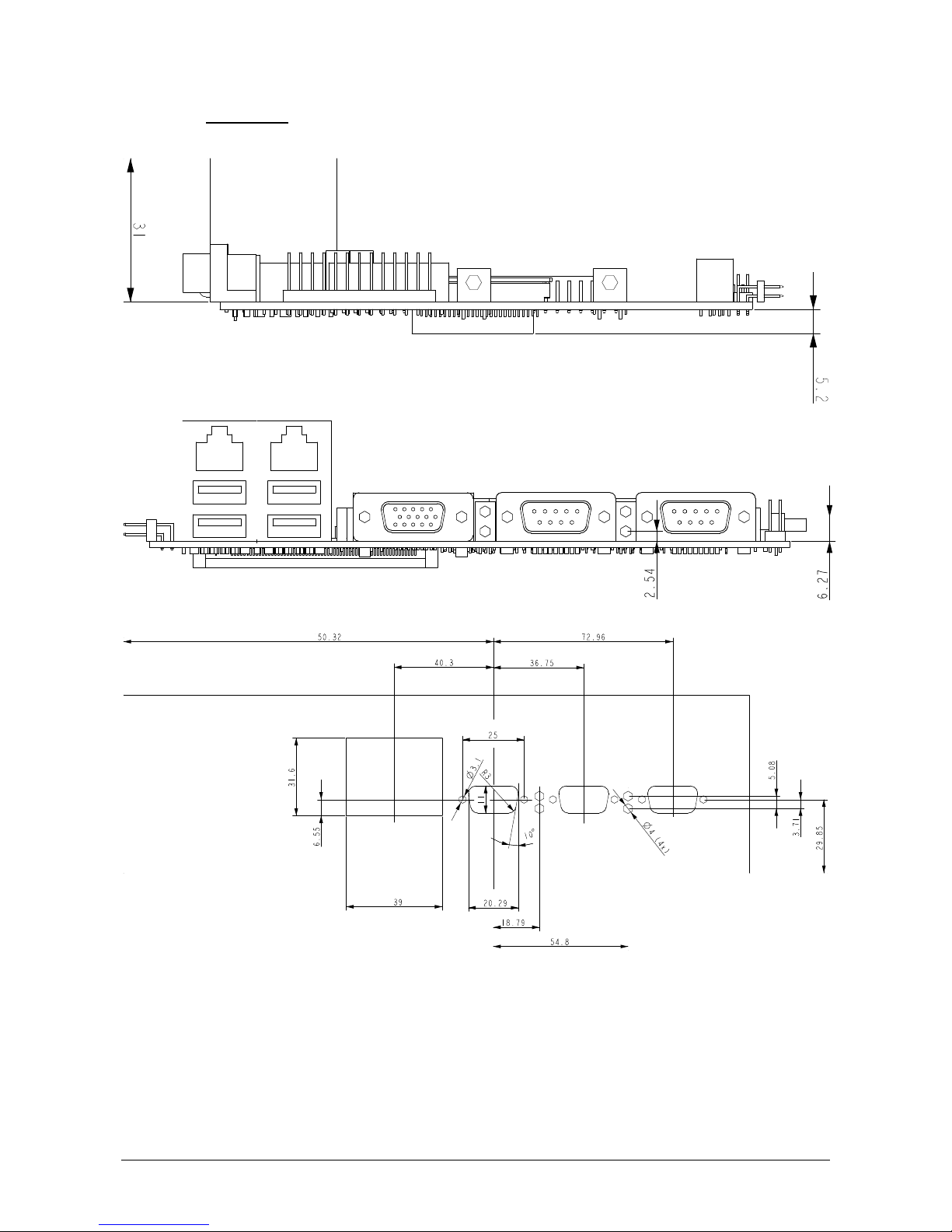
2.7.2 Side View
Page 22
DIGITAL-LOGIC AG MSEP800 Manual V1.0G
22
2.8 MSEP800 Incompatibilities to a standard PC/AT
2.8.1 DVI is not PNP!
If you use the MSEP800 with the MSEP800-M the DVI port is not plug and play.
That means you have to connect the DVI monitor before you turn on the system power.
2.8.2 PC104 BUS / ISA BUS
An onboard LPC to ISA-bridge makes it possible to expand the functionality of the board with
additional PC/104 cards.
Because of the transformation from LPC to ISA it is unfortunately not possible to realize a 16Bit
access. This does not mean that these cards cannot be used, but the 16Bit access is divided into two
accesses. Therefore the access to these cards is a little bit slower.
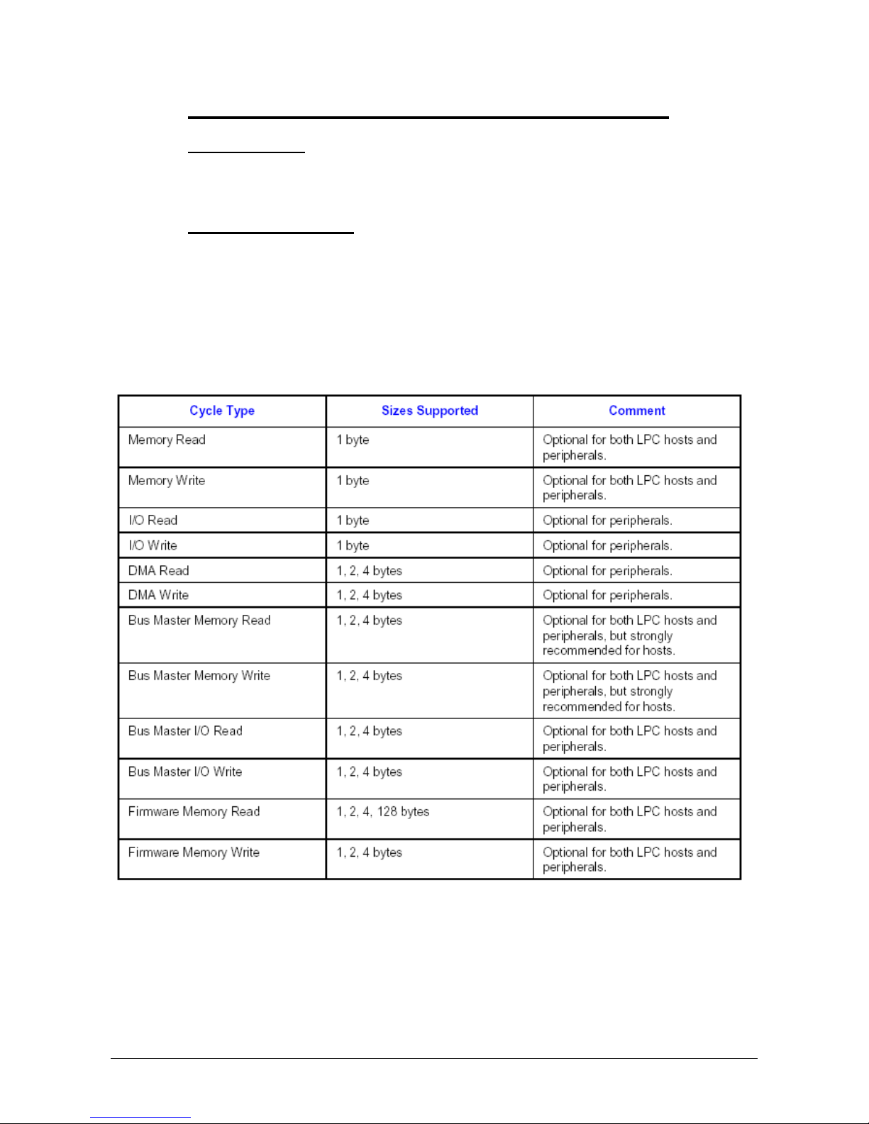
The LPC support the following bus cycles:
That means, all Non-Busmaster I/O and MEM Cycles are only 8Bit wide and never 16Bit wide. 16Bit
datatransfer is available in the BusMaster modus only.
Page 23

DIGITAL-LOGIC AG MSEP800 Manual V1.0G
23
2.8.3 ISA-Incompatibilitiywith ISA-PCCARD-Controller
The experience is, that ATA-Drives controlled in a ISA-PCMCIA Controller are not working.
Solution:
Using a PCCARD-Controller on the PCI-Bus
2.8.4 ISA-Incompatibilitiy with 16Bit I/O Transfer with FPGA-Decoder
The experience is, that 16Bit I/O-transfers decoded with a FPGA are not allways working correct. Each case
must be tested. Specially on odd adresses are problems expected.
Solution:
Using two 8Bit transfer instead one 16Bit transfer. For timecritical transfers is recommended to use the PCIBus.
2.8.5 ISA-Incompatibilitiy with 16Bit Memory Transfer with FPGA-Decoder
The experience is, that 16Bit Memory-transfers decoded with a FPGA are not allways working correct. Each
case must be tested. Specially on odd adresses are problems expected.
Solution:
Using two 8Bit transfer instead one 16Bit transfer. For timecritical transfers is recommended to use the PCIBus.
Page 24

DIGITAL-LOGIC AG MSEP800 Manual V1.0G
24
2.9 MSEP800 Related Application Notes
# Description
80 High frequency Radiation (to meet EN55022)
Application Notes are availble at http://www.digitallogic.com ->support, or on any Application CD from
DIGITAL-LOGIC.
Page 25

DIGITAL-LOGIC AG MSEP800 Manual V1.0G
25
2.10 High Frequency Radiation (to meet EN55022/EN61000)
All peripheral interfaces are filtered to meet the EMI/EMC standards EN55022.
Page 26
DIGITAL-LOGIC AG MSEP800 Manual V1.0G
26
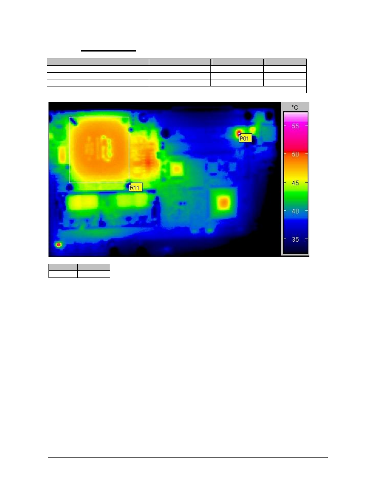
2.11 Thermoscan
Product: Part.Nr. Serial number: Version:
MSEP800
SODIMM DDR 1GB
Software Windows XP SP2 running desktop
t [min] f
CPU
[MHz]
60 500
Page 27
DIGITAL-LOGIC AG MSEP800 Manual V1.0G
27
2.12 RTC Battery-Lifetime
Battery specs:
Lowest temp.
-40°C
Nominal temp.
+20°C
Highest temp.
+85°C
Manufacturer: pba
Type: ER10280
Capacity vers. Temp: 10uA 360mAh 325mAh 220mAh
Voltage vers. Temp. 10uA 3.6V 3.6V Ca. 3.6V
Nominal values: 3.6V / 450mAh @ 0.5mA / -55°C...~+8 5°C
Information taken from the datasheet of ER10280
PRODUCT: Temperatur
°C
Battery voltage V VCC (+12V)
switched ON
µA
VCC (+12V)
switched off
µA
Battery current: +25°C 3.6 0 10
Battery-Lifetime: +25°C >3.5 years >3.5 year
2.12.1 External battery assembling:
If customer wants to connect an external battery (check for the appropriate connector in the chapter
DESCRIPTION OF THE CONNECTORS), then some precautions have to be made:
- The battery is protected from charging. Do not use a charchable battery
The RTC device defines a voltage level of 2.0V...3.6V, so do use an external battery, which will be in this
range (inclusive the diode which is already assembled onboard)
Page 28

DIGITAL-LOGIC AG MSEP800 Manual V1.0G
28
3 BUS SIGNALS
3.1 PC104 Bus
Please note, that the ISA-Bus may have some minor incompatibilities, see chapter 2.10.
AEN, output
Address Enable is used to degate the microprocessor and other devices from the I/O channel to allow DMA
transfers to take place. low = CPU Cycle , high = DMA Cycle
BALE, output
Address Latch Enable is provided by the bus controller and is used on the system board to latch valid addresses and memory decodes from the microprocessor. This signal is used so that devices on the bus can
latch LA17..23. The SA0..19 address lines latched internally according to this signal. BALE is forced high
during DMA cycles.
/DACK[0..3, 5..7], output
DMA Acknowledge 0 to 3 and 5 to 7 are used to acknowledge DMA requests (DRQO through DRQ7). They
are active low. This signal indicates that the DMA operation can begin.
DRQ[0..3, 5..7], input
DMA Requests 0 through 3 and 5 through 7 are asynchronous channel requests used by peripheral devices
and the I/O channel microprocessors to gain DMA service (or control of the system). A request is generated
by bringing a DRQ line to an active level. A DRQ line must be held high until the corresponding DMA Request Acknowledge (DACK/) line goes active. DRQO through DRQ3 will perform 8-Bit DMA transfers; DRQ57 are used for 16 accesses.
/IOCHCK, input
IOCHCK/ provides the system board with parity (error) information about memory or devices on the I/O
channel. low = parity error, high = normal operation
IOCHRDY, input
I/O Channel Ready is pulled low (not ready) by a memory or I/O device to lengthen I/O or memory cycles.
Any slow device using this line should drive it low immediately upon detecting its valid address and a Read
or Write command. Machine cycles are extended by an integral number of one clock cycle (67 nanoseconds). This signal should be held in the range of 125-15600nS. low = wait, high = normal operation
/IOCS16, input
I/O 16 Bit Chip Select signals the system board that the present data transfer is a 16-Bit, 1 wait-state, I/0 cycle. It is derived from an address decode. /IOCS16 is active low and should be driven with an open collector
(300 ohm pull-up) or tri-state driver capable of sinking 20mA. The signal is driven based only on SA15-SAO
(not /IOR or /IOW) when AEN is not asserted. In the 8 Bit I/O transfer, the default transfers a 4 wait-state cycle.
/IOR, input/output
I/O Read instructs an I/O device to drive its data onto the data bus. It may be driven by the system microprocessor or DMA controller, or by a microprocessor or DMA controller resident on the I/O channel. This signal is active low.
/IOW, input/output
I/O Write instructs an I/O device to read the data on the data bus. It may be driven by any microprocessor or
DMA controller in the system. This signal is active low.
Page 29

DIGITAL-LOGIC AG MSEP800 Manual V1.0G
29
IRQ[ 3 - 7, 9 - 12, 14, 15], input
These signals are used to tell the microprocessor that an I/O device needs attention. An interrupt request is
generated when an IRQ line is raised from low to high. The line must be held high until the microprocessor
acknowledges the interrupt request.
/Master, input
This signal is used with a DRQ line to gain control of the system. A processor or DMA controller on the I/0
channel may issue a DRQ to a DMA channel in cascade mode and receive a /DACK.
/MEMCS16, input
MEMCS16 Chip Select signals the system board if the present data transfer is a 1 wait-state, 16-Bit, memory
cycle. It must be derived from the decode of LA17 through LA23. /MEMCS16 should be driven with an open
collector (300 ohm pull-up) or tri-state driver capable of sinking 2OmA.
/MEMR input/output
These signals instruct the memory devices to drive data onto the data bus. /MEMR is active on all memory
read cycles. /MEMR may be driven by any microprocessor or DMA controller in the system. When a microprocessor on the I/0 channel wishes to drive /MEMR, it must have the address lines valid on the bus for one
system clock period before driving /MEMR active. These signals are active low.
/MEMW, input/output
These signals instruct the memory devices to store the data present on the data bus. /MEMW is active in all
memory read cycles. /MEMW may be driven by any microprocessor or DMA controller in the system. When a
microprocessor on the I/O channel wishes to drive /MEMW, it must have the address lines valid on the bus
for one system clock period before driving /MEMW active. Both signals are active low.
OSC, output
Oscillator (OSC) is a high-speed clock with a 70 nanosecond period (14.31818 MHz). This signal is not synchronous with the system clock. It has a 50% duty cycle. OSC starts 100µs after reset is inactive.
RESETDRV, output
Reset Drive is used to reset or initiate system logic at power-up time or during a low line-voltage outage. This
signal is active high. When the signal is active all adapters should turn off or tri-state all drivers connected to
the I/O channel. This signal is driven by the permanent Master.
/REFRESH, input/output
These signals are used to indicate a refresh cycle and can be driven by a microprocessor on the I/0 channel.
These signals are active low.
SAO-SA19, LA17 - LA23 input/output
Address bits 0 through 19 are used to address memory and I/0 devices within the system. These 20 address
lines, allow access of up to 1MBytes of memory. SAO through SA19 are gated on the system bus when
BALE is high and are latched on the falling edge of BALE. LA17 to LA23 are not latched and addresses the
full 16 MBytes range. These signals are generated by the microprocessors or DMA controllers. They may
also be driven by other microprocessor or DMA controllers that reside on the I/0 channel. The SA17-SA23
are always LA17-LA23 address timings for use with the MSCS16 signal. This is advanced AT96 design. The
timing is selectable with jumpers LAxx or SAxx.
/SBHE, input/output
Bus High Enable (system) indicates a transfer of data on the upper byte of the data bus, XD8 through XD15.
Sixteen-Bit devices use /SBHE to condition data-bus buffers tied to XD8 through XD15.
Page 30

DIGITAL-LOGIC AG MSEP800 Manual V1.0G
30
SD[O..15], input/output
These signals provide bus bits 0 through 15 for the microprocessor, memory, and I/0 devices. DO is the
least-significant Bit and D15 is the most significant Bit. All 8-Bit devices on the I/O channel should use DO
through D7 for communications to the microprocessor. The 16-Bit devices will use DO through D15. To support 8-Bit device, the data on D8 through D15 will be gated to DO through D7 during 8-Bit transfers to these
devices; 16-Bit microprocessor transfers to 8-Bit devices will be converted to two 8-Bit transfers.
/SMEMR input/output
These signals instruct the memory devices to drive data onto the data bus for the first MByte. /SMEMR is
active on all memory read cycles. /SMEMR may be driven by any microprocessor or DMA controller in the
system. When a microprocessor on the I/0 channel wishes to drive /SMEMR, it must have the address lines
valid on the bus for one system clock period before driving /SMEMR active. The signal is active low.
/SMEMW, input/output
These signals instruct the memory devices to store the data present on the data bus for the first MByte.
/SMEMW is active in all memory read cycles. /SMEMW may be driven by any microprocessor or DMA controller in the system. When a microprocessor on the I/O channel wishes to drive /SMEMW, it must have the
address lines valid on the bus for one system clock period before driving /SMEMW active. Both signals are
active low.
SYSCLK, output
This is a 8 MHz system clock. It is a synchronous microprocessor cycle clock with a cycle time of 167 nanoseconds. The clock has a 66% duty cycle. This signal should only be used for synchronization.
TC output
Terminal Count provides a pulse when the terminal count for any DMA channel is reached. The TC completes a DMA-Transfer. This signal is expected by the onboard floppy disk controller. Do not use this signal,
because it is internally connected to the floppy controller.
/OWS, input
The Zero Wait State (/OWS) signal tells the microprocessor that it can complete the present bus cycle without inserting any additional wait cycles. In order to run a memory cycle to a 16-Bit device without wait cycles,
/OWS is derived from an address decode gated with a Read or Write command. In order to run a memory
cycle to an 8-Bit device with a minimum of one-wait states, /OWS should be driven active one system clock
after the Read or Write command is active, gated with the address decode for the device. Memory Read and
Write commands to an 8-Bit device are active on the falling edge of the system clock. /OWS is active low
and should be driven with an open collector or tri-state driver capable of sinking 2OmA.
12V +/- 5%
used only for the flatpanel supply.
GROUND = 0V
used for the entire system.
VCC, +5V +/- 0.25V
To supply other PC/104 peripheral cards. Max. current 2Amp.
For further Informations about PC/104 and PC/104plus, please refer to the PC/104 specification
manual which is available on the internet. http://www.digitallogic.com (manuals)
Page 31

DIGITAL-LOGIC AG MSEP800 Manual V1.0G
31
3.2 Addressing PCI Devices :
DEVICE IDSEL PIRQ #REG #GNT Remarks
internal Chipset PCI devices and resources
CPU AD11 A --- ---
CS5536 AD25 A / B / C / D --- ---
external PCI slots
PC/104+ Slot 1 AD26 C / D / A / B 0 0
PC/104+ Slot 2 AD27 D / A / B / C 1 1
PC/104+ Slot 3 AD28 A / B / C / D 2 2
PC/104+ Slot 4 AD29 B / C / D / A 3 3
Separate PCI Controller onboard.
DEVICE IDSEL PIRQ #REQ #GNT Remarks
100Mbit-LAN AD23 B 4 4 Onboard
1Gbit-LAN AD22 A 5 5 Onboard Optional
MiniPCI AD24 C / D 3 3 Onboard Optional
Note:
On board version V2.0 (and newer) only 2 PCI bus master are available (max. 3 PC/104+ cards – 2x
master 1x slave). The reason why ist the change from the LPCtoISA bridge to the PCItoISA bridge.
3.3 Expansion Bus
The bus currents and maxlentgh’s are as follows:
Output Signals: Voltage / Current Max.Length
ISA-BUS * (8Mhz) 5.0V @ 8mA 50cm terminated
PCI-BUS (33MHz) 3.3V 30cm
LPC-Bus 3.3V 2mA 5cm
ATA-HD (33ohm termiantion onboard) 3.3V 20cm
USB 3.3V (Bus) 6meter
* for buslength > 10cm are AC-Bustermination required.
Page 32

DIGITAL-LOGIC AG MSEP800 Manual V1.0G
32
3.3.1 Expansion Bus max. supply currents
The bus different expansions may drive the following supply currents :
At the 5Volt the total max.system current is rated at 6 Amp.
At the 3.3Volt the total max.system current is rated at 6 Amp.
Output Signals: Voltage / Current Max.Current
ISA-BUS (PC/104) 5.0V 2 Amp.
All cards counted together
PCI-BUS (PC/104plus and Risercard) 3.3V 4 Amp.
All cards counted together 5.0V 2 Amp.
USB per connector 5.0V 0.5Amp
All USB together 2 Amp. 1)
Harddisk parallel ATA (PATA) 5.0V 0.6Amp per HD
Total over all harddisk (SATA and PATA) 1.5Amp. max.
1) 2)
Harddisk serial ATA (SATA) 5.0V 0.75Amp. per HD
Total over all harddisk (SATA and PATA 1.5Amp. max
1) 2)
1) The current may be increased, if other peripherals are consuming less (for ex. No PC/104 peripherals are
connected).
2) The Harddisk may be powered externally , if the total 5Volt supply is overloaded.
Page 33

DIGITAL-LOGIC AG MSEP800 Manual V1.0G
33
4 DETAILED SYSTEM DESCRIPTION
This system has a system configuration based on the ISA and PCI architecture. Read carefully all information since this product is a very new computertechnology.
4.1 Power Supply Requirements
This product includes allready a widerange powersupply. So the supply voltage may be in the
range of 8V up to 30V DC.
The recommended supplyinput is 12Volt or 24Volt DC. We recommend to protect the system
with a fuse.
4.1.1 Minimum Power-OFF time:
If the power is switched off, the off period must be minimum 10sec !
All capacitors must be fully discharged befor a new power on is performed.
4.2 Power Requirements
The power is connected through the PC/104 power connector; or the separate power connector on the
board. The supply uses only the +5 Volts and ground connection.
Warning: Make sure that the power plug is wired correctly before supplying power to the
board ! A built-in diode protects the board against reverse polarity.
Testenvironment for powerconsumption measurement:
Peripheries:
Harddisk Hitachi Mod-HTS424020M9AT00 20Gb
Monitor Eizo Flexscan F340i.W
PS/2-KB Logitech Mod-iTouch Keyboard
PS/2-MS Logitech Mod-M-CAA43
Software:
MS-DOS V6.22
WinXP
Current consumption @ 10/19/24Volt supply at –40°C /+25°C/+85°C
Mode Memory
Voltage: -30 °C
+25°C
+85 °C
MSEP800 - 500MHz
[mA]
[mA]
[mA]
Win2000: Desktop
1GB
10V
960
Win2000: Desktop
1GB
19V
520
Win2000: Desktop
1GB
24V
420
Page 34

DIGITAL-LOGIC AG MSEP800 Manual V1.0G
34
4.3 Interface
4.3.1 Keyboard AT Compatible and PS/2 Mouse
ONLY AVAILABLE WITH OPTION 804012
Attention: For the mouse there is a Y-Cable needed !
Pin Signal Pin Signal
Pin 1 = KB_Data Pin 2 = MS_Data
Pin 3 = GND Pin 4 = +5Volt / 100mA
Pin 5 = KB_Clk Pin 6 = MS_Clk
4.3.2 Line Printer Port LPT1
ONLY AVAILABLE WITH OPTION 804012
A standard bi-directional LPT port is integrated into the MICROSPACE PC.
Further information about these signals is available in numerous publications, including the IBM technical
reference manuals for the PC and AT computers and from some other reference documents.
The current is: IOH = 12 mA IOL = 24mA
The SMC 37C672 may be programmed via software commands.
In the NEW BIOS version, this selection may be controled with the BIOS setup screen.
Page 35

DIGITAL-LOGIC AG MSEP800 Manual V1.0G
35
4.3.3 Serial Ports COM1-COM2
The serial channels are fully compatible with 16C550 UARTS. COM1 is the primary serial port, and is supported by the board's ROM-BIOS as the PC-DOS 'COM1' device. The secondary serial port is COM2; it is
supported as the 'COM2' device.
Standard: COM 1/2: SMC 37C672: 2 x 16C550 compatible serial interfaces
Serial Port Connectors COM1, COM2 on 9pin DSUB
DB9 Pin Signal Name Function in/out
1 DCD Data Carrier Detect in
2 RXD Receive Data in
3 TXD Transmit Data out
4 DTR Data TerminalReady out
5 GND Signal Ground
6 DSR Data Set Ready in
7 RTS Request To Send out
8 CTS Clear to Send in
9 RI Ring Indicator
The serial port signals are compatible with the RS232C specifications.
If a second UART is assembled, that means the COM3/4 are available, please refer to chapter 12.2.5
4.3.4 Serial Ports COM3-COM4
ONLY AVAILABLE WITH OPTION 804012
The serial channels are fully compatible with 16C550 UARTS. COM3 is the primary serial port, and is supported by the board's ROM-BIOS as the PC-DOS 'COM3' device. The secondary serial port is COM4; it is
supported as the 'COM4' device.
Standard: COM 3/4: TI 2 x 16C550 compatible serial interfaces
Serial Port Connectors COM1, COM2 on 9pin DSUB
DB9 Pin Signal Name Function in/out
1 DCD Data Carrier Detect in
2 RXD Receive Data in
3 TXD Transmit Data out
4 DTR Data TerminalReady out
5 GND Signal Ground
6 DSR Data Set Ready in
7 RTS Request To Send out
8 CTS Clear to Send in
9 NC
The serial port signals are TTL levels A conveter is needed to provide the Interface standard.
If a second UART is assembled, that means the COM3/4 are available, please refer to chapter 12.2.5
Page 36

DIGITAL-LOGIC AG MSEP800 Manual V1.0G
36
4.3.5 Floppy Disk Interface
The onboard floppy disk controller and ROM-BIOS support one or two floppy disk drives in any of the standard PC-DOS and MS-DOS formats shown in the table .
Supported Floppy Formats
Capacity Drive size Tracks Data rate DOS version
1.2 MB 5-1/4" 80 500 KHz 3.0 - 6.22
720 K 3-1/2" 80 250 KHz 3.2 - 6.22
1.44 M 3-1/2" 80 500 KHz 3.3 - 6.22
Floppy Interface Configuration
The desired configuration of floppy drives (number and type) must be properly initialized in the board's
CMOS - configuration memory. This is generally done by using DEL or F2 at bootup time.
Floppy Interface connector
The table shows the pinout and signal definitions of the board's floppy disk interface connector. It is identical
in pinout to the floppy connector of a standard AT. Note that, as in a standard PC or AT, both floppy drives
are jumpered to the same drive select: as the 'second' drive. The drives are uniquely selected as a result of a
swapping of a group of seven wires (conductors 10-16) that must be in the cable between the two drives.
The seven-wire swap goes between the computer board and drive 'A'; the wires to drive 'B' are unswapped
(or swapped a second time). The 26 pin high density (1mm pitch FCC) connector has only one drive and
motor select. The onboard jumper defines the drive A: or B:. Default is always A:.
Floppy Disk Interface Technology
We only support CMOS drives. That means that the termination resistors are 1 Kohm. 5 1/4“-drives are not
recommended (TTL interface).
The 26 pin Connector: FFC/FPC 0.3mm thick 1.0mm (0.039") pitch (MOLEX 52030 Serie)
Floppy Disk Interface Connector
FD26: Pin Signal Name Function in/out
1 VCC +5 volts
2 IDX Index Pulse in
3 VCC +5 volts
4 DS2 Drive Select 2 out
5 VCC +5 volts
6 DCHG Disk Change in
10 M02 Motor On 2 out
12 DIRC Direction Select out
14 STEP Step out
16 WD Write Data out
17 GND Signal grounds
18 WE Write Enable out
19 GND Signal grounds
20 TRKO Track 0 in
21 GND Signal grounds
22 WP Write Protect in
23 GND Signal grounds
24 RDD Read Data in
25 GND Signal grounds
26 HS Head Select out
4.3.6 Speaker Interface
One of the board's CPU device provides the logic for a PC compatible speaker port. The speaker logic signal
is buffered by a transistor amplifier, and provides approximately 0.1 watt of audio power to an external 8 ohm
speaker. Connect the speaker between VCC and speaker output to have no quiescient current.
Page 37

DIGITAL-LOGIC AG MSEP800 Manual V1.0G
37
4.4 Controllers
4.4.1 Interrupt Controllers
An 8259A compatible interrupt controller, within the chipset, provides seven prioritized interrupt levels. Of
these, several are normally associated with the board's onboard device interfaces and controllers, and several are available on the AT expansion bus.
Interrupt: Sources: Onboard used:
IRQ0 ROM-BIOS clock tick function, from timer 0 Yes
IRQ1 Keyboard controller output buffer full Yes
IRQ2 Used for cascade 2. 8259 Yes
IRQ3 COM2 serial port Yes
IRQ4 COM1 serial port Yes
IRQ5 LPT2 parallel printer (if present) no *
IRQ6 Floppy controller Default = disabled
IRQ7 LPT1 parallel printer Yes
IRQ8 Battery backed clock Yes
IRQ9 Free for user no *
IRQ10 Free for user no *
IRQ11 Free for user no *
IRQ12 PS/2 mouse Yes
IRQ13 Math. coprocessor Yes
IRQ14 IDE Primary channel Yes
IRQ15 IDE Secondary cannel Yes
- * It may depends on the LAN configuration
- ** IRQ 15 = if option CF is not assembled, free for user
4.4.2 Programmable Timer Controller
An 8253 compatible timer/counter device is also included in the board's ASIC device. This device is utilized
in precisely the same manner as in a standard AT implementation. Each channel of the 8253 is driven by a
1.190 MHz clock, derived from a 14.318 MHz oscillator, which can be internally divided in order to provide a
variety of frequencies.
Timer 2 can also be used as a general purpose timer if the speaker function is not required.
Timer Assignment
Timer Function
0 ROM-BIOS clock tick (18.2 Hz)
1 DRAM refresh request timing (15 µs)
2 Speaker tone generation time base
Page 38

DIGITAL-LOGIC AG MSEP800 Manual V1.0G
38
4.4.3 RTC (Real Time Clock)
An AT compatible date/time clock is located within the chipset. The device also contains a CMOS static
RAM, compatible with that in standard ATs. System configuration data is normally stored in the clock chip's
CMOS RAM in a manner consistent with the convention used in other AT compatible computers.
The battery-backed clock can be set by using the DIGITAL-LOGIC AG SETUP at boot-time.
4.4.4 Watchdog
The watchdog timer detects a system crash and performs a hardware reset. After power up, the watchdog is
always disabled as the BIOS does not send strobes to the watchdog. In case that the user wants to take advantage of the watchdog, the application must produce a strobe at least every 800 ms. If no strobe occures
within the 800 ms, the watchdog resets the system.
Please refer to the chapter 12. The watchdog feature is integrated in the INT15 function.
There are also some programming examples available:
Product CD-Rom or customer download area: \tools\SM855\int15dl\…
Page 39

DIGITAL-LOGIC AG MSEP800 Manual V1.0G
39
4.5 BIOS
4.5.1 BIOS History
Version: Date: Status: Modifications:
1.05 03.2006 Final
1.06 05.2006 ISA IRQ reservation
1.07 05.2006 AC97 detection
1.08 05.2006 ISA IRQ table corrected
1.09b 09.2006 USB fix
The bios V1.09b is only for the following board version:
- MSEP800: V0.1, V0.2, V0.3 and V1.0
- MSM800SEV: V1.0, V1.1 and V1.2
1.10b 09.2006 PCI ROUTING TABLE
The bios V1.10b (or newer releases) are only for the following board version:
- MSEP800: V1.1
- MSM800SEV: V2.0 / V2.1
- SM800PCX: V1.0
-
- (or newer board versions)
-
1.12 11.2006 - Video default settings fixed
- RAM memory settings restored
1.13 12.2006 - NumLock
- IRQ15 assignable for ISA
- IRQ6 no more available for PCI
1.14 01.2007 - IT8888 PCI to ISA Bridge
- NumLock Fix
Page 40

DIGITAL-LOGIC AG MSEP800 Manual V1.0G
40
4.5.2 Download CORE-BIOS
Before downloading a BIOS, please check as follows:
- Make a bootable diskette including the following files:
- Flashrom.com
- core BIOS xxxxxxxx.yyy
IMPORTANT:
Do not use boot disks created in a Windows operating system. If you do not have a MSDOS 6.22 disk available, you can download a boot disk from www.bootdisk.com .
NOTE:
- Select the SHADOW option in the BIOS, for a BIOS and VGA (if this option is available).
- Make sure, that the Flashrom.com programm and the BIOS to download are on the
same path and directory!
- Boot the DOS without config.sys & autoexec.bat -> press “F5” while starting DOS boot.
- Is the empty diskspace, where the Fhlashrom.com is located, larger than 64kB (for safe storage)
- Is the floppydisk not write-protected
Start the DOWNLOADING process:
1. Start the system with the bootable diskette. If you do not have a bootable diskette or floppy drive
2. you may can start in DOS mode by pressing the F5 key to disable the autoexec.bat and config.sys.
3. Run Flashrom.com (In some cases you have to ty the following: "FLASHROM /D /sFFFC0000 biosname.xxx")
4. Power off the system
After power on the system, press "F1" to enter the setup, set the default values and “save and leave”
the setup
5. Switch off the system after the download is finished
If the download does not work:
- Check, if no EMM386 is loaded.
- Check, if no peripheral card is in the system, which occupies the same memory range. Disconnect this
card.
If the download is stopped or not completed, make only a warm boot and repeat the steps or download another file. As the video is may shadowed, everything is visible and a cold boot would clear the screen and
nothing would be visible afterwards.
DO NEVER UPDATE A BIOS WITH A USB MEMORY STICK!!
-> THE SYSTEM WILL CRASH DURING THE DOWNLOAD!
PLEASE ONLY USE USB-FLOPPY OR A STANDARD FLOPPY!
Page 41

DIGITAL-LOGIC AG MSEP800 Manual V1.0G
41
4.5.3 ROM-BIOS Sockets
An EPROM socket with 8 Bit wide data access normally contains the board's AT compatible ROM-BIOS. The
socket takes a E82802AC8 EPROM (or equivalent) device. The board's wait-state control logic automatically
inserts four memory wait states in all CPU accesses to this socket. The ROM-BIOS sockets occupies the
memory area from C0000H through FFFFFh; however, the board's ASIC logic reserves the entire area from
C0000h through FFFFFh for onboard devices, so that this area is already usable for ROM-DOS and BIOS
expansion modules. Consult the appropriate address map for the MICROSPACE MSEP800 ROM-BIOS
sockets.
4.5.3.1 Standard BIOS ROM
DEVICE: FWH
MAP: E0000 - FFFFFh Core BIOS 128k
C0000 – C7FFFh VGA BIOS 32k
CC000 - CFFFFh FREE
4.5.4 BIOS CMOS Setup
If wrong setups are memorized in the CMOS-RAM, the default values will be loaded after resetting the
RTC/CMOS-RAM by desoldering the batterie.
If the battery is down, it is always possible to start the system with the default values from the BIOS.
Page 42

DIGITAL-LOGIC AG MSEP800 Manual V1.0G
42
4.6 CMOS RAM Map
Systems based on the industry-standard specification include a battery backed Real Time Clock chip.
This clock contains at least 64 bytes of non-volatile RAM. The system BIOS uses this area to store information including system configuration and initialization parameters, system diagnostics, and the time
and date. This information remains intact even when the system is powered down.
The BIOS supports 128 bytes of CMOS RAM. This information is accessible through I/O ports 70h and
71h. CMOS RAM can be divided into several segments:
Locations 00h - 0Fh contain real time clock (RTC) and status information
Locations 10h - 2Fh contain system configuration data
Locations 30h - 3Fh contain System BIOS-specific configuration data as well as chipset-specific
information
Locations 40h - 7Fh contain chipset-specific information as well as power management configuration
parameters
The following table provides a summary of how these areas may be further divided.
Beginning Ending Checksum Description
00h 0Fh No RTC and Checksum
10h 2Dh Yes System Configuration
2Eh 2Fh No Checksum Value of 10h - 2Dh
30h 33h No Standard CMOS
34h 3Fh No Standard CMOS - SystemSoft Reserved
40h 5Bh Yes Extended CMOS - Chipset Specific
5Ch 5Dh No Checksum Value of 40h - 5Bh
5Eh 6Eh No Extended CMOS - Chipset Specific
6Fh 7Dh Yes Extended CMOS - Power Management
7Eh 7Fh No Checksum Value of 6Fh - 7Dh
Page 43

DIGITAL-LOGIC AG MSEP800 Manual V1.0G
43
Location Description
00h Time of day (seconds) specified in BCD
01h Alarm (seconds) specified in BCD
02h Time of Day (minutes) specified in BCD
03h Alarm (minutes) specified in BCD
04h Time of Day (hours) specified in BCD
05h Alarm (hours) specified in BCD
06h Day of week specified in BCD
07h Day of month specified in BCD
08h Month specified in BCD
09h Year specified in BCD
0Ah Status Register A
Bit 7 = Update in progress
Bits 6-4 = Time based frequency divider
Bits 3-0 = Rate selection bits that define the periodic in-
terrupt rate and output frequency.
0Bh Status Register B
Bit 7 = Run/Halt
0 Run
1 Halt
Bit 6 = Periodic Timer
0 Disable
1 Enable
Bit 5 = Alarm Interrupt
0 Disable
1 Enable
Bit 4 = Update Ended Interrupt
0 Disable
1 Enable
Bit 3 = Square Wave Interrupt
0 Disable
1 Enable
Bit 2 = Calendar Format
0 BCD
1 Binary
Bit 1 = Time Format
0 12-Hour
1 24-Hour
Bit 0 = Daylight Savings Time
0 Disable
1 Enable
0Ch Status Register C
Bit 7 = Interrupt Flag
Bit 6 = Periodic Interrupt Flag
Bit 5 = Alarm Interrupt Flag
Bit 4 = Update Interrupt Flag
Bits 3-0 = Reserved
0Dh Status Register D
Bit 7 = Real Time Clock
0 Lost Power
1 Power
Continued...
Page 44

DIGITAL-LOGIC AG MSEP800 Manual V1.0G
44
CMOS Map Continued...
Location Description
0Eh CMOS Location for Bad CMOS and Checksum Flags
bit 7 = Flag for CMOS Lost Power
0 = Power OK
1 = Lost Power
bit 6 = Flag for CMOS checksum bad
0 = Checksum is valid
1 = Checksum is bad
0Fh Shutdown Code
10h Diskette Drives
bits 7-4 = Diskette Drive A
0000 = Not installed
0001 = Drive A = 360 K
0010 = Drive A = 1.2 MB
0011 = Drive A = 720 K
0100 = Drive A = 1.44 MB
0101 = Drive A = 2.88 MB
bits 3-0 = Diskette Drive B
0000 = Not installed
0001 = Drive B = 360 K
0010 = Drive B = 1.2 MB
0011 = Drive B = 720 K
0100 = Drive B = 1.44 MB
0101 = Drive B = 2.88 MB
11h Reserved
12h Fixed (Hard) Drives
bits 7-4 = Hard Drive 0, AT Type
0000 = Not installed
0001-1110 Types 1 - 14
1111 = Extended drive types
16-44. See location 19h.
bits 3-0 = Hard Drive 1, AT Type
0000 = Not installed
0001-1110 Types 1 - 14
1111 = Extended drive types 16-44.
See
location 2Ah.
See the Fixed Drive Type Parameters Table in Chapter 2 for infor-
mation on drive types 16-44.
13h Reserved
Continued...
Page 45

DIGITAL-LOGIC AG MSEP800 Manual V1.0G
45
CMOS Map Continued...
Location Description
14h Equipment
bits 7-6 = Number of Diskette Drives
00 = One diskette drive
01 = Two diskette drives
10, 11 = Reserved
bits 5-4 = Primary Display Type
00 = Adapter with option ROM
01 = CGA in 40 column mode
10 = CGA in 80 column mode
11 = Monochrome
bits 3-2 = Reserved
bit 1 = Math Coprocessor Presence
0 = Not installed
1 = Installed
bit 0 = Bootable Diskette Drive
0 = Not installed
1 = Installed
15h Base Memory Size (in KB) - Low Byte
16h Base Memory Size (in KB) - High Byte
17h Extended Memory Size in (KB) - Low Byte
18h Extended Memory Size (in KB) - High Byte
19h Extended Drive Type - Hard Drive 0
See the Fixed Drive Type Parameters Table in Chapter 2 for infor-
mation on drive types 16-44.
1Ah Extended Drive Type - Hard Drive 1
See the Fixed Drive Type Parameters Table in Chapter 2 for infor-
mation on drive types 16-44.
1Bh Custom and Fixed (Hard) Drive Flags
bits 7-6 = Reserved
bit 5 = Internal Floppy Diskette Controller
0 = Disabled
1 = Enabled
bit 4 = Internal IDE Controller
0 = Disabled
1 = Enabled
bit 3 = Hard Drive 0 Custom Flag
0 = Disable
1 = Enabled
bit 2 = Hard Drive 0 IDE Flag
0 = Disable
1 = Enabled
bit 1 = Hard Drive 1 Custom Flag
0 = Disable
1 = Enabled
bit 0 = Hard Drive 1 IDE Flag
0 = Disable
1 = Enabled
Continued...
Page 46

DIGITAL-LOGIC AG MSEP800 Manual V1.0G
46
CMOS Map Continued...
Location Description
1Ch Reserved
1Dh EMS Memory Size Low Byte
1Eh EMS Memory Size High Byte
1Fh - 24h Custom Drive Table 0
These 6 bytes (48 bits) contain the following data:
Cylinders
Landing Zone 10 bits
Write Precomp 10 bits
Heads
Sectors/Track 08 bits
1Fh
Byte 0
bits 7-0 = Lower 8 Bits of Cylinders
20h
Byte 1
bits 7-2 = Lower 6 Bits of Landing Zone
bits 1-0 = Upper 2 Bits of Cylinders
21h
Byte 2
bits 7-4 = Lower 4 Bits of Write Precompensation
bits 3-0 = Upper 4 Bits of Landing Zone
22h
Byte 3
bits 7-6 = Reserved
bits 5-0 = Upper 6 Bits of Write Precompensation
23h
Byte 4
bits 7-0 = Number of Heads
24h
Byte 5
bits 7-0 = Sectors Per Track
25h - 2Ah Custom Drive Table 1
These 6 bytes (48 bits) contain the following data:
Cylinders
Landing Zone 10 bits
Write Precomp 10 bits
Heads
Sectors/Track 08 bits
25h
Byte 0
bits 7-0 = Lower 8 Bits of Cylinders
26h
Byte 1
bits 7-2 = Lower 6 Bits of Landing Zone
bits 1-0 = Upper 2 Bits of Cylinders
27h
Byte 2
bits 7-4 = Lower 4 Bits of Write Precompensation
bits 3-0 = Upper 4 Bits of Landing Zone
Continued...
Page 47

DIGITAL-LOGIC AG MSEP800 Manual V1.0G
47
CMOS Map Continued...
Location Description
28h
Byte 3
bits 7-6 = Reserved
bits 5-0 = Upper 6 Bits of Write Precompensation
29h
Byte 4
bits 7-0 = Number of Heads
2Ah
Byte 5
bits 7-0 = Sectors Per Track
2Bh Boot Password
bit 7 = Enable/Disable Password
0 = Disable Password
1 = Enable Password
bits 6-0 = Calculated Password
2Ch SCU Password
bit 7 = Enable/Disable Password
0 = Disable Password
1 = Enable Password
bits 6-0 = Calculated Password
2Dh Reserved
2Eh High Byte of Checksum - Locations 10h to 2Dh
2Fh Low Byte of Checksum - Locations 10h to 2Dh
30h Extended RAM (KB) detected by POST - Low Byte
31h Extended RAM (KB) detected by POST - High Byte
32h BCD Value for Century
33h Base Memory Installed
bit 7 = Flag for Memory Size
0 = 640KB
1 = 512KB
bits 6-0 = Reserved
34h
Minor CPU Revision
Differentiates CPUs within a CPU type (i.e., 486SX vs 486 DX,
vs 486 DX/2). This is crucial for correctly determining CPU
input clock frequency. During a power on reset, Reg DL holds
minor CPU revision.
35h
Major CPU Revision
Differentiates between different CPUs (i.e., 386, 486, Pentium).
This is crucial for correctly determining CPU input clock frequency. During a power on reset, Reg DH holds major CPU
revision.
36h Hotkey Usage
bits 7-6 = Reserved
bit 5 = Semaphore for Completed POST
bit 4 = Semaphore for 0 Volt POST (not currently used)
bit 3 = Semaphore for already in SCU menu
bit 2 = Semaphore for already in PM menu
bit 1 = Semaphore for SCU menu call pending
bit 0 = Semaphore for PM menu call pending
40h-7Fh
Definitions for these locations vary depending on the chipset.
Page 48

DIGITAL-LOGIC AG MSEP800 Manual V1.0G
48
4.7 EEPROM Saved CMOS Setup
The EEPROM has different functions, as listed below:
• Backup of the CMOS-Setup values.
• Storing system informations like: version, production date, customisation of the board, CPU type.
• Storing user/application values.
The EEPROM will be updated automatically after exiting the BIOS setup menu. The system will operate also
without any CMOS battery. While booting up, the CMOS is automatically updated with the EEPROM values.
Press the Esc-key while powering on the system before the video shows the BIOS message and the CMOS
will not be updated.
This would be helpful, if wrong parameters are stored in the EEPROM and the setup of the BIOS does not
start.
If the system hangs or a problem appears, the following steps must be performed:
1. Reset the CMOS-Setup (to reset the Cmos disconnect the battery for at least 10 minutes).
2. Press Esc until the system starts up.
3. Enter the BIOS Setup:
a) load DEFAULT values (F9)
b) enter the settings for the environment
c) exit the setup (F10)
4. Restart the system.
• The user may access the EEPROM through the INT15 special functions. Refer to the chapter SFI func-
tions.
• The system information are read onyl information. To read, use the SFI functions.
Page 49

DIGITAL-LOGIC AG MSEP800 Manual V1.0G
49
4.7.1 EEPROM Memory for Setup
The EEPROM is used for setup and configuration data, stored as an alternative to the CMOS-RTC. Optionally, the EEPROM setup driver may update the CMOS RTC, if the battery is running down and the checksum
error would appear and stop the system. The capacity of the EEPROM is 2 kByte.
Organisation of the 2048Byte EEPROMs:
Address MAP: Function:
0000h CMOS-Setup valid (01=valid)
0001h Reserved
0003h Flag for DLAG-Message (FF=no message)
0010h-007Fh Copy of CMOS-Setup data
0080h-00FFh reserved for AUX-CMOS-Setup
0100h-010Fh Serial-Number
0110h-0113h Production date (year/day/month)
0114h-0117h 1. Service date (year/day/month)
0118h-011Bh 2. Service date (year/day/month)
011Ch-011Fh 3. Service date (year/day/month)
0120h-0122h Booterrors (Autoincremented if any booterror occurs)
0123h-0125h Setup Entries (Autoincremented on every Setup entry)
0126h-0128h Low Battery (Autoincremented everytime the battery is low, EEPROM -> CMOS)
0129h-012Bh Startup (Autoincremented on every poweron start)
0130h Reserved
0131h Reserved
0132h/0133h BIOS Version (V1.4 => [0132h]:= 4, [0133h]:=1)
0134h/0135h BOARD Version (V1.5 => [0124h]:=5, [0125h]:=1)
0136h BOARD TYPE (‘M’=PC/104, ‘E’=Euro, ‘W’=MSWS, ‘S’=Slot, ‘C’=Custom, ‘X’= smart-
Core or smartModule)
0137h CPU TYPE:
(01h=ELAN300/310, 02h=ELAN400, 05h=P5, 08h=P3, 09h=Elan520, 10h=P-M).
0200h-03FFh Reserved
0200h-027Fh Reserved
0400h-07FFh Free for Customer’s use
Page 50

DIGITAL-LOGIC AG MSEP800 Manual V1.0G
50
4.8 Memory & I/O Map
4.8.1 System Memory Map
The X86 CPU used as central processing unit on the MICROSPACE has a memory address space which is
defined by 32 address bits. Therefore, it can address 1 GByte of memory. The memory address MAP is as
follows:
CPU GEODE
Address: Size: Function / Comments:
000000 - 09FFFFh 640 KBytes Onboard DRAM for DOS applications
0A0000 - 0BFFFFh 128 KBytes CGA, EGA, LCD Video RAM 128kB
0C0000 - 0C7FFFh
0C8000 - 0CFFFFh
32 KBytes
32 KBytes
VGA BIOS
Free for user
0D0000 - 0DFFFFh 64 KBytes free for user
0E0000 - 0EBFFFh
0EC000 - 0EFFFFh
32 KBytes
16 KBytes
Bios
BIOS extensions
0F0000 - 0FFFFFh 64 KBytes Core BIOS
100000 - 1FFFFFFh 31 MBytes DRAM for extended onboard memory
4.8.2 System I/O map
The following table details the legacy I/O range for 000h through 4FFh. Each I/O location has a read/write
(R/W) capability.
Note the following abbreviations:
--- Unknown or can not be determined.
Yes Read and write the register at the indicated
location. No shadow required.
WO Write only. Value written can not be read back.
Reads do not contain any useful information.
RO Read only. Writes have no effect.
Shw The value written to the register can not be read back via the same I/O location. Read back is
accomplished via a “Shadow” register located in MSR space.
Shw@ Reads of the location return a constant or meaningless value.
Shw$ Reads of the location return a status or some other meaningful information.
Rec Writes to the location are “recorded” and written
to the LPC. Reads to the location return the
recorded value. The LPC is not read.
Page 51

DIGITAL-LOGIC AG MSEP800 Manual V1.0G
51
I/O Addr. Function Size R/W Comment
000h Slave DMA Address - Channel 0 8-bit Yes 16-bit values in two transfers.
001h Slave DMA Counter - Channel 0 8-bit Yes 16-bit values in two transfers.
002h
Slave DMA Address - Channel 1 8-bit Yes 16-bit values in two transfers.
003h
Slave DMA Counter - Channel 1 8-bit Yes 16-bit values in two transfers.
004h
Slave DMA Address - Channel 2 8-bit Yes 16-bit values in two transfers.
005h
Slave DMA Counter - Channel 2 8-bit Yes 16-bit values in two transfers.
006h
Slave DMA Address - Channel 3 8-bit Yes 16-bit values in two transfers.
007h
Slave DMA Counter - Channel 3 8-bit Yes 16-bit values in two transfers.
008h
Slave DMA Command/Status - Channels
[3:0]
8-bit Shw$
009h
Slave DMA Request - Channels [3:0] 8-bit WO Reads return value B2h.
00Ah
Slave DMA Mask - Channels [3:0] 8-bit Shw@ Reads return value B2h.
00Bh
Slave DMA Mode - Channels [3:0] 8-bit Shw@ Reads return value B2h.
00Ch
Slave DMA Clear Pointer - Channels [3:0] 8-bit WO Reads return value B2h.
00Dh
Slave DMA Reset - Channels [3:0] 8-bit WO Reads return value B2h.
00Eh
Slave DMA Reset Mask - Channels [3:0] 8-bit Shw@ Reads return value B2h.
00Fh Slave DMA General Mask - Channels [3:0] 8-bit Shw@ Reads return value B2h.
010h-
01Fh
No Specific Usage --- --020h
PIC Master - Command/Status 8-bit Shw$
021h
PIC Master - Command/Status 8-bit Shw$
022h-
03Fh
No Specific Usage --- --040h
PIT – System Timer 8-bit Shw$
041h
PIT – Refresh Timer 8-bit Shw$
042h
PIT – Speaker Timer 8-bit Shw$
043h
PIT – Control 8-bit Shw$
044h-
05Fh
No Specific Usage --- ---
If KEL Memory Offset 100h[0] =
1(EmulationEnable bit).
060h
Keyboard/Mouse - Data Port 8-bit Yes
If MSR 5140001Fh[0] = 1 (SNOOP bit) and
KEL Memory Offset 100h[0] = 0 (EmulationEnable bit).
061h
Port B Control 8-bit Yes
062h-
063h
No Specific Usage --- ---
If KEL Memory Offset 100h[0] = 1
(EmulationEnable bit).
.
064h Keyboard/Mouse - Command/ Status 8-bit Yes
If MSR 5140001Fh[0] = 1 (SNOOP
bit) and KEL Memory Offset 100h[0]
= 0 (EmulationEnable bit)
065h-
06Fh
No Specific Usage --- --070h-
071h
RTC RAM Address/Data Port 8-bit Yes Options per MSR 51400014h[0]. (Note 1)
072h-
073h
High RTC RAM Address/Data Port 8-bit Yes Options per MSR 51400014h[1].
074h-
077h
No Specific Usage --- --078h-
07Fh
No Specific Usage --- --080h
Post Code Display 8-bit Rec Write LPC and DMA. Read only DMA.
081h
DMA Channel 2 Low Page
082h
DMA Channel 3 Low Page
083h
DMA Channel 1 Low Page
8-bit Rec
Upper addr bits [23:16]. Write LPC and
DMA. Read only DMA.
084h-
086h
No Specific Usage 8-bit Rec Write LPC and DMA. Read only DMA.
Page 52

DIGITAL-LOGIC AG MSEP800 Manual V1.0G
52
I/O Addr. Function Size R/W Comment
087h
DMA Channel 0 Low Page 8-bit Rec
Upper addr bits [23:16]. Write LPC and DMA.
Read only DMA.
088h No Specific Usage 8-bit Rec Write LPC and DMA. Read only DMA.
089h DMA Channel 6 Low Page
08Ah
DMA Channel 7 Low Page
08B
DMA Channel 5 Low Page
8-bit Rec
Upper addr bits [23:16]. Write LPC and DMA.
Read only DMA.
08Ch-
No Specific Usage 8-bit Rec Write LPC and DMA. Read only
08Eh DMA.
08Fh
DMA C4 Low Page 8-bit Rec
Upper addr bits [23:16]. See comment at
080h.
090h-
091h
No Specific Usage --- --092h
Port A 8-bit Yes
If kel_porta_en is enabled, then access Port
A; else access LPC.
093h-
09Fh
No Specific Usage --- --0A0h
PIC Slave - Command/Status 8-bit Shw$
0A1h
PIC Slave - Command/Status 8-bit Shw$
0A2h-
0BFh
No Specific Usage 8-bit --0C0h
Master DMA Address - Channel 4 8-bit Yes 16-bit values in two transfers.
0C1h
No Specific Usage 8-bit --0C2h
Master DMA Counter - Channel 4 8-bit Yes 16-bit values in two transfers.
0C3h
No Specific Usage 8-bit --0C4h
Master DMA Address - Channel 5 8-bit Yes 16-bit values in two transfers.
0C6h
Master DMA Counter - Channel 5 8-bit Yes 16-bit values in two transfers.
0C7h
No Specific Usage 8-bit --0C8h
Master DMA Address - Channel 6 8-bit Yes 16-bit values in two transfers.
0CAh
Master DMA Counter - Channel 6 8-bit Yes 16-bit values in two transfers.
0CBh
No Specific Usage 8-bit --0CCh
Master DMA Address - Channel 7 8-bit Yes 16-bit values in two transfers.
0CDh
No Specific Usage 8-bit --0CEh
Master DMA Counter - Channel 7 8-bit Yes 16-bit values in two transfers.
0CFh
No Specific Usage 8-bit --0D0h
Master DMA Command/Status – Channels
[7:4]
8-bit Shw$
0D1h
No Specific Usage 8-bit --0D2h
Master DMA Request - Channels [7:4] 8-bit WO
0D3h
No Specific Usage 8-bit --0D4h
Master DMA Mask - Channels [7:4] 8-bit Yes
0D5h
No Specific Usage 8-bit --0D6h
Master DMA Mode - Channels [7:4] 8-bit Shw@
0D7h
No Specific Usage 8-bit --0D8h Master DMA Clear Pointer - Channels [7:4] 8-bit WO
0D9h
No Specific Usage 8-bit --0DAh
Master DMA Reset - Channels [7:4] 8-bit WO
0DBh
No Specific Usage 8-bit --0DCh
Master DMA Reset Mask - Channels [7:4] 8-bit WO
0DDh
No Specific Usage 8-bit --0DEh
Master DMA General Mask - Channels [7:4] 8-bit Shw@
0DFh
No Specific Usage 8-bit --0E0h-2E7h No Specific Usage --- ---
Page 53

DIGITAL-LOGIC AG MSEP800 Manual V1.0G
53
I/O Addr. Function Size R/W Comment
2E8h-2EFh UART/IR - COM4 8-bit ---
MSR bit enables/disables into I/O
2EFh space.(UART1 MSR
51400014h[18:16], UART2 MSR
51400014h[22:20]). Defaults to
LPC.
2F0h-2F7h No Specific Usage --- ---
2F8h-2FFh UART/IR - COM2 8-bit ---
MSR bit enables/disables into I/O
2FFh space.(UART1 MSR
51400014h[18:16], UART2 MSR
51400014h[22:20]). Defaults to
LPC.
300h- 36Fh No Specific Usage --- --370h
Floppy Status R A 8-bit RO Second Floppy.
371h
Floppy Status R B 8-bit RO Second Floppy.
372h
Floppy Digital Out 8-bit Shw@ Second Floppy.
373h
No Specific Usage 8-bit --374h
Floppy Cntrl Status 8-bit RO Second Floppy.
375h
Floppy Data 8-bit Yes Second Floppy.
376h
No Specific Usage 8-bit --377h
Floppy Conf Reg 8-bit Shw$ Second Floppy.
378h-3E7h No Specific Usage --- ---
3E8h-3EFh UART/IR - COM3 8-bit ---
MSR bit enables/disables into I/O
3EFh space.(UART1 MSR
51400014h[18:16], UART2 MSR
51400014h[22:20]). Defaults to
LPC.
3F0h
Floppy Status R A 8-bit RO First Floppy.
3F1h
Floppy Status R B 8-bit RO First Floppy.
3F2h
Floppy Digital Out 8-bit Shw@ First Floppy.
3F3h
No Specific Usage 8-bit --3F4h
Floppy Cntrl Status 8-bit RO First Floppy.
3F5h Floppy Data 8-bit Yes First Floppy.
3F6h
No Specific Usage 8-bit --3F7h
Floppy Conf Reg 8-bit Shw$ First Floppy.
3F8h-3FFh UART/IR - COM1 8-bit ---
MSR bit enables/disables into I/O
3FFh space.(UART1 MSR
51400014h[18:16], UART2 MSR
51400014h[22:20]). Defaults to
LPC.
480h
No Specific Usage 8-bit WO Write LPC and DMA. Read only DMA.
481h
DMA Channel 2 High Page 8-bit Rec
Upper addr bits [31:24]. Write LPC and DMA.
Read only DMA.
482h DMA Channel 3 High Page
483h DMA Channel 1 High Page
484h-486h No Specific Usage 8-bit WO Write LPC and DMA. Read only DMA.
487h
DMA Channel 0 High Page 8-bit Rec
Upper addr bits [31:24]. Write LPC and DMA.
Read only DMA.
489h
DMA Channel 6 High Page 8-bit Rec
Upper addr bits [31:24]. Write LPC and DMA.
Read only DMA.
48Ah DMA Channel 7 High Page
48Bh DMA Channel 5 High Page
48Ch-48Eh No Specific Usage 8-bit WO Write LPC and DMA. Read only DMA.
Page 54

DIGITAL-LOGIC AG MSEP800 Manual V1.0G
54
I/O Addr. Function Size R/W Comment
48Fh
DMA Channel 4 High Page 8-bit Rec
Upper addr bits [31:24]. Write LPC and DMA.
Read only DMA.
490h-4CFh No Specific Usage --- --4D0h
PIC Level/Edge 8-bit Yes IRQ0-IRQ 7.
4D1h
PIC Level/Edge 8-bit Yes IRQ8-IRQ15.
4D2h-4FFh No Specific Usage --- ---
Note 1. The Diverse Device snoops writes to this port and maintains the MSB as NMI enable. When low, NMI is enabled.
When high, NMI is disabled. This bit defaults high. Reads of this port return bits [6:0] from the on-chip or off-chip
target, while bit 7 is returned from the “maintained” value.
Page 55

DIGITAL-LOGIC AG MSEP800 Manual V1.0G
55
4.9 VGA, LCD
4.9.1 VGA / LCD Controller of the GEODE LX800
• Highly integrated Flat Panel and CRT GUI Accelerator & Multimedia Engine, Palette/DAC, Clock Synthe-
sizer, and integrated frame buffer
• HiQColorTM Technology implemented with TMED (Temporal Modulated Energy Distribution)
• Hardware Windows Acceleration
• Integrated composite NTSC / PAL Support
• Hardware Multimedia Support
• High-Performance Flat Panel Display resolution and color depth at 3.3V
• 24-bit direct interface to color TFT panels
• Advanced Power Management features minimize power usage in:
- Normal operation
– Standby (Sleep) modes
– Panel-Off Power-Saving Mode
• VESA Standards supported
• Fully Compatible with IBM® VGA
• Driver Support for Windows XP, Windows 2000, Windows 98, Windows NT4.0
4.9.2 Graphic modes
Bios settings: 254Mb Video Memory (shared)
Resolution: Col. Dept.: Frequency:
800x600 16Bit / 32Bit 60Hz – 1000Hz
1024x768 16Bit / 32Bit 60Hz – 1000Hz
1152x864 16Bit / 32Bit 60Hz – 1000Hz
1280x1024 16Bit / 32Bit 60Hz – 1000Hz
1600x1200 16Bit / 32Bit 60Hz – 1000Hz
1920x1440 16Bit / 32Bit 60Hz – 85Hz
-> TFT 1600x1200, 60Hz, 32Bit
Page 56

DIGITAL-LOGIC AG MSEP800 Manual V1.0G
56
4.10 LVDS-Display
There a different LCD-Panels available with 6bit-LVDS interface, they can adapted directly to the LVDSInterface of the GEODE videocontroller.
The LVDS interface is composed with:
6 Bit LVDS Datalines
2 Bit LVDS Clocklines
Backligthenable (5V or DC Mainl)
LCD-Supply (VDD) 5V or 3.3V Supply (Enable (3.3V digital))
There is a list of LVDS-Panels:
Display Part.No. Size: Resolution: Colors: Luminance: Power: Remarks:
with 3x6Bit
LVDS or 18Bit
LVDS
Thoshiba:
LTM06C310 6.3” 1024x768 262k 150 cd/m3 3W Tested, limited available
LTM10C306L 10.4” 1024x768 262k 200cd/m3 3W Tested
SIEMENS I-SFT
G23916-B65-H068 10.4” 1024x768 262k 1000cd/m3 20W
NEC 1)
NL10276BC24-13 12.1” 1024x768 262k/16M 400cd/m3 8/6Bit LCD 1)
NL8060BC31-28D 12.1” 800x600 262k 350cd/m3 1)
NL10276BC26-17 10.4” 1024x768 262k 1)
NL10276BC16-01 8.4” 1024x768 262k/16M 8/6Bit LCD 1)
NL10276BC12-02 6.3” 1024x768 262k/16M 8/6Bit LCD 1)
SANYO-TORISAN
TM121XG-02L01 12.1” 1024x768 262k 150cd/m3
TM100SV-02L02 10” 800x600 262k 170cd/m3
LG-Philips LCD
LP104S5 10,4” 800x600 262k 170cd/m3 -T with 300cd/m3
LB150X06 15.0” 1024x768 262k 250cd/m3
For using NEC Panels, please ask the factors for the application-note.
Page 57

DIGITAL-LOGIC AG MSEP800 Manual V1.0G
57
4.11 Boot Time
System Boot-Times
Definitionen/Boot-Medium
Quick
Boot*
Normal
Boot
MSEP005MHz with RTC-Backup battery
Memory 1024MB shared 24MB for Video
Measured device set first in the boot order configuration
time [s]
Boot from Floppy Drive (MS-DOS startup disk) 38
Boot from USB-Floppy Drive (MS-DOS startup disk) 28
Boot from Harddisk to Windows XP Desktop (only Windows installed) 50
Boot from USB Flash Drive (SanDisk Cruzer Micro 1GB) 19
Page 58

DIGITAL-LOGIC AG MSEP800 Manual V1.0G
58
4.12 Mini PCI socket
4.12.1 Type IIIA Form Factor
The Type IIIA form factor supports a card that is not placed at the outer edge of the host
system. The form factor for Type IIIA differs from that of Type IIIB in that Type IIIA
has a larger Y dimension. The form factor for Type IIIA is further characterized by the
following guidelines:
· All dimensions are in millimeters, unless otherwise specified.
· All dimension tolerances are ±.15 mm, unless otherwise specified.
· Dimensions marked with an asterisk (*) are overall envelope dimensions and include
space allowances for insulation to comply with regulatory and safety requirements.
· Insulating material shall not interfere with or obstruct mounting holes or grounding
pads.
· Although illustrates a Type IIIA configuration with both a modem and a
LAN connector, acceptable configurations are for modem only, LAN only, and LAN
and modem combinations (as shown). The location of each connector remains the
same for each configuration.
Page 59

DIGITAL-LOGIC AG MSEP800 Manual V1.0G
59
4.12.2 Type IIIB Form Factor
The Type IIIB form factor supports a card that is not placed at the outer edge of the host
system. The form factor for Type IIIB differs from that of Type IIIA in that Type IIIB
has a smaller Y dimension. The form factor for Type IIIB is further characterized by the
following guidelines:
· All dimensions are in millimeters, unless otherwise specified.
· All dimension tolerances are ±.15 mm, unless otherwise specified.
· Dimensions marked with an asterisk (*) are overall envelope dimensions and include
space allowances for insulation to comply with regulatory and safety requirements.
· Insulating material shall not interfere with or obstruct mounting holes or grounding
pads.
· Although illustrates a Type IIIB configuration with both a modem and a
LAN connector, acceptable configurations are for modem only, LAN only, and LAN
and modem combinations (as shown). The location of each connector remains the
same for each configuration.
Page 60

DIGITAL-LOGIC AG MSEP800 Manual V1.0G
60
5 DESCRIPTION AND LOCATION OF THE CONNECTORS
5.1 Description of the connectors
5.1.1 MSEP800 V1.0
Connector Texture Pin Remarks
X8 DC-Main 3
X2 LVDS / Digital I/O 2x25 RM2.54mm
J32 LAN B 1Gb / USB 3 / 4
J31 LAN A 100Mb USB 1 / 2
X1 VGA 15 HDsub 15
J17 COM2 (RS232) 9 DB9M
J12 COM1 (RS232) 9 DB9M
J21 Printer (LPT) 26 RM2.54mm
J25 COM 3 (TTL)/ COM 4 (TTL) / AC97 2x10 RM2.54mm
J22 Floppy
J8 IDE 2x22 RM2mm
J19 Video IN 4 RM2.54mm
X9* Video Data IN 2x13 RM2mm
J33 PC104+ 4x30
J24 PC104 2x20/2x32
J10 POD Port 2x7 RM2mm
J47 A/D Converter 2x5 RM2.54mm
J30 JTAG 2x5 RM2mm
J38 PIC 2x5 RM2mm
J16 COM 4 (RS232) 2x5 RM2.54mm
J11 COM 3 (RS232) 2x5 RM2.54mm
X5 KB/MS – PS/2 7 RM2.54mm
J5 LCD 10 RM2.54mm
J7 LCD 10 RM2.54mm
J6 LCD 10 RM2.54mm
J4 LCD 10 RM2.54mm
X6 MINI PCI
X7 Power output connector 4 Molex
J20 IrDa 4 RM2.54mm
X3 FAN 1 3 RM2.54mm
X4 External Reset 2 RM2.54mm
X10 Compact Flash socket
J14 10k-Temperatursensor Input 1 (Case) 2 RM2.54mm
J15 10k-Temperatursensor Input 2 (Supply) 2 RM2.54mm
J1 SODIMM RAM socket
Remarks:
Page 61

DIGITAL-LOGIC AG MSEP800 Manual V1.0G
61
5.1.2 MSEPxxxCON-I
Connector Texture Pin Remarks
J4 COM 3 piggy connector 20 RM2.54
J5 COM 4 piggy connector 20 RM2.54
X2 COM 3 DSUB9
X3 LPT DSUB25
X4 COM 4 10 RM2.54
X5 PS/2 connector 10 PS/2
J1 DVO Interface to base board 10 RM2.54
J2 Sound / COM3/4 signals to base board 20 RM2.54
J3 LPT signals to base board 26 RM2.54
X1 Utility connector (KB / MS / Reset…) to base board 8 RM2.54
5.1.3 MSEP800CON-M
Connector Texture Pin Remarks
P1 DVI DVI
X5 MIC IN 3 3.5mm Jack
X8 Line IN 3 3.5mm Jack
X9 Line OUT 3 3.5mm Jack
X4 SPDIF Optical
X6 Utility connector (KB / MS / Reset…) to base board 8 RM2.54
X1 DVO Interface to base board 10 RM2.54
X2 DVO Interface to base board 10 RM2.54
X6 DVO Interface to base board 10 RM2.54
X7 DVO Interface to base board 10 RM2.54
X3 Sound signals to base board 20 RM2.54
Page 62

DIGITAL-LOGIC AG MSEP800 Manual V1.0G
62
5.2 Connector Plan
5.2.1 MSEP800 V1.0
Page 63

DIGITAL-LOGIC AG MSEP800 Manual V1.0G
63
Page 64

DIGITAL-LOGIC AG MSEP800 Manual V1.0G
64
5.2.2 MSEPCON-I
The MSEPCON-I can be use on the MSEP800 V0.3 and V1.0
5.2.3 MSEPCON-M
MSEPCON-M for V0.3 and V1.0
Page 65

DIGITAL-LOGIC AG MSEP800 Manual V1.0G
65
5.3 Power Supply Connectors
X8 Power Input Channel (EMI filtered)
Pin Signal Pin Signal
Pin 1 = 8V – 30V DC-Input Power Input
Pin 2 = earth, masse Systemearth
Pin 3 = 0V DC-Input Ground
X4 = SL-SMT 5.08/90F (Part number: 1837640000) www.weidmueller.com
The counterpart of the X8 is a:
BLZ 5.08/3F SN SW (Part number: 1803050000) available from www.weidmueller.com
5.3.1 Important: Protecting the power supply with fuses!
Protect the system from overcurrent with a fuse in the DC-Supply ! Use
the optional MSEPPWR-Board with EMI filter , overcurrent protection ,
wrong polarity protection and overvoltageprotection.
Without using a fuse, the system will be destroyed in the case of a
overcurrent. Specially in battery supplied applications, like car’s, ther
may be a serious danger because the very high short circuit current.
The system may become very hot or even began to fire, if no fuses are
limiting the max. current. It is recommended to limit the current on a
double normal value.
DC-Input at 12V use a 10 Amp. Fuse.
DC-Input at 24V use a 5 Amp. Fuse.
For the +/-12V use a 1Amp. Fuse.
Page 66

DIGITAL-LOGIC AG MSEP800 Manual V1.0G
66
5.4 Other Connectors on board
J21 Header 0.1” Printerport (EMI-Filtered)
The printer connector provides an interface for 8 Bit centronics printers.
Header onboard: D-SUB connector: Signal
Pin 1 Pin 1 = Strobe
Pin 3 Pin 2 = Data 0
Pin 5 Pin 3 = Data 1
Pin 7 Pin 4 = Data 2
Pin 9 Pin 5 = Data 3
Pin 11 Pin 6 = Data 4
Pin 13 Pin 7 = Data 5
Pin 15 Pin 8 = Data 6
Pin 17 Pin 9 = Data 7
Pin 19 Pin 10 = Acknowledge
Pin 21 Pin 11 = Busy
Pin 23 Pin 12 = paper end
Pin 25 Pin 13 = select
Pin 2 Pin 14 = autofeed
Pin 4 Pin 15 = error
Pin 6 Pin 16 = init printer
Pin 8 Pin 17 = shift in (SI)
Pin 10,12,14,16,18 Pin 18 - 22 = left open
Pin 20,22,24 Pin 23 - 25 = GND
Pin 26 - = VCC 5
J31 USB1 / USB2 and 100M-LAN (EMI-Filtered)
This is a combined connector integrating 2x USB and 1x RJ45 plus the LAN-Magnetics/LED’s
Pin Signal Pin Signal
Pin 1 = VCC5 / 0.5A Pin 5 = VCC5 / 0.5A
Pin 2 = USB-Px- Pin 6 = USB-PxPin 3 = USB-Px+ Pin 7 = USB-Px+
Pin 4 = GND Pin 8 = GND
Pin 1 = TXD0+ Pin 2 = TXD0Pin 3 = TXD1+ Pin 4 = n.c.
Pin 5 = n.c. Pin 6 = TXD1Pin 7 = n.c. Pin 8 = n.c.
J32 USB3 / USB4 and 1G-LAN (EMI-Filtered)
This is a combined connector integrating 2x USB and 1x RJ45 plus the LAN-Magnetics/LED’s
Pin Signal Pin Signal
Pin 1 = VCC5 / 0.5A Pin 5 = VCC5 / 0.5A
Pin 2 = USB-Px- Pin 6 = USB-PxPin 3 = USB-Px+ Pin 7 = USB-Px+
Pin 4 = GND Pin 8 = GND
Pin 1 = TXD0+ Pin 2 = TXD0Pin 3 = TXD1+ Pin 4 = TXD2+
Pin 5 = TXD2- Pin 6 = TXD1Pin 7 = TXD3+ Pin 8 = TXD3-
Page 67

DIGITAL-LOGIC AG MSEP800 Manual V1.0G
67
J12 DSUB9 Serial Port COM1 RS232 (EMI-Filtered)
Header onboard: D-SUB connector:: Signal
Pin 1 = DCD
Pin 6 = DSR
Pin 2 = RxD
Pin 7 = RTS
Pin 3 = TxD
Pin 8 = CTS
Pin 4 = DTR
Pin 9 = RI
Pin 5 = GND
= open
J17 DSUB9 Serial Port COM2 RS232 (EMI-Filtered)
Header onboard: D-SUB connector:: Signal
Pin 1 = DCD
Pin 6 = DSR
Pin 2 = RxD
Pin 7 = RTS
Pin 3 = TxD
Pin 8 = CTS
Pin 4 = DTR
Pin 9 = RI
Pin 5 = GND
= open
J11 Header 0.1” Serial Port COM 3 RS232(EMI-Filtered)
Header onboard: D-SUB connector:: Signal
Pin 1 Pin 1 = DCD
Pin 2 Pin 6 = DSR
Pin 3 Pin 2 = RxD
Pin 4 Pin 7 = RTS
Pin 5 Pin 3 = TxD
Pin 6 Pin 8 = CTS
Pin 7 Pin 4 = DTR
Pin 8 Pin 9 = RI
Pin 9 Pin 5 = GND
Pin10 = open
Attention! On V0.3 the signals of J11 are the same as on J12 (both COM1)
J16 Header 0.1” Serial Port COM4 RS232 (EMI-Filtered)
Header onboard: D-SUB connector:: Signal
Pin 1 Pin 1 = DCD
Pin 2 Pin 6 = DSR
Pin 3 Pin 2 = RxD
Pin 4 Pin 7 = RTS
Pin 5 Pin 3 = TxD
Pin 6 Pin 8 = CTS
Pin 7 Pin 4 = DTR
Pin 8 Pin 9 = RI
Pin 9 Pin 5 = GND
Pin10 = open
Attention! On V0.3 the signals of J16 are the same as on J17 (both COM2)
Page 68

DIGITAL-LOGIC AG MSEP800 Manual V1.0G
68
X1 VGA Monitor (EMI filtered)
X1 Connector 15 pins HiDensity DSUB
Signal Pin Signal
VGA red Pin 1 Red
VGA green Pin 2 Green
VGA blue Pin 3 Blue
Horizontal Synch Pin 13 H-Synch
Vertical Synch Pin 14 V-Synch
Pin 5 + 11 Bridged
Ground Pin 5, 6, 7, 8 Ground
n.c.
n.c.
DDC-Data Pin 12 DDC- Data
DDC-Clock Pin 15 DDC- Clock
J4 /J5 / J6 / J7 DVO Interface
Pin Signal Name Pin Signal Name
J4 J5
1 LCD - DE 1 LCD – FP1
2 LCD - HSYNC 2 LCD – FP2
3 LCD - VSYNC 3 LCD – FP3
4 LCD - SHFCLK 4 LCD – CRT_SCL
5 GND 5 LCD – CRT_SDA
6 LCD - P24V1 6 GND
7 LCD - P24V1 7 VCC3
8 GND 8 VCC3
9 LCD - ENABKL 9 LCD – FP4
10 LCD - FP0 10 LCD – FP5
J6 J7
1 LCD – FP6 1 LCD – FP15
2 LCD – FP7 2 LCD – FP16
3 LCD – FP8 3 LCD – FP17
4 VCC 4 LCD – FP18
5 LCD – FP9 5 LCD – FP19
6 LCD – FP10 6 LCD – FP20
7 LCD – FP11 7 LCD – FP21
8 LCD – FP12 8 GND
9 LCD – FP13 9 LCD – FP22 10 LCD – FP14 10 LCD – FP23
X5 Utility Connector
Pin Signal Name Function Pullup
1 Reset Input Activ low generates a reset 1k
2 Main On Switch Activ low starts the system 1k
3 PowerBottom Switch Activ low Suspend 1k
4 KB-DAT 1k
5 KB-CLK 1k
6 MOUSE-DAT 1k
7 MOUSE CLK 1k
8 NC
Page 69

DIGITAL-LOGIC AG MSEP800 Manual V1.0G
69
J25 COM3/4 and AC97 Port (not filtered)
Pin Signal Name Function in/out
1 AC-BitClk AC97 Sound out
2 AC-RST# “ out
3 AC-SDIN0 “ in
4 AC-SDIN1 “ in
5 AC-SDOUT “ out
6 AC-SYNC “ out
7 DCD3 COM3 TTL in
8 DSR3 COM3 TTL
9 RXD3 COM3 TTL in
10 RTS3 COM3 TTL
11 TXD3 COM3 TTL out
12 CTS3 COM3 TTL
13 DTR3 COM3 TTL
14 DCD4 COM4 TTL in
15 DSR4 COM4 TTL
16 RXD4 COM4 TTL in
17 RTS4 COM4 TTL
18 TXD4 COM4 TTL out
19 CTS4 COM4 TTL
20 DTR4 COM4 TTL
J22 Floppy Disk Interface Connector
FD26:
Pin
Signal Name
Function
in/out
1 VCC +5 volts
2 IDX Index Pulse in
3 VCC +5 volts
4 DS2 Drive Select 2 out
5 VCC +5 volts
6 DCHG Disk Change in
10 M02 Motor On 2 out
12 DIRC Direction Select out
14 STEP Step out
16 WD Write Data out
17 GND Signal grounds
18 WE Write Enable out
19 GND Signal grounds
20 TRKO Track 0 in
21 GND Signal grounds
22 WP Write Protect in
23 GND Signal grounds
24 RDD Read Data in
25 GND Signal grounds
26 HS Head Select out
Page 70

DIGITAL-LOGIC AG MSEP800 Manual V1.0G
70
J8 IDE Interface
Pin Signal Pin Signal
Pin 1 = Reset (active low) Pin 2 = GND
Pin 3 = D7 Pin 4 = D8
Pin 5 = D6 Pin 6 = D9
Pin 7 = D5 Pin 8 = D10
Pin 9 = D4 Pin 10 = D11
Pin 11 = D3 Pin 12 = D12
Pin 13 = D2 Pin 14 = D13
Pin 15 = D1 Pin 16 = D14
Pin 17 = D0 Pin 18 = D15
Pin 19 = GND Pin 20
= (keypin) NC
Pin 21
= NC
Pin 22 = GND
Pin 23 = IOW (active low) Pin 24 = GND
Pin 25 = IOR (active low) Pin 26 = GND
Pin 27 = IORDY Pin 28 = ALE / Master-Slave
Pin 29 = DACK Pin 30 = GND
Pin 31 = IRQ14 Pin 32
= IOCS16 (active low) NC
Pin 33 = ADR1 Pin 34
= NC
Pin 35 = ADR0 Pin 36 = ADR2
Pin 37 = CS0 (active low) Pin 38 = CS1 (active low)
Pin 39 = LED (active low) Pin 40 = GND
Pin 41 = VCC Logic Pin 42 = VCC Motor
Pin 43 = GND Pin 44
= NC
X2 Header 0.1” DigitalIO and LVDS Interface
Pin Signal Pin Signal
Pin 1 LVDS_A0- Pin 2 LVDS_A0+
Pin 3 +5Volt Output Pin 4 GND
Pin 5 LVDS_A1- Pin 6 LVDS_A1+
Pin 7 LCD BKL (dep. J3) Pin 8 LCD BKL (dep. J3)
Pin 9 LVDS_A2- Pin 10 LVDS_A2+
Pin 11 LCD VDD (dep.J2) Pin 12 LCD VDD (dep J2)
Pin 13 NC Pin 14 NC
Pin 15 SM-Bus Clock Pin 16 SM-Bus Data
Pin 17 Analog out 1 Pin 18 NC
Pin 19 LVDS_Clock- Pin 20 LVDS_Clock+
Pin 21 Power ON/OFF(activ low) Pin 22 GND
Pin 23 + Supply DC Input Pin 24 + Supply DC Input
Pin 25 Ground Pin 26 Digital IO 0
Pin 27 Digital IO 1 Pin 28 Digital IO 2
Pin 29 Digital IO 3 Pin 30 Digital IO 4
Pin 31 Digital IO 5 Pin 32 Digital IO 6
Pin 33 Digital IO 7 Pin 34 Digital IO 8
Pin 35 Digital IO 9 Pin 36 Digital IO 10
Pin 37 Digital IO 11 Pin 38 Digital IO 12
Pin 39 Digital IO 13 Pin 40 Digital IO 14
Pin 41 Digital IO 15 Pin 42 Digital IO 16
Pin 43 Digital IO 17 Pin 44 Digital IO 18
Pin 45 Digital IO 19 Pin 46 Digital IO 20
Pin 47 Digital IO 21 Pin 48 Digital IO 22
Pin 49 Digital IO 23 Pin 50 +3.3Volt Supply Output
The Power input voltage on the pin 23/24 may never be in contact of other signals on this connector, otherwise the
product will be destroyed. Do not short the 3.3V or 5V power output. Pin 7/8 are switched highvoltage 5V or 10-30V)
(depending of J3). Pin 11/12 are switched power output (depending of J2) for the LCD panel.
Page 71

DIGITAL-LOGIC AG MSEP800 Manual V1.0G
71
J10 LPC Bus Connector POD Port (only factory used)
Pin Signal Pin Signal
Pin 1 = +3.3V Pin 2 = LAD0
Pin 3 = LFRAME# Pin 4 = LAD1
Pin 5 = RST# Pin 6 = LAD2
Pin 7 = FWH_TBL# Pin 8 = LAD3
Pin 9 = +5V Pin 10 = FWH_INIT#
Pin 11 = Clock Pin 12 = FWH_ONMODULE_SELECT#
Pin 13 = Ground Pin 14 = NC
J30 CPLD JTAG Programming Input (factory only used)
Pin Signal Pin Signal
Pin 1 = TCK Pin 2 = Ground
Pin 3 = TDO Pin 4 = VCC5
Pin 5 = TMS Pin 6 = NC
Pin 7 = NC Pin 8 = NC
Pin 9 = TDI Pin 10 = Ground
Remarks:
Normal Operation: Jumper J13 open Programming via connector J18 with external JTAG interface:Jumper J13 open Programmingsoftware installed on PC: To enable the onboard JTAG circuit close jumper J13.
J38 PIC Programming Input (factory only used)
Pin Signal Pin Signal
Pin 1 = VPIC Pin 2 VCC_Suspend
Pin 3 = PIC_CLK Pin 4 PIC_RB6
Pin 5 = PIC_Dat Pin 6 PIC_RB7
Pin 7 = PIC_RST# Pin 8 Resetgenerator#
Pin 9 = Ground Pin 10 PIC_Oscillator1
Remarks: Normal Operation: Close all Pins with 5pc Jumper: 1-2, 3-4, 5-6, 7-8, 9-10
J19 Video IN*
Pin Signal Pin Signal
Pin 1 = Video IN 1 (CVBS) Pin 2 Video IN 2 (CVBS)
Pin 3 = Video IN 3 (CVBS) Pin 4 V_GND
*Only available on version V1.0
X9 Video Data IN*
Pin Signal Pin Signal
Pin 1 = VCC3 Pin 2 = GND
Pin 3 = Data 0 Pin 4 = Data 1
Pin 5 = Data 2 Pin 6 = Data 3
Pin 7 = Data 4 Pin 8 = Data 5
Pin 9 = Data 6 Pin 10 = Data 7
Pin 11 = Data 8 Pin 12 = Data 9
Pin 13 = Data 10 Pin 14 = Data 11
Pin 15 = Data 12 Pin 16 = Data 13
Pin 17 = Data 14 Pin 18 = Data 15
Pin 19 = DE Pin 20 = ENA VDD
Pin 21 = Video P CLK Pin 22 = Video P SYNC
Pin 23 = Video DAT Pin 24 = Video CLK
Pin 25 = VCC3 Pin 26 = GND
*Only available on version V1.0
Page 72

DIGITAL-LOGIC AG MSEP800 Manual V1.0G
72
X4 External Reset
Pin Signal Pin Signal
Pin 1 = Reset Pin 2 = GND
X3 FAN 1*
Pin Signal Pin Signal
Pin 1 = GND Pin 2 = FAN VCC (dep. J13)
Pin 3 = VCC 5V
* not assembled (the connector and the electronic components are not assembled)
J47 Analog Input*
Pin Signal Pin Signal
Pin 1 = ANA_IN_1 Pin 2 = ANA_IN_2
Pin 3 = ANA_IN_3 Pin 4 = ANA_IN_4
Pin 5 = ANA_IN_5 Pin 6 = ANA_IN_6
Pin 7 = ANA_IN_7 Pin 8 = ANA_IN_8
Pin 9 = VCC analog Pin 10 = E-GND
*Only available on version V1.0
X7 Power Output Connector
Pin Signal Pin Signal
Pin 1 = DC Main Pin 2 = GND
Pin 3 = VCC 5V Pin 4 = VCC 3V
Page 73

DIGITAL-LOGIC AG MSEP800 Manual V1.0G
73
J20 IrDa
Pin Signal Pin Signal
Pin 1 = VCC 5V Pin 2 = IR TX
Pin 3 = IR RX Pin 4 = GND
BIOS settings:
You have to enable the UART A of the GeodeLX in the bios setup:
F1 -> Motherboard device configuration -> I/O configuration:
- UART port A = enabled
- UART mode = SIR/CIR
ATTENTION !
Do never set the UART A mode to “Serial – 16550 compatible” or “Extended” if a IrDa diode is con-
nected to the J20. Otherwise the diode will be destroyed!
X6 MiniPCI interface
Pin: Signal: Pin: Signal: Pin: Signal: Pin: Signal:
1 TIP 2 RING 63 3.3V 64 FRAME#
3 8PMJ-3 4 8PMJ-1 65 CLKRUN# 66 TRDY#
5 8PMJ-6 6 8PMJ-2 67 SERR# 68 STOP#
7 8PMJ-7 8 8PMJ-4 69 GROUND 70 3.3V
9 8PMJ-8 10 8PMJ-5 71 PERR# 72 DEVSEL#
11 LED1_GRNP 12 LED2_YELP 73 C/BE[1]# 74 GROUND
13 LED1_GRNN 14 LED2_YELN 75 AD[14] 76 AD[15]
15 CHSGND 16 RESERVED 77 GROUND 78 AD[13]
17 INTB# 18 5V 79 AD[12] 80 AD[11]
19 3.3V 20 INTA# 81 AD[10] 82 GROUND
21 RESERVED 22 RESERVED 83 GROUND 84 AD[09]
23 GROUND 24 3.3VAUX 85 AD[08] 86 C/BE[0]#
25 CLK 26 RST# 87 AD[07] 88 3.3V
27 GROUND 28 3.3V 89 3.3V 90 AD[06]
29 REQ# 30 GNT# 91 AD[05] 92 AD[04]
31 3.3V 32 GROUND 93 RESERVED 94 AD[02]
33 AD[31] 34 PME# 95 AD[03] 96 AD[00]
35 AD[29] 36 RESERVED 97 5V 98 RESERVED_WIP5
37 GROUND 38 AD[30] 99 AD[01] 100 RESERVED_WIP5
39 AD[27] 40 3.3V 101 GROUND 102 GROUND
41 AD[25] 42 AD[28] 103 AC_SYNC 104 M66EN
43 RESERVED 44 AD[26] 105 AC_SDATA_IN 106 AC_SDATA_OUT
45 C/BE[3]# 46 AD[24] 107 AC_BIT_CLK 108 AC_CODEC_ID0#
47 AD[23] 48 IDSEL 109 AC_CODEC_ID1# 110 AC_RESET#
49 GROUND 50 GROUND 111 MOD_AUDIO_MON 112 RESERVED
51 AD[21] 52 AD[22] 113 AUDIO_GND 114 GROUND
53 AD[19] 54 AD[20] 115 SYS_AUDIO_OUT 116 SYS_AUDIO_IN
55 GROUND 56 PAR 117 SYS_AUDIO_OUT
GND
118 SYS_AUDIO_IN
GND
57 AD[17] 58 AD[18] 119 AUDIO_GND 120 AUDIO_GND
59 C/BE[2]# 60 AD[16] 121 RESERVED 122 MPCIACT#
61 IRDY# 62 GROUND 123 VCC5VA 124 3.3VAUX
Page 74

DIGITAL-LOGIC AG MSEP800 Manual V1.0G
74
J24 PC/104 BUS Interface
Pin A: B: C: D:
0 Ground Ground
1 IOCHCK Ground SBHE MEMCS16
2 SD7 RESET LA23 IOCS16
3 SD6 +5V LA22 IRQ10
4 SD5 IRQ9 LA21 IRQ11
5 SD4
NC
LA20 IRQ12
6 SD3 DRQ2 LA19 IRQ15
7 SD2 (-12V) LA18 IRQ14
8 SD1 0WS LA17 DACK0
9 SD0 +12V MEMR DRQ0
10 IOCHRDY
Ground NC
MEMW DACK5
11 AEN SMEMW SD8 DRQ5
12 SA19 SMEMR SD9 DACK6
13 SA18 SIOW SD10 DRQ6
14 SA17 SIOR SD11 DACK7
15 SA16 DACK3 SD12 DRQ7
16 SA15 DRQ3 SD13 +5 Volt
17 SA14 DACK1 SD14 MASTER
18 SA13 DRQ1 SD15 Ground
19 SA12 REF Ground Ground
20 SA11 SYSCLK
21 SA10 IRQ7
22 SA9 IRQ6
23 SA8 IRQ5
24 SA7 IRQ4
25 SA6 IRQ3
26 SA5 DACK2
27 SA4 TC
28 SA3 ALE
29 SA2 +5 Volt
30 SA1 OSC
31 SA0 Ground
32 Ground Ground
Page 75

DIGITAL-LOGIC AG MSEP800 Manual V1.0G
75
J33 PC/104+ BUS Interface
Pin A B C D
1 GND/5.0V KEY2 Reserved +5 AD00
2 VI/O AD02 AD01 +5V
3 AD05 GND AD04 AD03
4 C/BE0* AD07 GND AD06
5 GND AD09 AD08 GND
6 AD11 VI/O AD10 M66EN
7 AD14 AD13 GND AD12
8 +3.3V C/BE1* AD15 +3.3V
9 SERR* GND SB0* PAR
10 GND PERR* +3.3V SDONE
11 STOP* +3.3V LOCK* GND
12 +3.3V TRDY* GND DEVSEL*
13 FRAME* GND IRDY* +3.3V
14 GND AD16 +3.3V C/BE2*
15 AD18 +3.3V AD17 GND
16 AD21 AD20 GND AD19
17 +3.3V AD23 AD22 +3.3V
18 IDSEL0 GND IDSEL1 IDSEL2
19 AD24 C/BE3* VI/O IDSEL3
20 GND AD26 AD25 GND
21 AD29 +5V AD28 AD27
22 +5V AD30 GND AD31
23 REQ0* GND REQ1* VI/O
24 GND REQ2* +5V GNT0*
25 GNT1* VI/O GNT2* GND
26 +5V CLK0 GND CLK1
27 CLK2 +5V CLK3 GND
28 GND INTD* +5V RST*
29 +12V INTA* INTB* INTC*
30 -12V Reserved Reserved GND/3.3V KEY2
Notes:
1. The shaded area denotes power or ground signals.
2. The KEY pins are to guarantee proper module installation. Pin-A1 will be removed and the female side
plugged for 5.0V I/O signals and Pin-D30 will be modified in the same manner for 3.3V I/O. It is recommended that both KEY pins (A1 and D30) be electrically connected to GND for shielding.
DLAG boards have them as NC
Onboard Used Signals (not for external use):
IRQ3, IRQ4 COM1 /2
IRQ7 LPT1
IRQ6 FD
IRQ14 HD
IRQ12 PS/2 Mouse
IRQ13 Coprocessor
TC FD
DACK2 and DRQ2 FD
Page 76

DIGITAL-LOGIC AG MSEP800 Manual V1.0G
76
6 JUMPER LOCATIONS ON THE BOARD
Jumper Locations on the Board
The figure shows the location of all jumper blocks on the MSEP800 board. The numbers shown in this figure
are silk screened on the board so that the pins can easily be located. This chapter refers to the individual pin
for these jumpers. The default jumper settings are indicated with asterisks. Be careful when you change
some jumpers. Some jumpers are soldering bridges, you need a miniature soldering station with vacuum
pump.
6.1 The jumpers on MSEP800 V1.0
The Jumpers (Settings written in bold are defaults!)
Jumper Texture Open / 1-2 Closed / 2-3
J18 Compact Flash Master / Slave Open = Slave Closed = Master
J2 LCD VDD 1-2 = VCC 5V 2-3 = 3V
J3 LCD Backllight 1-2 = DC Main**
2-3 = VCC 5V
J9 POD LED Disabled Enabled
J48 Autostart Open = Manually Closed = Automatically
J26
J13 FAN 1 VCC 1-2 = DC Main** 2-3 = VCC5
J50 100Ohm terminator for COM1/2 Not terminated Terminated
J49 100Ohm terminator for COM1/2 Not terminated Terminated
J39 COM3/4 switch for MSEP8xxCON-I COM3/4 on the
MSEP8xxCON-I
COM 3/4 on J16/J11
J40 COM 1 RX output 1-2 = RS232 2-3 = RS485/422
J41 COM 1 RTS output 1-2 = RS422 2-3 = RS485
J42 COM 1 DTR output 1-2 = RS422 2-3 = RS485
J43 COM 2 RX output 1-2 = RS232 2-3 = RS485/422
J44 COM 2 RTS output 1-2 = RS422 2-3 = RS485
J45 COM 2 DTR output 1-2 = RS422 2-3 = RS485
J29 JTAG Port Open = auto Closed = manual enable
J36* LED configuration of J32 Only for factory Only for factory
J37* LED configuration of J32 Only for factory Only for factory
J34* A/D converter DATA 1-2 = SMB-Data 2-3 = I2C-Data
J28* A/D converter CLOCK 1-2 = SMB-CLK 2-3 = I2C - CLK
= Location on the bottom site of the board
Be careful to not destroy the LCD/FAN with overvoltage: ** same voltage as the board is supplied (8V up
to 30V)
J27 COM CTRL Jumper
Pin Signal Pin Signal
Pin 1 = W DIV 0 Pin 2 = GND
Pin 3 = W DIV 1 Pin 4 = GND
Pin 5 = W DIV 2 Pin 6 = GND
Pin 7 = W DIV 3 Pin 8 = GND
Pin 9 = W DIV 4 Pin 10 = GND
Pin 11 = W DIV 5 Pin 12 = GND
Pin 13 = W DIV 6 Pin 14 = GND
Pin 15 = W DIV 7 Pin 16 = GND
Pin 17 = NC Pin 18 = GND
Pin 19 = NC Pin 20 = GND
Please check also chapter 12.2.5
Page 77

DIGITAL-LOGIC AG MSEP800 Manual V1.0G
77
6.2 The Jumpers on MSEP800 V1.0
Page 78

DIGITAL-LOGIC AG MSEP800 Manual V1.0G
78
Page 79

DIGITAL-LOGIC AG MSEP800 Manual V1.0G
79
7 LED CRITERIONS:
LED Color Function
L1 Green Power (PIC indicator)
L2 Red HDD1 (Primary Master)
L3 Green
L4 Red
L5 Green Activity
L6 Yellow Link
L7 Green Activity
L8 Yellow Link
LED 1
LED 2
LED 3
LED 4
LED 5
LED 6
LED 7
LED 8
Page 80

DIGITAL-LOGIC AG MSEP800 Manual V1.0G
80
8 CABLE INTERFACE
8.1 The Harddisk Cable 44pin
IDT Terminal for Dual Row (2.00 mm grid) and 1.00 mm flat cable. 44 pins = 40 pins signal and 4 pins
power.
1 1 2
43434444
39 39
40 40
2
Max. length for the IDE cable is 30 cm.
ATTENTION:
Check the pin 1 marker of the cable and the connector before you power on. Refer to the technical manual of
the used drives, because a wrong cable will immediately destroy the drive and/or the MICROSPACE
MSEP800 board. There is no warranty in this case! Without the technical manual you may not connect this
type of drive.
The 44pin IDE connector on the drives are normally composed of the 44 pins and 2 open pins and 4 test
pins, 50 pins in total. Leave the 4 test pins unconnected .
1 3 43a b
c d
Testpin
open pin
44pin IDE Interface with integrated power lines
Page 81

DIGITAL-LOGIC AG MSEP800 Manual V1.0G
81
8.2 The Printer Interface Cable
IDT terminal for dual row 0.1" (2.54mm grid) and 1.27 mm flat cable
14
2
15
1
24
25
12
13
Parallelport Cable LPT1
ATTENTION:
- Maximum length of this cable is 6 meters.
- Prevent short-circuits.
- Never apply power to these signals, the MICROSPACE MSEP800 will be destroyed.
Page 82

DIGITAL-LOGIC AG MSEP800 Manual V1.0G
82
9 OPERATING SYSTEMS COMPATIBILITY
The CPU PENTIUM is fully compatible to other PC-standard CPUs. The Intel chipsets are also fully PCcompatible. No incompatibilities are known.
9.1 Microsoft Windows
This system is fully compatible with Windows 2000, Windows XP Professional
9.2 Microsoft Windows CE 4.2 / 5.0
Since we are in cooperation with Pfaadtsoft we recommend to use the WINCE 4.2/5.0 Board Support Package (BSP) which are developed especially for this product.
http://www.pfaadtsoft.de/
Or you can get a registration by AMD on the following link. Afterthat you can download some drivers and
tools:
http://wwwd.amd.com/amd/developer.nsf/
9.3 LINUX
There are som drivers and tools located on the AMD website:
http://wwwd.amd.com/amd/developer.nsf/
9.4 Realtime OS
Must be tested carefully first. Many powermanagementfunction will control the latency time.
Contact your realtime operating system manufacturer and ask for the support of the intel chipset 855GME.
Page 83

DIGITAL-LOGIC AG MSEP800 Manual V1.0G
83
10 DRIVER INSTALLATION
10.1 Windows 2000 & XP
On the MICROSPACE Application CD you will find all tools and drivers you will need to work with the card.
If you are not sure about the topicality of the software, please visit our homepage at
http://www.digitallogic.com to get the latest releases !
10.1.1 Encryption / Decryption Controller
Enter the device manager and follow the description below:
Location: \drivers\LX800\MSEP800\Crypto_AES\
Page 84

DIGITAL-LOGIC AG MSEP800 Manual V1.0G
84
Page 85

DIGITAL-LOGIC AG MSEP800 Manual V1.0G
85
Page 86

DIGITAL-LOGIC AG MSEP800 Manual V1.0G
86
10.1.2 Audio / Multimedia
Enter the device manager and follow the description below:
Location: \drivers\LX800\MSEP800\Sound\
Page 87

DIGITAL-LOGIC AG MSEP800 Manual V1.0G
87
Page 88

DIGITAL-LOGIC AG MSEP800 Manual V1.0G
88
10.1.3 VGA
Enter the device manager and follow the description below:
Location: \drivers\LX800\MSEP800\VGA\
Page 89

DIGITAL-LOGIC AG MSEP800 Manual V1.0G
89
Page 90

DIGITAL-LOGIC AG MSEP800 Manual V1.0G
90
10.1.4 Ethernet / LAN
Enter the device manager and follow the description below:
10/100MB LAN:
Location: \drivers\LX800\MSEP800\network\intel\82559ER_82551ER\
Page 91

DIGITAL-LOGIC AG MSEP800 Manual V1.0G
91
1GB LAN: Location:
\drivers\LX800\MSEP800\network\intel\82559ER_82551ER\82541GI_82551QM\Autorun.exe
Page 92

DIGITAL-LOGIC AG MSEP800 Manual V1.0G
92
10.1.5 Int15 emulator
Location: \drivers\LX800\MSEP800\INT15
How to:
Execute the file Int15dl_Install31.exe
After installation of this driver you can use the tools:
WinInt15.exe (Int15 function test tool) and T855.exe (Temperatur sensor (SMBUS) monitor)
See chapter 11.1
10.1.6 Digital I/O
Location: \drivers\LX800\MSEP800\ DigitalIO
How to:
Execute the file Install_msepgp01.exe
Please check also the programming example nd the test tool (chapter 11.3)
Location: \drivers\LX800\MSEP800\ DigitalIO\ Example
Page 93

DIGITAL-LOGIC AG MSEP800 Manual V1.0G
93
10.1.7 Windows XP 2nd IDE bugfix
Location: \drivers\LX800\IDE\
Most PC-AT chipsets contain a dual IDE controller.
The AMD Geode™ CS5536 and CS5535 companion devices contain
only a single IDE controller, and use the same out-of-box
Windows® XP IDE driver as other compatible chipsets.
This may present a problem, since the driver will assume a dual controller is present.
The result is that system resources may become reserved and unavailable for other devices.
Install the following .reg file: \drivers\LX800\IDE\XP Geode disable IDE2.reg
This reg file (XP Geode disable IDE2.reg)disable the second IDE controller in rhe XP OS.
The changes do not affect the performance of the IDE controller, but simply allow the resources to be used
elsewhere.
Page 94

DIGITAL-LOGIC AG MSEP800 Manual V1.0G
94
10.1.8 COM 3 / COM 4 installation / configuration
If the option MSE8xxCON-I is installed you have to configure the additional COM ports as follow.
Bios settings:
C. Motherboard Device Configuration
→→→→ C. LPC Card devices →→→→ Reserve the ISA IRQ you desired for the COMs (J27 -> chapter 12.2.5)
COM 3 / 4 (if available)
You have to install the additional COM ports (Com 3 and COM 4) manually:
The additional UARTs for COM3 and COM4 does not support the Plug’n’play functionality, so they have
to be installed manually.
In the following driver installation a Windows XP Professional SP2 was used, the configuration for Windows
2000 is mostly similar.
2) Press „Next“
1) Get to the system properties and click on „Hard-
ware“ /
„Add Hardware Wizzard“
3) Select „Yes, I have already…” and “Next” 4) Select „Add a new hardware device“ and „Next“
Page 95

DIGITAL-LOGIC AG MSEP800 Manual V1.0G
95
6) Select „Ports (COM & LPT)“ and „Next“ 5) Select „... manually select...“ and “Next”
7) Select from the standard port types the “Communications Port” and click “Next”
8) Click “Next”
10) Go to “Ressources” and click on “Set Configuration Manually
9) Click “View or change resources for…”
Page 96

DIGITAL-LOGIC AG MSEP800 Manual V1.0G
96
12) Select the jumpered I/O Configuration
11) Select the “Basic configuration 008” and doubleclick on “I/O Range” and “IRQ” consecutively
13) Select the jumpered interrupt
14) After changing the values, you should see the
entered values in the ressource settings.
Click on “OK”
16) After all COM ports are installed, get into the
device manager
15) After the COM resource changes, you have to
restart the PC. Please select “Yes”
After the restart you can redo the steps 1 to 14 for
the second COM port.
Page 97

DIGITAL-LOGIC AG MSEP800 Manual V1.0G
97
17) Get to the properties of the 3rd / 4th COM port,
select “Port Settings” and click on “Advanced”
18) Correct the FIFO buffer and the COM Port
number (COM3 for the 3rd and COM4 for the 4th)
20)Correct the Bps settings and press OK. Repeat
the steps 17 to 20 for the 4
th
COM port
19) Please select “Yes”
21) After all steps, you should see all available
COM ports for this board without any ressource
conflict nor any error
Page 98

DIGITAL-LOGIC AG MSEP800 Manual V1.0G
98
11 SOFTWARE
11.1 Windows Int15 Tool
Please find the tool and the driver under: x:\tools\int15dl on the product CD or in the download area of the
support center.
Note:
Before you can use these tools, you have to install the Windows WDM driver first.
See chapter 10.1.5
11.1.1 Int15 Windows Software
- WinInt15.exe (Int15 function test tool)
- T855.exe (Temperatur sensor (SMBUS) monitor)
Page 99

DIGITAL-LOGIC AG MSEP800 Manual V1.0G
99
11.2 Analog-Digital Converter
Location: \drivers\LX800\MSEP800\ADCSMB\
How to:
Execute the file ADCEP800.exe
The access to Analog-Digital Converter on MSEP800 board is provided over SMBUS address 042h. This
example of code shows, how to get access to ADC data.
Attention: Int15dl driver must be installed chapter 10.1.5
For detaled description, please, read datasheet of appropriated ADC device.
11.3 Digital I/O ports
Location: \drivers\LX800\MSEP800\DigitalIO\Example
How to:
Execute the file MSEPGPControl.exe
Attention:The DIGITAL I/O driver must be installed chapter 10.1.6
Page 100

DIGITAL-LOGIC AG MSEP800 Manual V1.0G
100
12 SPECIAL PERIPHERALS, CONFIGURATION,
SOFTWARE
12.1 The Special Function Interface for MICROSPACE
Computers SFI
All functions are performed by starting the SW-interrupt 15hex with the following arguments:
12.1.1 INT 15h SFR Functions
Function: WRITE TO EEPROM
Number:
E0h
Description:
Writes the Data byte into the addressed User-Memory-Cell from
the serial EEPROM. The old value is automatically deleted
Input values:
AH 78h DLAG Int15 function
AL E0h Function request
BX Address in EEPROM (0-1024 Possible)
CL Data Byte to store
SI 1234h User-Password (otherwise EEP is write protected)
Output values:
None, all registers are preserved
Function: READ FROM EEPROM
Number:
E1h
Description:
Reads the Data byte from the addressed User-Memory-Cell of
the serial EEPROM
Input values:
AH 78h DLAG Int15 function
AL E1h Function request
BX Address in the EEPROM (0-1234 Possible)
SI 1234h User-Password (DLAG-Password for access to the
DLAG-Memory-Cells)
Output values:
AL Data Byte
Function: WRITE SERIAL NUMBER
Number:
E2h
Description:
Writes the Serialnumber from the serial EEPROM into the
addressed DLAG-Memory-Cell. The old value is automatically
deleted
Input values:
AH 78h DLAG Int15 function
AL E2h Function request
BX,
CX,
DX
Serial Number
SI Password
Output value:
None, all registers are preserved
 Loading...