

Digital Equipment VAXstation 4000 90 Service Information

dt
Digital Equipment Corporation
VAXstation 4000 Model 90
Service Information
EK-KA490-SV. A01
Digital Equipment Corporation

First Edition, August 1992
The information in this document is subject to change without notice and should not
be construed as a commitment by Digital Equipment Corporation. Digital Equipment
Corporation assumes no responsibility for any errors that may appear in this document.
The software described in this document is furnished under a license and may be used
or copied only in accordance with the terms of such license.
No responsibility is assumed for the use or reliability of software on equipment that is
not supplied by Digital Equipment Corporation or its affiliated companies.
Restricted Rights: Use, duplication, or disclosure by the U. S. Government is subject
to restrictions as set forth in subparagraph(c)(1)(ii)oftheRights in Technical
Data and Computer Software clause at DFARS 252.227–7013.
Copyright © by Digital Equipment Corporation 1992
All Rights Reserved.
Printed in U.S.A.
The following are trademarks of Digital Equipment Corporation:
DEC, DIGITAL, MicroVAX, MicroVMS, ThinWire, TURBOchannel, ULTRIX, VAX, VMS,
and the DIGITAL logo.

Preface
1 System Module
Introduction . . . .................................................. 1–1
System Overview ................................................. 1–2
Central Processor Unit . . . ......................................... 1–5
Interrupts and Exceptions . ......................................... 1–14
Cache Memory .................................................. 1–20
Main Memory System ............................................. 1–24
ROM Memory . .................................................. 1–25
Graphics Controller ............................................... 1–26
Network Interface Controller ........................................ 1–28
Serial Line Controller .............................................. 1–29
Time-of-Year Clock ............................................... 1–30
SCSI Controller .................................................. 1–31
DSW21 Synchronous Communications Adapter ........................ 1–33
2 Firmware
Overview ....................................................... 2–1
Power-Up Initialization Code ........................................ 2–2
Console Mode . .................................................. 2–5
Extended Self-Test ............................................... 2–6
Utilities ......................................................... 2–8
System Test . . . .................................................. 2–10
System ROM . . .................................................. 2–11
Option ROM . . . .................................................. 2–16
Configuration Table ............................................... 2–20
Driver Descriptor ................................................. 2–27
Interfacing to Diagnostic Drivers ..................................... 2–29
Console Driver Interface . . ......................................... 2–31
Contents
3 System Configuration
Overview ....................................................... 3–1
System Box . . . .................................................. 3–2
4 Using the Console
Overview ....................................................... 4–1
Contents–iii

System Console Commands . . ..................................... 4–2
Alternate Consoles . .............................................. 4–25
5 Diagnostic Testing
Overview . ...................................................... 5–1
Diagnostic Functions .............................................. 5–3
System Power-Up Test ............................................ 5–4
Displaying System Configuration .................................... 5–8
Displaying Additional Error Information . . ............................. 5–12
Setting Up the Diagnostic Environment . . ............................. 5–13
Device Tests .................................................... 5–15
Self-Test Descriptions ............................................. 5–19
System Test Environment Configuration . ............................. 5–31
System Test Monitor .............................................. 5–32
Utilities . . . ...................................................... 5–43
MIPS/REX Emulator .............................................. 5–53
Product Fault Management ......................................... 5–56
Using MOP Ethernet Functions ..................................... 5–84
User Environmental Test Package ................................... 5–88
FEPROM Firmware Update . . . ..................................... 5–91
Updating Firmware On Tape . . . ..................................... 5–98
6 FRUs Removal and Replacement
Overview . ...................................................... 6–1
Precautions ..................................................... 6–2
System FRU Removal ............................................. 6–3
System Preparation . .............................................. 6–5
Mass Storage Drive Removal . . ..................................... 6–8
Power Supply Removal ............................................ 6–21
Module Removal . . . .............................................. 6–23
SPXg 8-Plane Option ............................................. 6–28
SPXgt 24-Plane Option ............................................ 6–34
CPU Module .................................................... 6–39
DSW21 Removal and Replacement .................................. 6–41
Bezel Removal .................................................. 6–42
Clearing System Password ......................................... 6–47
Testing the VAXstation 4000 Model 90 System ......................... 6–48
TURBOchannel Option ............................................ 6–50
Shipping Contents . . .............................................. 6–51
TURBOchannel Adapter and Option Modules .......................... 6–54
Contents–iv

Installing the TURBOchannel Option ................................. 6–55
TURBOchannel Specifications ...................................... 6–63
Appendix A Diagnostic Error Codes
Overview ....................................................... A–1
Error Messages .................................................. A–3
Self-Test Error Messages . ......................................... A–8
System Test Error Messages ....................................... A–84
Utility Error Messages ............................................. A–90
Appendix B Reading the Diagnostic LED Codes
Overview ....................................................... B–1
Diagnostic LED Codes . . . ......................................... B–2
Appendix C Troubleshooting
Overview ....................................................... C–1
Troubleshooting .................................................. C–2
Appendix D FRU Part Numbers
Overview ....................................................... D–1
Precautions . . . .................................................. D–2
Model 90 System Box FRUs ....................................... D–3
Expansion Box FRUs ............................................. D–9
Index
Examples
5–1 FEPROM Update by Disk . ......................................... 5–97
Figures
1–1 KA49 CPU Module Components ..................................... 1–4
1–2 KA49 CPU Module Block Diagram . . ................................. 1–6
1–3 KA49 Cache/Memory Hierarchy...................................... 1–20
1–4 Synchronous Communications Adapter................................ 1–33
1–5 DSW21 Connections .............................................. 1–34
2–1 System ROM Format .............................................. 2–11
2–2 System ROM Part Format . ......................................... 2–12
2–3 Option ROM Byte Data . . . ......................................... 2–16
2–4 Option ROM Set Data ............................................. 2–18
2–5 Model 90 Configuration Tables ...................................... 2–20
Contents–v

2–6 Main Configuration Table ........................................... 2–21
2–7 Device Configuration Table ......................................... 2–23
2–8 Driver Descriptor Data Structure ..................................... 2–27
2–9 Diagnostic Driver Console Support ................................... 2–29
2–10 Model 90 Console Structure . . . ..................................... 2–31
2–11 SCIA Data Structure . .............................................. 2–33
2–12 Console Port Driver Function Block ................................... 2–34
3–1 Model 90 System Box ............................................. 3–2
3–2 Internal Cabling................................................... 3–7
3–3 System Box Control Panel .......................................... 3–8
3–4 Model 90 I/O Panel. . .............................................. 3–10
5–1 Successful Power-Up ............................................. 5–5
5–2 Unsuccessful Power-Up ........................................... 5–6
5–3 Successful and Unsuccessful Self-Test . . . ............................. 5–17
5–4 Successful System Test ............................................ 5–33
5–5 Unsuccessful System Test .......................................... 5–34
5–6 Summary Screen . . . .............................................. 5–36
5–7 Utilities List ...................................................... 5–45
5–8 SCSI Utility Response ............................................. 5–51
5–9 Event Log Entry Format ............................................ 5–61
5–10 Machine Check Stack Frame Subpacket . ............................. 5–62
5–11 Processor Register Subpacket. . ..................................... 5–63
5–12 Memory Subpacket for ECC Memory Errors............................ 5–64
5–13 Memory SBE Reduction Subpacket (Correctable Memory Errors) .......... 5–65
5–14 Correctable Read Data Entry Subpacket Header . . . ..................... 5–66
5–15 Correctable Read Data Entry . . . ..................................... 5–66
5–16 Firmware Update Utility Layout . ..................................... 5–92
6–1 System FRU Locations............................................. 6–4
6–2 Halt Button ...................................................... 6–5
6–3 RZ23L Disk Drive SCSI ID Jumper Location ........................... 6–10
6–4 RZ24 Disk Drive SCSI ID Jumper Location ............................ 6–11
6–5 RZ25 Disk Drive SCSI ID Jumper Location ............................ 6–12
6–6 RRD42 CDROM Jumper Settings .................................... 6–15
6–7 RX26 Diskette Type Number . . . ..................................... 6–17
6–8 RX26 (Diskette) Drive SCSI ID Switch Location ......................... 6–18
6–9 TZK10 (QIC) Tape Drive SCSI ID Jumper Location . ..................... 6–20
6–10 Memory Module Identification . . ..................................... 6–25
6–11 Removing the SPXg 8-Plane Option .................................. 6–29
6–12 Switch 2 Position . . . .............................................. 6–31
Contents–vi

6–13 Installation Details................................................. 6–32
6–14 Installing the SPXg 8-plane Option . . ................................. 6–33
6–15 Removing the SPXgt 24-Plane Option ................................ 6–36
6–16 Installing the SPXgt 24-Plane Option ................................. 6–38
6–17 TURBOchannel Adapter Components................................. 6–51
6–18 TURBOchannel Option Components . ................................. 6–53
6–19 Inside the System Box ............................................. 6–56
6–20 Removing the Filler Plate . . ......................................... 6–57
6–21 Inserting the TURBOchannel Adapter Board . . ......................... 6–58
6–22 Attaching the FCC Shield. . ......................................... 6–59
6–23 Inserting the TURBOchannel Option . ................................. 6–60
6–24 Screwing on the Option Plate ....................................... 6–61
6–25 Testing the TURBOchannel Option Installation . ......................... 6–62
Tables
1–1 Major Components ................................................ 1–3
1–2 General Purpose Register Descriptions ............................... 1–12
1–3 Interrupt Priority Levels . . . ......................................... 1–15
1–4 Exception Categories .............................................. 1–18
1–5 ROM Fixed Uses ................................................. 1–25
1–6 Diagnostic ROM/Configuration Register Bit Definitions . . . ................ 1–27
1–7 Serial Line Usage ................................................. 1–29
1–8 SCSI Bus Signals ................................................. 1–32
2–1 Power-Up Initialization Sequence . . . ................................. 2–2
2–2 Test Dispatcher Procedure . ......................................... 2–6
2–3 Running a Utility Process . . ......................................... 2–8
2–4 System ROM Part Formats ......................................... 2–13
2–5 System ROM Physical Addresses . . . ................................. 2–14
2–6 MCT Components................................................. 2–21
2–7 DCT Components ................................................. 2–24
3–1 Internal System Devices and Cables. ................................. 3–7
3–2 External System Devices and Cables ................................. 3–11
3–3 System Box Operating Conditions . . . ................................. 3–12
3–4 System Box Electrical Specifications . ................................. 3–12
4–1 SET/SHOW Parameters . . . ......................................... 4–4
4–2 Diagnostic Environments . . ......................................... 4–10
4–3 SET DIAGENV Command . ......................................... 4–11
4–4 DEPOSIT Command Qualifiers ...................................... 4–19
4–5 EXAMINE Command Qualifiers ...................................... 4–20
Contents–vii

4–6 Processor Control Commands . . ..................................... 4–21
4–7 BOOT Command Syntax ........................................... 4–22
5–1 Diagnostic Functions .............................................. 5–3
5–2 Diagnostic Environments ........................................... 5–13
5–3 SET DIAGENV Command .......................................... 5–14
5–4 Device Test IDs and Mnemonics ..................................... 5–15
5–5 Device Test Syntax Rules .......................................... 5–16
5–6 Multiple Device Tests .............................................. 5–18
5–7 TURBOchannel Adapter Self-Test (13) . . . ............................. 5–29
5–8 Running the System Test Using the Test Command ..................... 5–32
5–9 SCSI Utilities ..................................................... 5–49
5–10 Invoking SCSI Utilities ............................................. 5–50
5–11 VMS Error Handler Entry Types ..................................... 5–60
6–1 Hard Disk Drive SCSI Jumper Settings . . . ............................. 6–13
6–2 Standard IDs for SCSI Devices . ..................................... 6–13
6–3 Synchronous Communications Adapter Cables ......................... 6–43
6–4 Environmental Specifications . . . ..................................... 6–45
6–5 Physical Specifications ............................................. 6–46
6–6 TURBOchannel Adapter Components ................................. 6–52
6–7 TURBOchannel Adapter/Option Removal . ............................. 6–54
6–8 TURBOchannel Option Installation Procedure .......................... 6–55
6–9 TURBOchannel Specifications . . ..................................... 6–63
A–1 FRU Codes ...................................................... A–6
A–2 TOY/NVR Self-Test Error Messages .................................. A–8
A–3 DZ Self-Test Error Codes ........................................... A–9
A–4 DZ Suberror codes . . .............................................. A–11
A–5 SCSI DMA Self-Test Error Codes .................................... A–12
A–6 OBIT Self-Test error codes ......................................... A–13
A–7 CACHE Self-Test Error codes . . ..................................... A–14
A–8 MEM Self-Test Error Codes ......................................... A–16
A–9 MEM SIM Module FRU Values . ..................................... A–17
A–10 FPU Self-Test Error Codes ......................................... A–18
A–11 FP Exception Vectors .............................................. A–20
A–12 IT Self-Test Error Codes............................................ A–21
A–13 SYS Self-Test error codes .......................................... A–21
A–14 NI Self-Test Error Codes ........................................... A–22
A–15 SCSI Self-Test Error Codes ......................................... A–28
A–16 SCSI Information Values ........................................... A–39
A–17 SCSI mode values . . .............................................. A–44
Contents–viii

A–18 AUD Self-Test Error Codes ......................................... A–45
A–19 Synch Comm Device Test Error Codes................................ A–48
A–20 TURBOchannel Adapter Self-Test Error Codes ......................... A–55
A–21 Synch Communications Self-Test Sequence Numbers . . . ................ A–65
A–22 DSW21 Communications Utilities Error Codes . ......................... A–76
A–23 Failing Logical Block Summary ...................................... A–78
A–24 Test Number Summary............................................. A–79
A–25 Failing Logical Block Summary ...................................... A–81
A–26 Test Number Summary............................................. A–82
A–27 SCSI System Test Error Codes ...................................... A–84
A–28 NI System Test Error Codes ........................................ A–88
A–29 Text Messages for SCSI Utilities ..................................... A–90
A–30 Additional SCSI Information Values for Utilities ......................... A–91
A–31 Menu Item Meanings .............................................. A–93
A–32 Menu Item Meanings .............................................. A–94
A–33 COMM Utility Error Numbers ........................................ A–95
B–1 Power-up and Initialization LED Codes (1111 XXXX) ..................... B–3
B–2 TOY and NVR LED Codes (0001 XXXX) .............................. B–5
B–3 LCSPX LED Codes (0010 XXXX) . . . ................................. B–5
B–4 SPXg/gt LED Codes (0010 XXXX) . . ................................. B–6
B–5 DZ LED Codes (0011 XXXX) ........................................ B–7
B–6 Cache LED Codes (0100 XXXX) ..................................... B–8
B–7 Memory FRU LED Codes (0101 XXXX) ............................... B–9
B–8 System Device LED Codes (1000 XXXX) .............................. B–10
B–9 NI LED Codes (1001 XXXX) ........................................ B–10
B–10 SCSI Device LED Codes (1010 XXXX)................................ B–11
B–11 Audio Device LED Codes (1011 XXXX) ............................... B–12
B–12 DSW21 Communication Device LED Codes (1100 XXXX) ................ B–13
B–13 TURBOchannel Adapter LED Codes (1100 XXXX) ...................... B–14
C–1 System Problems ................................................. C–2
C–2 Monitor Problems ................................................. C–6
C–3 Mouse/Tablet Problems . . . ......................................... C–8
C–4 Keyboard Problems ............................................... C–8
C–5 Drive Problems . .................................................. C–9
C–6 Network Problems ................................................ C–10
C–7 Audio Problems .................................................. C–12
C–8 Expansion Box Problems . . ......................................... C–12
D–1 System Box FRUs ................................................ D–3
D–2 System Monitors.................................................. D–4
Contents–ix

D–3 Miscellaneous Hardware ........................................... D–5
D–4 Cables and Terminators ............................................ D–6
D–5 TURBOchannel Option Cables . ..................................... D–8
D–6 Stand-Alone Tabletop Devices . . ..................................... D–9
D–7 SZ16 Expansion Box FRUs ......................................... D–9
D–8 SZ16 Expansion Box Miscellaneous Hardware ......................... D–10
D–9 SZ16 Expansion Box Cables and Terminators .......................... D–11
D–10 SZ03 Sidecar .................................................... D–11
D–11 SZ03 Miscellaneous Hardware . ..................................... D–12
D–12 SZ03 Cables and Terminators . . ..................................... D–12
Contents–x

Overview
Preface
Purpose and
Audience
Organization
This manual is a support and reference document for Digital
Services personnel who perform maintenance work on the
VAXstation 4000 Model 90 workstation. It is also intended for
Digital customers who have a self-maintenance agreement with
Digital.
This manual is organized as follows:
Chapter 1, System Module, provides an overview of the
Model 90 features, main memory, network interface, and
SCSI controller.
Chapter 2, Firmware, provides information on diagnostic
firmware.
Chapter 3, System Configuration, provides configuration
information on the system box.
Chapter 4, Using the Console, describes system console
commands and using alternate consoles.
Chapter 5, Diagnostic Testing, provides information on
diagnostic testing.
Chapter 6, FRU Removal and Replacement, provides
information on how to remove and replace system field
replaceable units.
Continued on next page
xi

Overview,Continued
Organization
(continued)
Appendix A, Diagnostic Error Codes, contains tables listing
error codes, error messages, and utilities.
Appendix B, Reading the Diagnostic LED codes, describes
how to read the diagnostic LED codes.
Appendix C, Troubleshooting, contains troubleshooting
information.
Appendix D, FRU Part Numbers, contains tables that provide
part numbers for FRUs.
Related
Documentation
Document Order Number
VAXstation 4000 Quick Installation Card EK-VAXQC-IN
VAXstation 4000 Options Installation Guide EK-VAXOP-IN
VAXstation 4000 Model 90 Owner’s Installation
Guide
VAXstation 3D Graphics Options Maintenance
Guide
BA46 Expansion Box Service Information EK-VBA46-SV
The following documents provide additional information about the
VAXstation 4000 Model 90 workstation:
EK-VAXOG-IN
EK-SCP8P-MG
Continued on next page
xii

Overview,Continued
Conventions
This guide uses the following conventions:
Convention Description
WARNING Contains important information that
relates to personal safety.
CAUTION Contains information to prevent damage
to the equipment.
NOTE Contains general information.
PN Part number
Ctrl/C This type of key sequence means you
hold down the first key while you type
the letter of the next key.
THIS TYPEFACE Indicates text the system displays.
THIS TYPEFACE Indicates user input.
Return
Text within a box means you press that
key.
SHOW ERROR Commands that you enter are shown in
all uppercase text.
!
A number in a circle in text corresponds
to that number in an illustration.
xiii


Introduction
Chapter 1
SystemModule
In this Chapter
This chapter describes the features of the VAXstation 4000 Model
90 system module. The topics covered include:
System Overview
Central Processor Unit (CPU)
Interrupts and Exceptions
Cache Memory
Main Memory System
ROM Memory
Graphics Controller
Network Interface Controller
Serial Line Controller
Time-of-Year Clock (TOY)
SCSI Controller
DSW21 Synchronous Communications Adapter
1–1

System Overview
Overview
Main Memory
The KA49 CPU module combines with either the 4-MB or 16-MB
(or both) SIM modules to form the CPU/memory subsystem for
the VAXstation 4000 Model 90 product. The VAXstation 4000
Model 90 system is housed in a BA46 enclosure. The subsystem
uses the SCSI-1 bus to communicate with mass storage devices,
and transceiver cable (Thickwire or ThinWire connector) to
connect with an Ethernet network. A 16-bit programmed I/O port
connection is available to attach synchronous communications
or other options. An optional bus adapter can be connected to
the module using one of the 32-bit CDAL buses. Four serial
lines are supported for a keyboard, pointing device, printer,
and asynchronous communication. Audio input and output is
supported through the sound generator interface. The KA49 CPU
module supports low cost graphics using the LCSPX module or
high performance graphics using the SPXg/gt modules.
The KA49 CPU module can support up to eight memory SIM
modules to provide main memory configurations of 16, 32, 64, 80,
or 128 MB.
Cache Memory
1–2
The module uses multiple levels of cache memory to maximize
performance. The NVAX CPU contains a 2-KB virtual instruction
cache (VIC) and an 8-KB write-through primary cache (Pcache).
The KA49 module contains an on board 256-KB backup write
secondary cache (Bcache).
Continued on next page

System Overview,Continued
CPU
Components
Table 1–1 Major Components
DC246 Central processor NVAX
Cache RAMs 256-KB Bcache —–
DC243 NDAL to CDAL I/O bus interface chip NCA
DC244 Main memory controller, with ownership
NCR 53C94 Advanced SCSI controller —–
DC541 Ethernet interface SGEC
—– 32-Byte network address ROM socketed
AM79C30A Sound generator —–
XC3090 CDAL to EDAL chip CEAC
XC4005 SCSI Quadword FIFO chip SQWF
DC7085 Quad UART DZQ11
Table 1–1 lists the major hardware components found on the
KA49 CPU module.
NMC
bit control
DC509 Clock CCLK
DS1287A Time-of-Year clock TOY
Firmware ROMs (4) 512 KB; each 128 KB by 8, FLASH
programmable
—–
Continued on next page
1–3

System Overview,Continued
Chip Locations
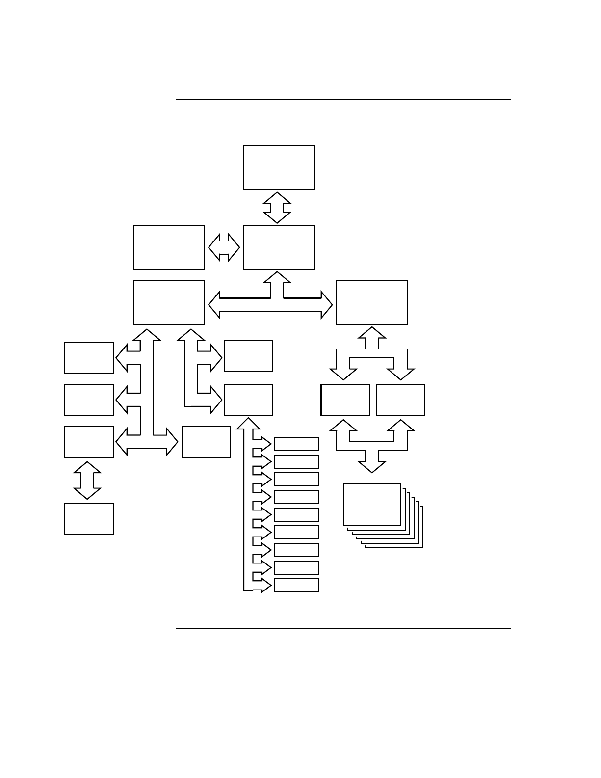
Figure 1–1 shows the major chip locations on the KA49 CPU
module.
Figure 1–1 KA49 CPU Module Components
Thick Wire Ethernet RS232 Print KBD Mouse Remote KBD/Mouse
Thin Wire Ethernet
SGEC
CEAC
Power
Connector
FLASH ROMS
DC7238
DC7238
Graph
44 QFP
Graph
84 QFP
TURBOchannel Connector
SPXg/gt Connector
LCSPX Graphics Connector
8 SIMM CONNECTORS
0A
1E
0C
1G
IF
0B
1H
0D
SQWF
NCA
Quart
SCSI
SYNC COMM Apapter
SCSI Connector
Lights & Switches
Sound
NVAXNMC
1–4
LJ-01815-TI0

Central Processor Unit
Overview
Figure 1–2 shows how, functionally, the KA49 CPU module is
divided into five major areas.
Central processing subsystem
Graphics subsystem
System support subsystem
I/O Subsystem
Memory control subsystem
Continued on next page
1–5
Central Processor Unit, Continued
Figure 1–2 KA49 CPU Module Block Diagram
G-BITS
256KB
CACHE
& TAG
NVAX
CONSOLE
ROMS
TURBO
CHANNEL
GRPHCS
ADAPT
SPXG
& GT
NCA NMC
CP2
CP1
LCSPX
SGEC
CEAC
SQWF
EDAL
NDAL
DMA RAMS
QUART
SCSI
TOY
SYNC COM
LEDS
CNFG REG
SOUND
EID ROM
DC7238
XCVR
Memory
16-128 MEG
DC7238
XCVR
SIMMS
LJ-01816-TI0
1–6
Continued on next page

Central Processor Unit,Continued
Central
Processing
Subsystem
Three Level
Cache
Architecture
The NVAX CPU (DC246) chip is the heart of the KA49 CPU
module. It executes the VAX base instruction group as defined
in the VAX Architecture Reference Manual plus the optional VAX
vector instructions and the virtual machine instructions. The
NVAX processor also supports full VAX memory management with
demand paging and a 4-gigabyte virtual address space.
The KA49 CPU module uses a three-level cache architecture to
maximize performance. The first level of cache, referred to as
the virtual instruction cache (VIC), is 2 KB in size, and is located
on the CPU chip. This cache handles instructions only (no data
references), and deals only with virtual addresses. In this way
the CPU can obtain instruction information without the need for
virtual to physical address translation, thereby decreasing latency
and improving performance.
The second level of cache, referred to as the primary cache
(Pcache), is 8 KB in size and is located on the CPU chip. This
cache implements a write-through instruction and data cache, and
helps to reduce latency on access to data and instructions that are
not found in the VIC. The Pcache uses physical addresses.
Graphics
Subsystem
The third level of cache, referred to as the backup write cache
(Bcache) is 256 KB. The Bcache is controlled by the Bcache
controller located in the CPU chip. The data and tag store
memory for this cache is located in SRAM chips on the KA49
CPU module. The Bcache uses physical addresses.
The graphics subsystem consists of either the LCSPX for low cost
graphics support or the SPXg/gt modules, which support high
performance graphics. Two connectors are provided on the module
that provide a unique interface to each.
Continued on next page
1–7

Central Processor Unit, Continued
System
Support
Subsystem
ROM Firmware
The system support subsystem handles the basic functions
required to support the console in a system environment. This
subsystem contains the firmware ROMs, the firmware ROM
controller, the configuration register, and the station address
ROM.
Resident firmware ROM is located on four chips, each 128 KB by
8 bits of programmable FLASH EPROM
1
, for a total of 512 KB of
ROM. The firmware gains control when the CPU halts.
ROM firmware provides the following services:
Board initialization
Power-up self-testing of the KA49 module
Emulation of a subset of the VAX standard console (auto
or manual bootstrap, auto or manual restart, and a simple
command language for examining or altering the state of the
processor)
Booting from supported Ethernet or SCSI devices
Configuration
Register
I/O Subsystem
Multilingual translation of key system messages
The configuration register allows the firmware and the operating
system to read KA49 configuration bits. These bits indicate which
options are present and the size of the physical memory.
The I/O subsystem contains the following:
CP-Bus adapter
SCSI mass storage interface
Ethernet interface
Optional bus adapter interface
Optional synchronous communication interface
1
A FLASH EPROM is a programmable read-only memory that uses electrical (bulk)
erasure rather than ultraviolet erasure.
Continued on next page
1–8

Central Processor Unit,Continued
Sound generator
Four asynchronous lines
Time-of-Year clock
Ethernet identification ROM
NVAX CP-Bus
Bus Adapter
Small
Computer
Systems
Interface
Ethernet
Interface
To provide buffering and connection to the I/O devices, the KA49
contains a DC243, NDAL to CDAL adapter (NCA). The NCA
provides an interface between the NVAX NDAL bus and two CPBuses where the I/O device adapters reside. As a bus adapter, the
NCA controls transactions between the higher performance NDAL
bus and the lower performance CP-Buses. Each of the NCA’s
CP-Bus ports provide a CVAX compatible peripheral bus for direct
memory access (DMA) by peripheral devices.
NCR 53C94 implements the small computer system interface
(SCSI) bus interface. It has a single port, connecting both to
devices within the BA46 system box and allowing for expansion
externally.
The Ethernet interface handles communications between the CPU
module and other nodes on the Ethernet. It is implemented with
the second generation Ethernet controller chip (SGEC) onboard
network interface. Used in connection with the module backpanel,
the SGEC allows the KA49 to connect to either a ThinWire or
standard Ethernet. It supports the Ethernet data link layer and
provides CP-Bus parity protection.
Optional
Bus Adapter
Interface
The optional bus adapter provides a translation between one of
the CP-Buses and the adapter bus. The VAXstation 4000 Model
90 has direct, transparent access to the bus adapter. The slot
appears as a region of memory in the workstation’s I/O space.
The bus adapter option can perform DMA to any location in the
memory space of the VAXstation 4000 Model 90. This DMA can be
done either directly to the physical memory of the workstation or
Continued on next page
1–9

Central Processor Unit, Continued
through a scatter/gather map that allows physically discontiguous
pages of data to appear to be contiguous to the bus adapter option.
Sound
Generator
Serial Line
Controller
Time-Of-Year
Clock
Sound output uses the DTMF tone generation capability of
the 79C30 chip. Two tone generators may be individually
programmed for frequency and amplitude; their outputs appear
summed using either the loudspeaker integral to the system
unit, or to headphones, or an external loudspeaker if plugged
in to the jack at the front of the machine. The resolution of the
frequency generators is eight bits, giving a frequency range of 8
Hz to approximately 2 kHz.
The VAXstation 4000 Model 90 system board serial line controller
handles four asynchronous serial lines. The controller consists of
the DC7085 QUART and a 64 entry FIFO RAM shared by all four
receive lines.
The time-of-year (TOY) clock consists of an MC146818BM CMOS
watch chip that keeps the date and time of day and contains 50
bytes of general purpose RAM storage. This chip includes a time
base oscillator and a lithium battery on-chip. The battery powers
the chip logic and oscillator while the system power is off.
Station
Address ROM
Memory
Control
Subsystem
1–10
A 32-byte ROM on the system board contains a unique network
address for each system. This ROM is installed in a socket so it
can be moved in the event that a system’s CPU board is replaced.
The memory control subsystem provides support for the KA49
memory subsystem. A key feature of the KA49 memory
subsystem is the use of ownership bits to maintain a sense
of ownership over each hexaword (32 bytes) of main memory.
This ownership mechanism serves the dual function of
maintaining coherency between main memory and the NVAX
Continued on next page

Central Processor Unit,Continued
cache memory, as well as providing a secure interlock mechanism
for synchronization between NVAX and the I/O devices.
The memory controller is implemented by the NVAX memory
controller chip (DC244). The NMC is an ECC protected memory
controller. The NMC controls transactions between the main
memory and the NVAX, and between main memory and any of
the I/O devices (through the NCA interface). In addition, the
NMC has a key role in maintaining main memory coherency with
the NVAX Pcache and Bcache through the use of ownership bits.
The NMC interfaces the NVAX and I/O subsystem to up to 128
MB of main memory. Main memory is comprised of one or two
sets of SIM modules. Each set contains either four 4-MB SIM
modules or four 16-MB SIM modules. The NMC controls access to
shared memory locations through the use of the ownership bits,
thereby providing a reliable interlock mechanism for memory that
is shared between the NVAX and the I/O devices.
NVAX
Data/Address
Lines
Processor
State
In order to maximize the bandwidth of the bus connecting the
CPU to the memory and I/O controllers, the NVAX chip set
(NVAX, NMC, NCA) communicates over a "pended" bus called the
NDAL. The main feature of this bus is that devices requesting
read data do not tie up the bus while waiting for the return data.
Rather, a device issues one of the "read" commands on the NDAL
and then relinquishes control of the bus to other devices. This is
so other transactions can be performed while the responder to the
first device prepares to send back the data associated with the
read request. Because of the pended nature of the bus, the NDAL
bus command set includes separate transactions for returning
data from an earlier read cycle.
The processor state consists of that portion of the state of a
process that is stored in processor registers rather than in
memory. The processor state is composed of 16 general purpose
registers (GPRs), the processor status longword (PSL), and the
internal processor registers (IPRs).
Continued on next page
1–11

Central Processor Unit, Continued
Non-privileged software can access the GPRs and the processor
status word (bits <15:00> of the PSL). The IPRs and bits <31:16>
of the PSL can only be accessed by privileged software. The
IPRs are explicitly accessible only by the move-to-processor
register (MTPR) and the move-from-processor register (MFPR)
instructions which can be executed only while running in kernel
mode.
The KA49 implements 16 GPRs, as defined in the VAX
Architecture Reference Manual. These registers are used for
temporary storage, accumulators, and base and index registers
for addressing. These registers are denoted R0 - R15. The bits
of a register are numbered from the right <0> through <31>.
Table 1–2 describes the registers.
Table 1–2 General Purpose Register Descriptions
Register Register Name Mnemonic Description
R15 Program Counter PC The PC contains the address of the next
instruction byte of the program.
R14 Stack Pointer SP The SP contains the address of the top of
the processor defined stack.
R13 Frame Pointer FP The call convention builds a data structure
on the stack called a stack frame. The FP
contains the address of the base of this data
structure.
R12 Argument Pointer AP The call convention uses a data structure
termed an argument. The AP contains the
address of the base of this data structure.
Continued on next page
1–12

Central Processor Unit,Continued
Internal
Processor
Registers
The internal processor registers (IPRs) that are implemented by
the KA49 CPU chip, and those that are required of the system
environment, are logically divided into five groups, as follows:
Normal—Those IPRs that address individual registers in the
KA49 CPU chip or system environment
Bcache Tag IPRs—The read-write block of IPRs that allow
direct access to the Bcache tags
Bcache Deallocate IPRs—The write-only block of IPRs by
which a Bcache block may be deallocated
Pcache Tag IPRs—The read-write block of IPRs that allow
direct access to the Pcache tags
Pcache Data Parity IPRs—The read-write block of IPRs that
allow direct access to the Pcache data parity bits
1–13
Interrupts and Exceptions
Overview
Nonmaskable
Interrupts
Both interrupts and exceptions divert execution from the normal
flow of control. An interrupt is caused by some activity outside the
current process and typically transfers control outside the process
(for example, an interrupt from an external hardware device). An
exception is caused by the execution of the current instruction
and is typically handled by the current process (for example, an
arithmetic overflow).
Interrupts can be divided into two classes: nonmaskable and
maskable. Nonmaskable interrupts cause a halt by way of the
hardware halt procedure. The hardware halt procedure does the
following:
Saves the PC, PSL, MAPEN<0> and a halt code in IPRs
Raises the processor IPL to 1F
Passes control to the resident firmware
The firmware dispatches the interrupt to the appropriate service
routine based on the halt code and hardware event indicators.
Nonmaskable interrupts cannot be blocked by raising the
processor IPL.
Maskable
Interrupts
1–14
Maskable interrupts cause the following:
The PC and PSL are saved.
The processor IPL is raised to the priority level of the
interrupt.
The interrupt is dispatched to the appropriate service routine
through the system control block (SCB).
Continued on next page

Interrupts and Exceptions,Continued
Interrupt
Priority Levels
Table 1–3 Interrupt Priority Levels
Priority Level Interrupt Condition SCB Offset
1F HALT_H asserted (nonmaskable) **
1E Unused
1D Bcache addressing errors 60
Table 1–3 lists KA49 interrupt conditions, associated priority
levels, and SCB offsets. Note that Table 1–3 is intended as a
quick reference, and may not include all possible causes of the
various interrupts.
Bcache uncorrectable data ECC errors on
Bcache read for a write that hits valid/owned
NVAX read timeout or read data error
on Bread for a write after the requested
quadword has arrived
Illegal length write transaction to memory or
I/O
Reserved command detected by memory or I/O
during write transaction
60
60
60
60
Pending write times out waiting for disown
write
Disown write to unowned memory location 60
Main memory NXM errors on writes 60
NDAL parity errors on writes 60
CP-Bus NXM/TIMEOUT on a write 60
1C Unused
1B Performance monitoring interrupt (internally
handled by microcode)
** These conditions generate a hardware halt procedure with a halt code of 2 (external halt).
60
Continued on next page
1–15

Interrupts and Exceptions,Continued
Table 1–3 (Continued) Interrupt Priority Levels
Priority Level Interrupt Condition SCB Offset
1A Correctable main memory errors 54
Uncorrectable main memory errors 54
Correctable O-bit memory errors 54
Pending read times out waiting for disown
write
No acknowledgment on returned read data
from NMC
NDAL Data parity errors 54
Pcache tag or data parity errors 54
VIC tag or data parity errors 54
Bcache addressing errors 54
Bcache correctable data ECC errors 54
Bcache uncorrectable data ECC errors 54
Bcache correctable tag ECC errors 54
Bcache uncorrectable data ECC errors 54
Illegal length transaction to memory or I/O
space
Reserved command to memory or I/O space 54
CP-Bus parity errors on I/O read transactions 54
CP-Bus ERR_L signal asserted by I/O device
during I/O read transaction
54
54
54
54
CP-Bus NXM/TIMEOUTS errors on I/O reads 54
19:18 Unused
17 IRQ_H[3] asserted Unused
** These conditions generate a hardware halt procedure with a halt code of 2 (external halt).
Continued on next page
1–16
 Loading...