

Digital Equipment TK50 Technical Manual
..
TK50
EK-OTKSO-
Tape
Drive
TM-001
Subsystem
Technical Manual
EK-OTKSO-
TM-001
TK50
Tape
Drive
Subsystem
Technical
Manual
Prepared
Digital
by
Educational
of
Equipment
Services
Corporation
1st
Edition,
July
1985
Copyright
All
Rights
Printed
The
in
reproduction
prohibited.
Department,
01754.
The
information
notice.
for
any
Digital
errors
CompacTape
and
Minnesota
following
The
Maynard,
Massachusetts.
DEC
DECmate
DECnet
DECUS
0
1985
Reserved.
U.S.A.
For
copy
Digital
in
Equipment
that
is
a
shared
Mining
are
DECwriter
DIGITAL
LA
MASS
PDP
by
Digital
of
this
information,
Equipment
this
may
document
appear
trademark
and
trademarks
BUS
Equipment
material,
in
contact
Corporation,
is
Corporation
in
this
of
Manufacturing
of
Digital
P/OS
Professional
Rainbow
RSTS
RSX
Corporation.
part
or
the
Maynard,
subject
assumes
document.
Digital
Company.
Equipment
whole,
Educational
to
change
no
responsibility
Equipment
Corporation,
UNIBUS
VAX
VMS
VT
Work
Processor
is
strictly
Services
Massachusetts
without
Corporation

CONTENTS
CHAPTER 1 INTRODUCTION
1.1
1.2
1.3
CHAPTER 2 DRIVE UNIT
2.1
2.2
2.2.1
2.2.2
2.3
2.4
2.5
2.5.1
2.5.2
2.6
2.6.1
2.6.2
2.6.3
2.7
2.7.1
2.7.2
2.7.3
2.7.4
2.7.4.1
2.7.4.2
2.7.4.3
2.7.5
2.7.6
2.7.7
2.7.8
2.7.9
2.7.10
2.7.11
2.7.12
2.7.13
2.7.14
2.7.15
Gene
r a 1
TK50
Drive
General
Uni t Des
Cabling
Power
Physical
Controls
Drive
Tape
to
Drive
M7546
Drive
Tape
Load
Unload
Lights
Write
Wri
Write
DC
DAC
Automatic
Read
Read
Phase
Pump Down
Pump
VCO
Pump
Data
Drive
Transport
Procedures
Board
te
Low
+12
+5
Volt
Low
Reference
Head
Amplifier
Up
Gene
Up
Detection
••••••••••••••••••••••••••••••••••••••••
Controller
THEORY
••••••••••••••••
igna
Unit
Controller
••••••••••••.
•••••••••••••
Description
Board
and
Procedures
•••••••••••
Data
Erase
Head
Circuit
Volt
Voltage
Lock
Commands
AND
SPECIFICATIONS
Drive
tions
Variations
•••••••
Indicators
Description
Chain
••••••••••
Selection
Path
Path
Gain
Select
Loop
Circuit
Circui
ra
ti
on
and
Pump Down
Unit
OF
Effect
Voltage
t
Specifications
Interface
OPERATION
••••••••••
•••••
Control
Circuitry
Circuit
Circuit
•••••
•••••••
•.•••.•••••
and
Status
Specifications
••••
Generation
Circuit
••••••
•••••
••.•••
•
••••••
•
••••
Signal
Generation
••
·
..
·
...
·
...
. .
. . .
•
~
•••••••••••
. . .
Circuit
••••
· .
.
...
. . . . . . . . .
. .
· .
· .
. . . . . . . .
·
..
. . .
....
· . .
...
1-1
1-2
1-2
2-1
2-1
2-1
2-2
2-3
2-4
2-4
2-5
2-6
2-6
2-7
2-8
2-9
2-10
2-10
2-11
2-11
2-12
2-12
2-12
2-13
2-13
2-14
2-14
2-15
2-16
2-16
2-17
2-17
2-18
2-19
2-19
iii
2.8
2.9
2.10
2.11
2.12
2.13
2.14
2.15
2.16
2.17
2.18
2.19
2.19.1
2.19.2
2.19.2.1
2.19.2.2
2.20
2.21
2.21.1
2.21.1.1
2.21.1.2
2.21.1.3
2.21.1.4
2.21.1.5
2.21.2
Tape
Link
Tape
Tape
Tape
Read/Wri
Initialization:
Wr
Differential
Signal
Serial
Basic
TK50
TK50
Hub
Arms
Cartridge
Load
Motion
i t i
ng
Contro11er-to-Drive
Drive-to-Contro1ler
Change
Dr i
Commands
Drive
Drive
Done
Enable
Dropou t Sensed
Track
Load/Run
Drive
•••••••••••••••••••••••••••••••••••••••
••••••••••••••••••••••••••••••••••••
to
te
Head
Da
ta
Interface
Controller
Controller/Drive
of
ve
De
States
State
••••••••••••
Write
Boundary.....
Error
Insertion
Beginning
11
...................................
••••••••••••••••••••••••••••••
Writing
•••••••••••••••••••••••••
Signal
Dri
tec
ted
•••••••••••
Status
State
Status
Pair
Timing
to
Drive
ve
Sta
Errors
Gate
••••••••••••
Change
••••••
of
Tape
and
Description
••••••••••••••••••••
Communications
Command
Status
te
•••••
• • • •
•••••••••
•••••••
••••••••••••
•
••••••••••
••••••
Reading
Communications
Protocol
Protocol
•••••••••••••••••
• • • • • • • •
• • • •
•••
••••
CALTRACKS
••••••••••
•••••••••••
Protocol
•••
•••••••••••
•••••
•••••
. . . . . . . . . . . .
•
••••
.......
•
•••••
•••••
•
••
•••
••••
••
.
••
..
2-20
2-20
2-20
2-20
2-21
2-21
2-21
2-23
2-26
2-26
2-29
2-29
2-30
2-30
2-30
2-30
2-31
2-32
2-32
2-33
2-33
2-33
2-33
2-33
2-34
CHAPTER 3 DRIVE UNIT REPAIR
3.1
3.2
3.2.1
3.2.2
3.2.3
3.2.4
3.2.5
3.2.6
3.2.7
3.2.8
3.2.9
3.2.10
3.2.11
3.2.12
3.2.13
3.2.14
3.2.15
3.2.16
3.2.17
3.2.18
3.2.19
3.2.20
3.2.21
3.2.22
General
Err
0 r C
Failure
Failure
General
Motor
Motor
Drive
Excessive
Failure
Cartridge
Cartridge
Move
Deceleration
Ree 1 Error
Check
Unload
8155
8155
Read
Read
Cartridge
EOT
BOT
••••••••••••••••••••••••••••••••
od
e s
••••••••••••••••••••••••••••
to
Load
to
Load
Motor
A
Failure
B
Failure
Lost
ErrQr
Byte
Memory
Timer
Head 1 Error
Head 2 Error
Sensed
Sensed
Control
Drag
to
Stop
Insert
Extract
••••••••••••••••••••
••••••••
Error
Error
Error
Error
Insert/Extract
in
in
to
Beginning
Tape
or
••••••••••••••••••••••••••
••••••••••••••••••••••••••
in
Tape
Error
••••••••••••••••••
Read/Write/Seek
Read/Write/Seek
into
Tachometer
of
Tape
Tape
Error
Error
•••••••••••••
Transport
or
Remain
••••••••
••••••
• • • • • • • • • • • • • • •
• • • • • • • • • • • • • • • • • •
Error
of
Cartridge
Failure
or
Bad
Stopped
•••••••••
•••••
•••••••.•
•
•••••
State
State
Tape
•••••••••
••••••••••
••••••
Tachometer
•••••••••••••
. . . .
. . . . . . . . .
. . . . . ....
. ....
•••
••••••••••••
••••••
•••
........
...
•
••
••
•
••
••••
3-1
3-1
3-1
3-2
3-2
3-3
3-3
3-3
3-4
3-4
3-5
3-5
3-6
3-6
3-6
3-7
3-7
3-7
3-8
3-8
3-8
3-9
3-9
3-10
iv
3.2.23
3.2.24
3.2.25
3.2.26
3.2.27
3.2.28
3.2.29
3.2.30
3.2.31
3.2.32
3.2.33
3.2.34
3.2.35
3.2.36
3.2.37
3.2.38
3.2.39
3.2.40
3.2.41
3.2.42
3.3
3.3.1
3.3.2
3.3.3
3.3.4
3.3.5
3.3
.6
3.3.7
3.3.8
3.3.9
3.3.10
Address
Address
Servo
Failure
Command
Illegal
Write
Write
No
Write
Error
Error
CALTRACKI
CALTRACK2
CALTRACK2
Tape
Top
Drive
BOT
No
Hall
No
Tachometer
Subassembly
Drive
Front
Read/Write
Tachometer
Solenoid/Interposer
Take-up
Stepper
Heat
Supply
Receiver
Overflow
Underflow
Error
in
Error
Command
Lock
Gate
Sensing
Sensing
Edge
Tape
is
Sensor
Switch
Board
Bezel
Motor
Motor
Sensor
Motor
Gate
Edge
Overheating
Assembly
Error
Error
••••••••
Tracking
Error
Signal
Error
CALTRACKI
CALTRACK2
Error
Error
Offset
Error
Tolerance
Error
Signals
Pulses
Remove/Replace
Removal
Removal
Head
Removal
Bracket
Removal
Removal
Removal
Removal
•••••
Timing
•••••
••••••••
•••••••
Error
••••••••
••••••
Present
••••••••••••••••
••••••••••••••••
•••••••••••••••
Removal
••••••
Removal
Error
Error
Procedures
Assembly
.....
.....
Removal
3-10
3-11
3-11
3-11
3-12
3-12
3-12
3-13
3-13
3-14
3-14
3-15
3-15
3-16
3-16
3-17
3-17
3-17
3-18
3-18
3-19
3-19
3-19
3-20
3-20
3-21
3-21
3-22
3-22
3-23
3-23
CHAPTER 4 TQK50
4.1
4.2
4.2.1
4.2.2
4.2.3
4.2.4
4.2.5
4.2.5.1
4.2.5.2
4.2.5.3
4.2.6
4.2.6.1
4.2.6.2
4.3
4.3.1
4.3.2
4.3.3
Gene
The
DMA
Memory
CONTROLLER
r a 1
••••••••••••••••.
80186
Power-up
Microprocessor
Memory
Peripheral
In
te
MPSC
FPLS
Non-Maskable
Operations
DMA
DMA
EPROM
Data
RAM
Microprocessor
Reset
Chip
rrup
ts
Interrupts
Interrupts
Write
Read
Transceivers
THEORY
Cycle
Select
Chip
••••••••
OF
•••••••••
Lines
Select
Interrupt
•••••
v
OPERATION
Time
Lines
...
....
4-1
4-3
4-3
4-4
4-4
4-5
4-6
4-6
4-6
4-7
4-7
4-7
4-7
4-7
4-7
4-8
4-9
4.4
4.4.1
4.4.1.1
4.4.1.2
4.4.1.3
4.4.1.4
4.4.1.5
4.4.1.6
4.4.1.7
4.4.1.8
4.4.2
4.4.2.1
4.4.2.2
4.4.2.3
4.4.2.4
4.4.2.5
4.4.2.6
4.4.2.7
4.4.2.8
4.4.2.9
4.4.3
4.4.4
4.4.5
4.4.6
4.4.7
4.4.8
4.4.9
4.5
4.5.1
4.5.1.1
4.5.1.2
4.5.1.3
4.5.2
4.5.3
4.5.4
4.5.5
4.5.5.1
4.5.5.2
4.5.6
4.6
4.6.1
4.6.2
4.7
4.7.1
4.7.2
4.7.3
4.7.4
Control
Miscellaneous
Unit
Vector
Hardware
SA
I P
Module
Unit
Revision
Q22
FPLS
Error
FPLS
Q22
DMA
Q-bus
Tape
7201
Differential
Diagnostic
Diagnostic
Miscellaneous
7201
Soft
and
Status
Control
Dri
ve
Erase
Drive
Enable
Clear
Clear
Di
Reset
Rese t LED 2 ••••••••••••••••••
SA
IP
Drive
Drive
Q-bus
Q-bus
Q-bus
Drive
Unit
Register
Reg
Bus
Bus
Data
Bus
DMA
DMA
Dri
Write
Gap
SA
IP
ag
nos
tic
LED
Number
Write
Read
Erase..................
Write
Interrupt
Interrupt
Memory
Cable
Number
Register
Revision
i s
te r •••••••••••••••••••
Starting
Number
Level
Interface
Control
Mastership
Transfer
Mastership
During
Interrupt
Bu
s Reg
Address
Address
Data
Interrupt
ve
Interface
Multi
Hardware
MPSC
Grounds
••••••
Gate
Detect
Initialization
Initialization
Mode
1 •
•••
and
Status
Initialization
Initialization
Gate
Parity
In
••••••••••••••••
•••••••.•••••••••••
Addresses/Interrupt
DIP
Switch
Switch
Logic
Logic
Phase
Q-bus
•••••••••••••••••
is
te r •••••••••••••••
and
Data
Register
Register
Logic
Protocol
Drivers
Indicators
Register
Diagnostic
••••.•••••••••••••••••••••
Register
•••••••••••••••••••••••••••
••••••••••••••••••••••••••
•••••••••
••••••••
••••••••••••••••••
Request
Request
Register
•••
Acquisition
Relinquish
DMA
Registers
•••••••••••••••••
Serial
and
•••••
Loopback
••••••••••••••••••••
Register
• • • • • • • • • • • • • • • • • • • •
••••••••••••••••
•••••••••••••••••
Register
••••••
•••••••
•••••••••
Done
Error
•••••••
• • • •
•••••••••••••••••
Pack
••••••••••••
•••••••••••
••••••••••••••••••••••••
Transfer
•••••
Receivers
"........
••••••••••
Loopback
•••••••••••••••
••••
••••••••••••••
Phase
Phase
•••••••••
••••••••••
Controller
•
••••••••
•
••••••••••
••••••••••••
.
•••••••
•
••••
••••
•••
•
•••
•
•••••••••••
Vectors
•
•••••
•••
•••
. ...
•••
•
•
••
•
••
•••
•• ••
•
•
•••••
•
••
••••••
~
••••.
....
•••••••
.....
•••
••
. .
4-9
4-9
4-10
4-10
4-10
4-11
4-11
4-11
4-12
4-12
4-12
4-12
4-12
4-13
4-13
4-13
4-13
4-13
4-13
4-13
4-13
4-14
4-14
4-16
4-16
4-20
4-20
4-21
4-21
4-22
4-23
4-24
4-24
4-24
4-25
4-26
4-26
4-26
4-26
4-27
4-27
4-29
4-30
4-30
4-30
4-31
4-32
vi
APPENDIX A
TQKSO
DETAILED
BLOCK
DIAGRAM,
TKSO
EXPLODED VIEW
APPENDIX B
INDEX
FIGURES
2-1
2-2
2-3
2-4
2-5
2-6
2-7
2-8
2-9
2-10
2-11
4-1
4-2
4-3
A-I
A-4
TKSO
SUBSYSTEM ERROR CODES
System
Desktop
Block
TK50
TK50
TK50
Physical
Recording
Signal
Signal
Frame
TQK50
Q-bus
Read
TQK50
TK50
Integrated
TK50
Diagram:
Tape
Drive
Front
Rear
View
Tape
Direction
Interface
Interface
Format
High
Level
Timing
Data
Detai
Timing
led
Exploded
AND
STATUS
TKSO
•••••••••••••••••••••••••
•••••••••••••••••••••••••••••••••••
View
Drive
Transport
••••••••••••••••••••••••••••••••
Board
•••••••••••••••••••••
••••••••••••••••••••••
•••••••••••••••••••••••••••••••••
Configuration
••••••••••••••••••••
••••••••••••••••••••••••••••
of
Timing
Timing
Data
Block
{A-P}
{Q-U}
Coming
Diagram
••••••••••••••••••
••••••••••••••••••
from
•••••••••••••••••••••••••••••••••••
•••••••••••••••••••••••••••••••
Block
View
Diagram
•••••••••••••••••••
•••••••••••••••••••••••••••••
Controller
••••••••.••••••••
••••
2-3
2-4
2-5
2-6
2-7
2-11
2-23
2-24
2-27
2-27
2-29
4-3
4-23
4-28
A-3
A-4
TABLES
1-1
2-1
2-2
2-3
2-4
2-5
2-6
2-7
4-1
4-2
4-3
4-4
4-5
4-6
B-1
B-2
B-3
8-4
B-5
B-6
B-7
B-8
TK50
States
TK50
Related
of
Signal
Lights
Differential
Signal
Interface
TK50 Command s
Non-Error
Send
Status
Drive
Miscellaneous
Common
Jumper
Address/Vector
Floating
Unit
Revision
Drive
Controller
Drive
CSR
Number
Level
Error
Internal
Error
Recoverable
Unrecoverable
Dri
ve
Flag s •••••••••••••••••••••••••••••••••••
U/Q
Port
Controller
Generic
Specific
Documentation
•••••••••••••••••••••
•••••••••••••••••••••••••••••••
Definition
Signal
Timing
•••••••••••.•••••••••••••
Pairs
••••••••••••••••••••••
••••••••••••••••••••••••
••••••••••••••••••••••••••••••••••
States
Byte
Bit
Control
Pack
Worksheet
Address
Switch
Switch
Sub-code
Code
Dri
Byte
ve
Drive
SA
Faul
•••••••••••••••••••••••••
Assignments
Register
Settings
••••••••••••••••••••
•••••••••••••••••••••••
Chart
Pack
Pack
Values
Status
•••••••••••••••••••••
Settings
•••••••••••••••••••••
••••••••••••••••••••
Byte
••••••••••••••••••••••••••
ts
•••••••••••••••••••••••
Faults
Error
SA
Error
•••••••••••••••••••••
Codes
Codes
•••••••••••••••
Bit
Assignments
•••••••••••••••
••••••••••••••••
••••••••••••••••
•••••••••••••
,.
1-3
2-9
2-25
2-26
2-28
2-31
2-32
2-33
4-10
•
4-17
4-18
4-19
4-20
4-21
B-1
B-2
B-2
B-3
B-4
B-4
B-5
B-6
vii

INTRODUCTION
CHAPTER
AND
SPECIFICATIONS
1
1.1
The
GENERAL
TK50
removable
capacity
low-end
The
the
computer
subsystem
TK50
connects
reside
entirely
MicroVAX
peripheral
PDP/II-23+.
replaceable
Future
buses
the
This
updates
other
TK50
manual
procedures
footprint
disk
may
drives,
replace
Tape
94.5M
and
Tape
the
(I
that
units
Tape
for
and
tape
or
The
than
Drive
does
is
it
the
Drive
byte
a
software
systems.
consists
Drive
drive
within·
II);
can
drive
(FRUs)
of
this
the
and
not
the
two
power-plug
may
reside
RX50
Subsystem
tape
cartridges
distribution
of
three
Controller,
to
the
the
or
it
be
plugged
unit
in
the
manual
Q-bus.
the
TQK50
contain
FRUs.
compatible
in
in
certain
is
a
components:
and
controller.
system
can
be
set
into
and
the
subsystem.
will
This
describe
version
controller
installation
Since
a
variety
configurations.
mass
storage
to
provide
capability
an
unit
up
other
controller
contains
the
TK50
with
of
the
TK50
interface
The
TK50
of
a
as
an
systems,
are
controllers
(M7546).
or
fits
the
RX
different
device.
backup
for
Digital's
Tape
It
storage
Drive,
cable
Subsystem
MicroPDP-ll
external
add-on
including
the
only
used
information
remove/replace
a
5-1/4
and
RD50
series
systems.
uses
that
may
or
the
field
with
on
inch
It
Refer
FRU
troubleshooting
MicroPDP-ll
to
the
appropriate
remove/replace
computer,
See
a TK50
Chapter
about
See
information
tape
procedures.
refer
the
Chapters
drive.
system
subsystem
to
4
for
TKSO
Subsystem
2
about
documentation
For
problem
your
Micro-II
NOTE
detailed
controller(s).
and
1-1
the
3
TKSO
for
example,
when
Pocket
information
for
detailed
streaming
installation
if
the
TK50
Service
you
is
Guide.
and
are
in
a

The
that
about
storage
is
4
by
1/2
4
medium
inch
inches
is
wide
square,
a
tape
and
cartridge
600
and
feet
is
long.
labeled
containing
The
CompacTape.
tape
a
magnetic
cartridge
tape
is
1.2
Tape
speed
Bi t densi
Data
rate
Number
Media
type
Capacity
Read/wri
spacing
Recording
Power
required
TK50 TAPE DRIVE UNIT
ty
of
tracks
te
gap
method
SPECIFICATIONS
75
inches
6667
500
bits
Kbits/second;
per
per
22
Single
131
megabytes
0.3
MFM,
reel,
megabytes
inches
bit
formatted
serial
recording
+5
1
.4
+12
2.4
Vdc,
amps
Vdc,
amps
1.2
(max)
2.0
(max)
second
inch
1/2
amps
amps
(in/s)
(bits/s)
45
Kbytes/second
inch,
600
unformatted,
data,
(typ),
(typ),
feet
long
94.5
serpentine
1.3
Interface
Connector
Cable
type
Receiver
Driver
DRIVE
type
type
type
type
TO
CONTROLLER INTERFACE
Differential
and
26-pin
angle
26-wire
max
AM
AM
rece i vers
header;
length
26LS32,
26LS3l,
1-2
SPECIFICATIONS
using
flat
flat
ribbon,
PN
ribbon;
10
ft
12-16832-02
differential
differential
RS-422
polarized;
PN
17-00034-02;
drivers
right
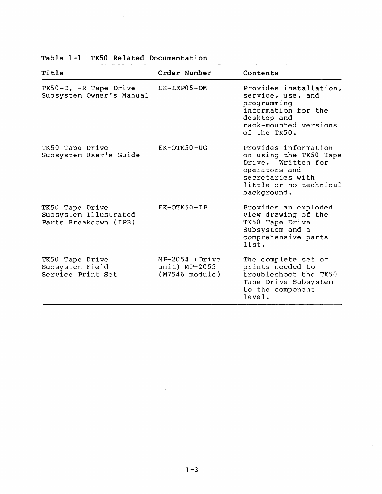
Table
1-1
TK50
Related
Documentation
Title
TK50-D,
Subsystem
TK50
Tape
Subsystem
TK50
Tape
Subsystem
Parts
Breakdown
-R
Tape
Owner's
Drive
User's
Drive
Illustrated
Drive
Manual
Guide
(IPB)
Order
Number
EK-LEP05-0M
EK-OTK50-UG
EK-OTK50-IP
Contents
Provides
service,
installation,
use,
programming
information
desktop
and
rack-mounted
of
the
TK50.
Provides
on
using
Drive.
operators
information
the
Written
and
secretaries
little
or
no
background.
Provides
view
TK50
Subsystem
an
drawing
Tape
Drive
and
comprehensive
list.
and
for
the
versions
TKSO
for
with
technical
exploded
of
the
a
parts
Tape
TK50
Tape
Subsystem
Service
Drive
Field
Print
Set
MP-20S4
uni
t)
MP-20
(M7546
(Dri
55
module)
ve
The
complete
prints
needed
troubleshoot
Tape
to
Drive
the
component
level.
set
of
to
the
TKSO
Subsystem
1-3

THEORY
CHAPTER 2
DRIVE
OF
OPERATION
UNIT
2.1
This
TK50
chapter
Tape
discussed
Use
the
you
understand
Print
Set
drawings
This
chapter
Drive
theory
and
timing,
the
basic
Chapter
a
subassembly
2.2
This
TK50
section
Tape
GENERAL
provides
Drive.
in
block
takes
in
succeeding
this
The
diagrams
the
text.
precedence
book.
controller(s)
describes
Unit
is
interact
more
command
during
specific
summary
drive/controller
3
provides
that
the
failed
UNIT DESIGNATIONS
lists
Drive
and
Subsystem
theory
chapters.
and
mechanical
For
over
how
the
operation.
information
and
communications
information
in
the
describes
is
available.
of
operation
to
which
drawings
troubleshooting,
any
block
various
including
explanation,
necessary
drive.
the
unit
information
the
referenced
diagrams
components
Following
and
protocol.
to
remove
variations
drive
the
signal
a
about
connects
to
Field
or
in
the
Service
mechanical
the
overview
definition
discussion
and
replace
in
which
the
is
help
TK50
of
the
2.2.1
Drive
Unit
TK50
TK50-AA
TK50-AX
TK50-D
TK50-R
Variations
Plain
Single
Single
Desktop
version.
Rackmount
version.
drive,
unit
unit
version
ordered
in
packaging
in
packaging,
version
2-1
of
of
with
TK50
TK50
no
with
no
--
system.
tape
tape
external
--
external
cartridge.
cartridge.
drive
drive
2.2.2
M7546
Controller
TQK50-AB
TQK50-PB
17-00484-01
TQK50-AA
TQK50-BA
This
variation
enclosure
accommodates
one
TK50
Use
MicroVAX
This
the
drive.
this
system
kit
controller
system.
Use
this
This
interface
50-pin
cable.
kit
2.75
cable
"D"
This
subsystem.
Controller
with
BA23
Controller
is
and
the
kit
is
the
when
meter
subminiature
cable
and
specific
in
BAl23
the
an
external
MSCP
when
in
a BA23
same
cable
configuring
(9
is
a
comes
cable
access
cabinet,
controller
Q-bus.
configuring
enclosure.
as
the
accommodates
foot)
50-pin
female
with
in
BA23
door.
30
and
TK50-D,
One
controller
a
one
a
above,
PDP-ll/23+.
cable
-R
MicroPDP-ll
for
drive,
except
a
PDP-ll/23+
host-to-external-drive
subminiature
male
shielded,
the
cabinet,
inch
TK50-D,
30
cable.
inch
a
BA23
and
handles
or
that
to
molded
TK50-R
cable
a
TQK50-BB
TQK50-CB
TQK50-RB
The
TK50
separate
controller.
(BA23
would
enclosure)
order
1.
2.
3.
Controller
with
Controller
and
panel
Controller
no
I/O
I/O
panel
only.
Tape
Drive
pieces:
For
example,
and
the
following
TK50-D
-17-00484-01
TQK50-AB
I/O
panel
external
insert.
panel,
insert
Subsystem
the
want
Desktop,
--
--
Controller
in
BA123
insert.
in
cabinet
drive.
in
non-FCC
120
drive
if
to
parts.
external
External
and
external
mount
Also,
compliant
inch
on
cable
cabinet
must
unit
itself
customers
add
an
external
version
drive-to-system
and
internal
BA23
36
rails.
always
drive,
with
inch
Q-bus
with
be
and,
21
H3490
cable
enclosure
bracket
For
Field
ordered
separately,
own a MicroVAX I
TK50
of
Subsystem,
drive
cable.
cable.
inch
I/O
with
to
cable
panel
I/O
with
mount
upgrade
in
two
the
system
they
2-2
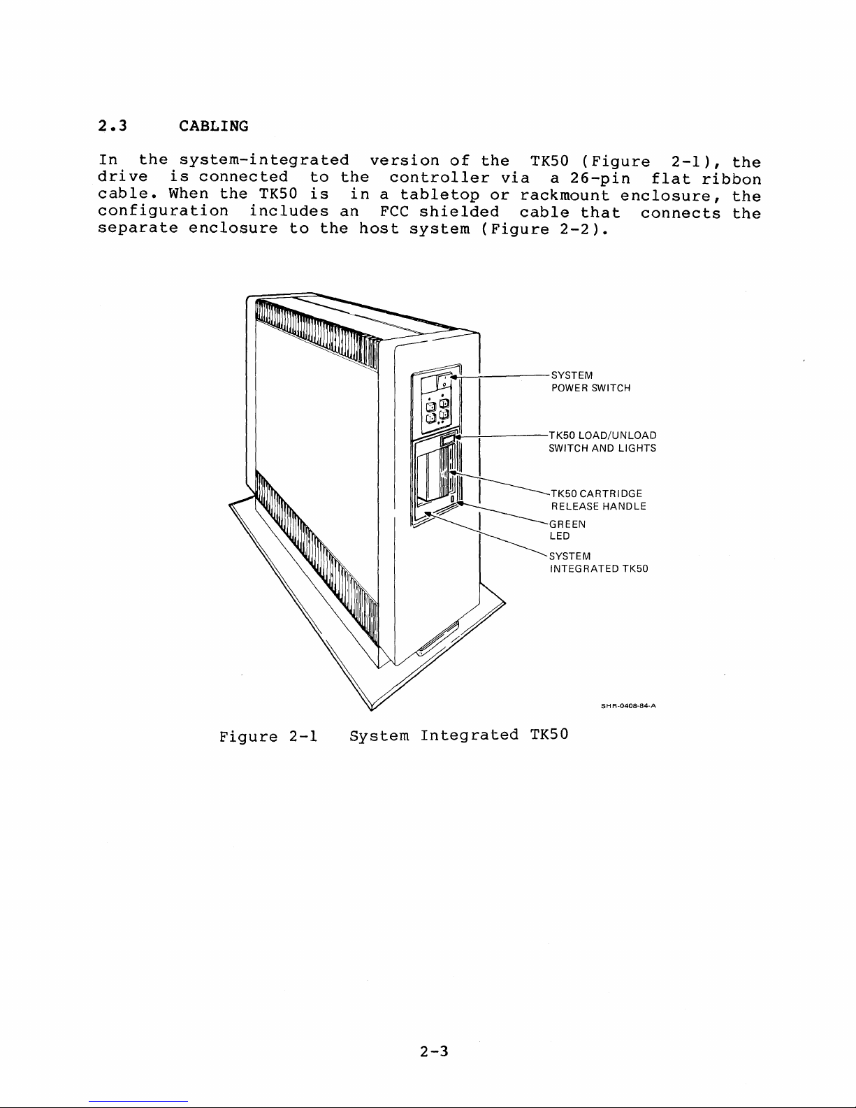
2.3
In
drive
cable.
CABLING
the
system-integrated
is
When
configuration
separate
enclosure
connected
the
TK50
includes
to
to
is
the
the
in
an
version
controller
a
FCC
host
of
tabletop
shielded
system
the
via
or
rackmount
cable
(Figure
TK50
a
(Figure
26-pin
that
2-2).
2-1),
flat
enclosure,
connects
the
ribbon
the
the
Figure
2-1
System
Integrated
2-3
TK50
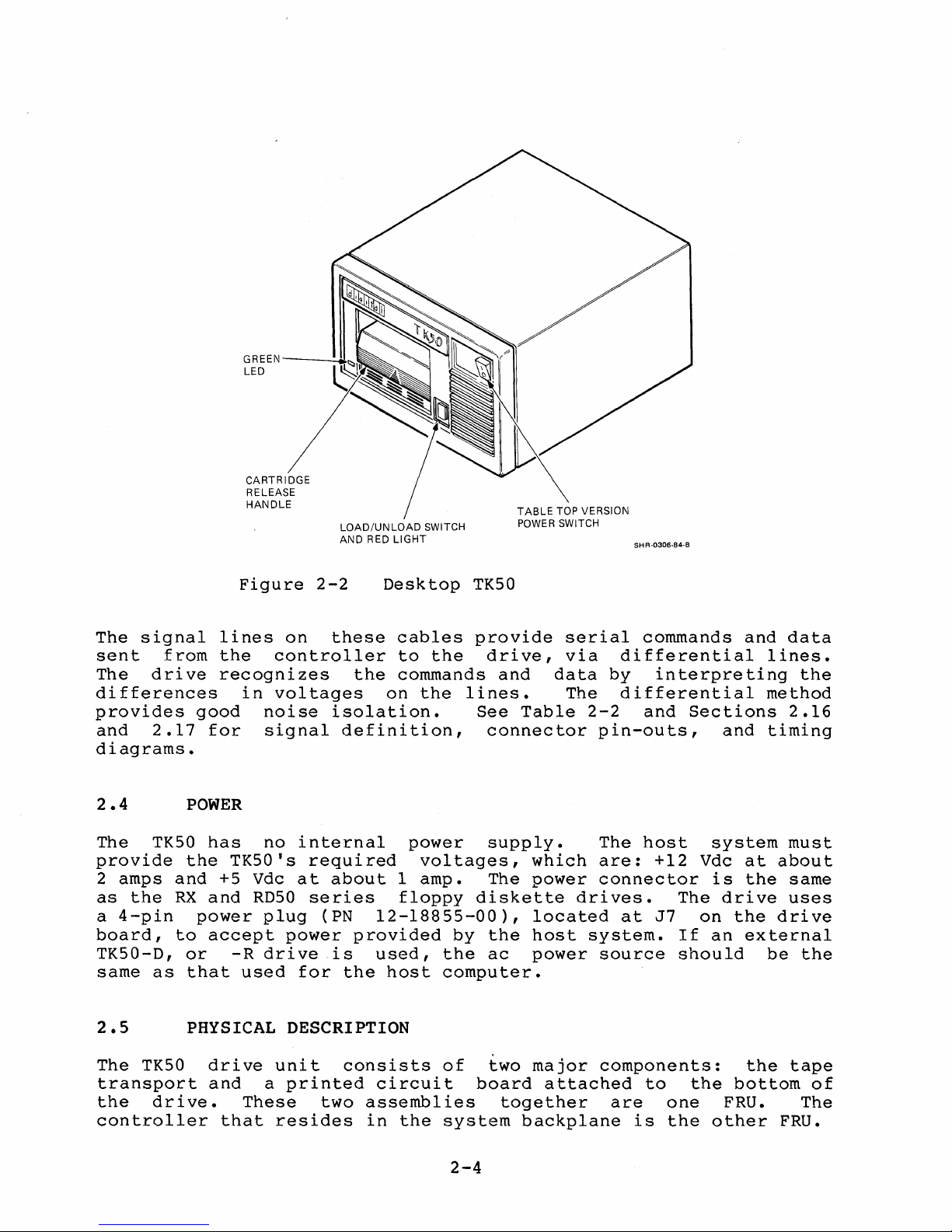
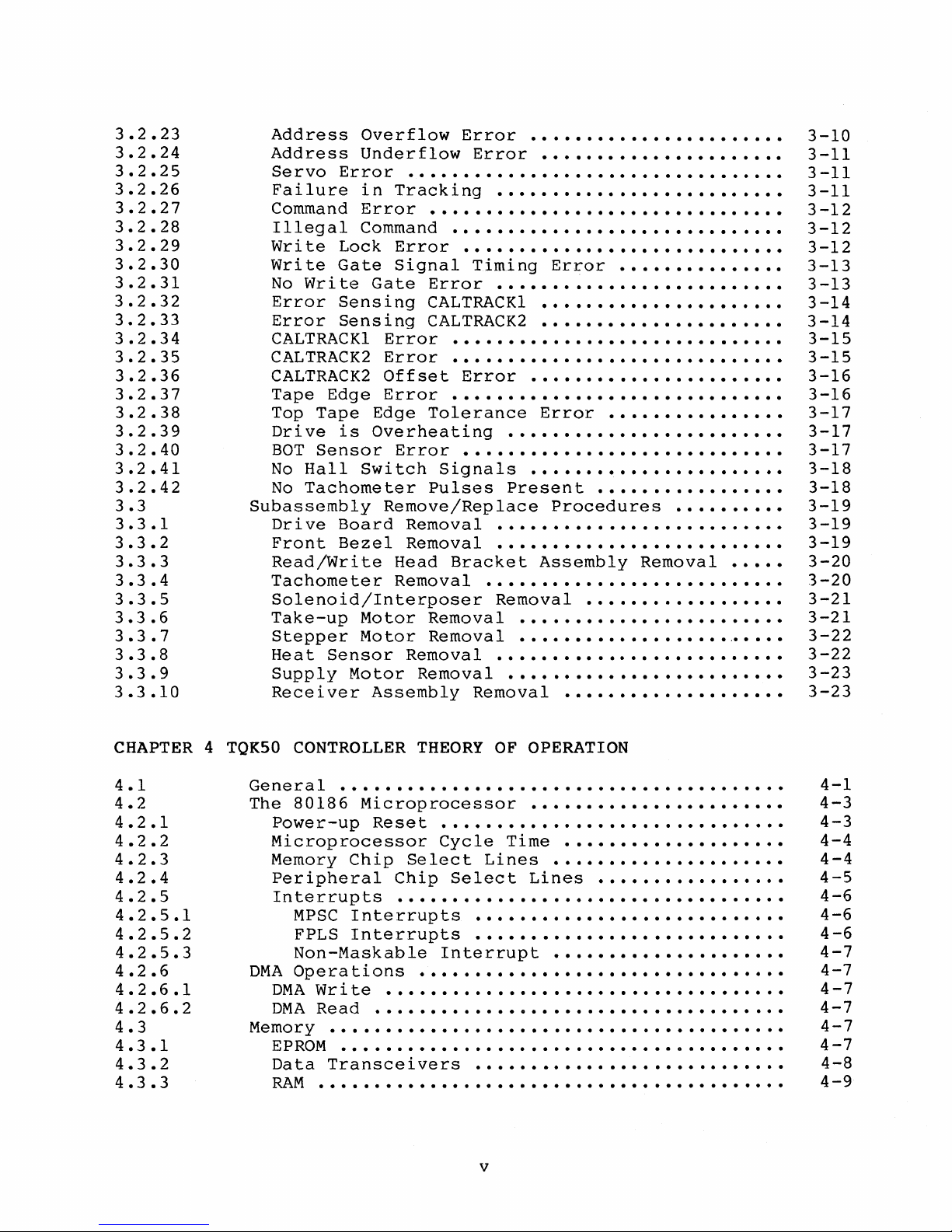
GREEN----...ioI..
LED
CARTRIDGE
RELEASE
HANDLE
LOAD/UNLOAD
AND RED LIGHT
SWITCH
TABLE
POWER
TOP
VERSION
SWITCH
SHR-0306-84-B
The
signal
sent
The
from
drive
differences
provides
and
2.17
diagrams.
2.4
The
provide
2
as
a
board,
TK50-D,
same
TK50
amps
the
4-pin
as
and
RX
to
2.5
Figure
lines
the
recognizes
in
good
for
POWER
has
the
TK50's
+5 Vdc
and
RD50
power
accept
or
-R
that
used
PHYSICAL
2-2
on
these
controller
the
voltages
noise
signal
no
isolation.
definition,
internal
required
at
about
series
plug
drive
(PN
power
for
provided
is
the
DESCRIPTION
Desktop
cables
to
TK50
provide
the
commands
on
the
lines.
See
power
voltages,
1
amp.
floppy
diskette
12-18855-00),
by
used,
host
the
computer.
drive,
and
data
Table
connector
supply.
which
The
power
located
the
host
ac
power
serial
via
The
2-2
pin-outs,
The
are:
connector
drives.
system.
source
commands
differential
by
interpreting
differential
and
host
+12
The
at
J7
If
should
and
Sections
and
system
Vdc
at
is
the
drive
on
the
an
external
data
lines.
the
method
2.16
timing
must
about
same
uses
drive
be
the
The
TK50
transport
the
drive.
controller
drive
and
These
that
unit
a
printed
resides
consists
two
of
circuit
assemblies
in
the
system
2-4
two
board
together
major
attached
backplane
components:
to
the
are
is
one
the
the
bottom
FRU.
other
tape
of
The
FRU.
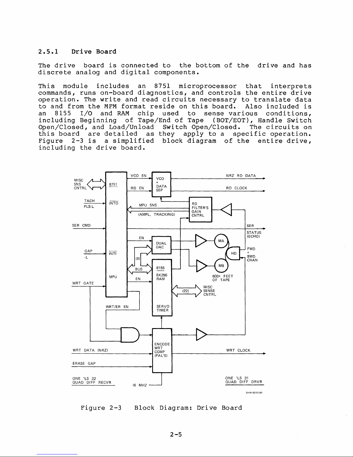
2.5.1
The
drive
discrete
Drive
board
analog
Board
is
and
connected
digital
to
the
components.
bottom
of
the
drive
and
has
This
module
commands,
operation.
to
and
from
an
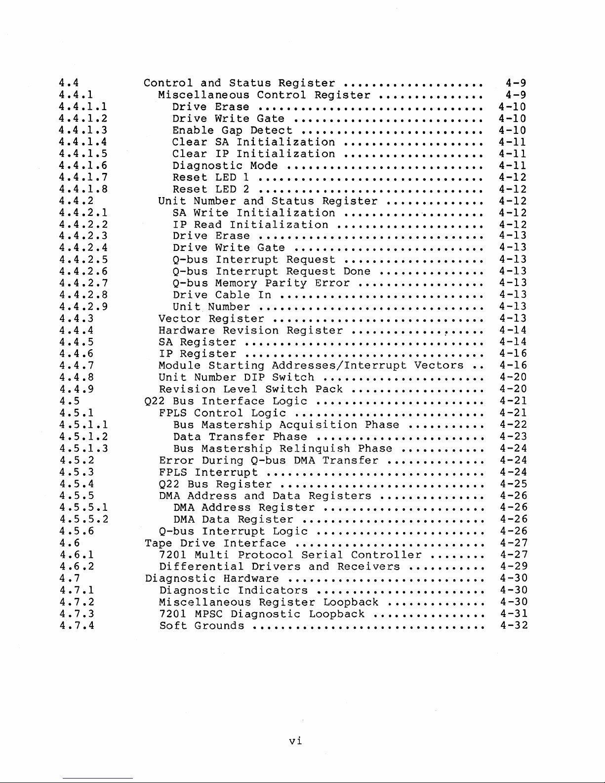
8155
including
Open/Closed,
this
Figure
board
2-3
including
MISC
SNS
CNTRL
SER CMD
WRT
includes
runs
I/O
The
the
on-board
write
MFM
and
Beginning
and
Load/Unload
are
detailed
is
a
the
drive
8751
TACH
PLS-L
GAP
-L
GATE
INTO
INTI
MPU
an
diagnostics,
and
read
format
RAM
chip
of
Tape/End
simplified
board.
VCO
EN
RD
EN
MPU SNS
(AMPL,
EN
EN
8751
reside
as
they
VCO
+
DATA
SEP
TRACKING)
DUAL
DAC
8155
8X256
RAM
microprocessor
and
circuits
on
this
used
Switch
to
of
Tape (BOT/EOT),
Open/Closed.
apply
block
diagram
controls
necessary
board.
sense
to
a
of
NRZ
RD
600+
FEET
OF TAPE
MISC
SENSE
CNTRL
that
the
to
Also
various
The
specific
the
RD
DATA
CLOCK
SER
STATUS
(ECHO)
FWD
+
BWD
CHAN
interprets
entire
translate
included
conditions,
Handle
circuits
operation.
entire
•
drive
data
is
Switch
on
drive,
WRT/ER
WRT
DATA
-----------~
ERASE
ONE
QUAD
(NRZ)
GAP
'LS
32
DIFF
RECVR
Figure
2-3
EN
16
MHZ
Block
SERVO
TIMER
ENCODE
WRT
COMP
(PAL'S)
Diagram:
2-5
Drive
WRT
CLOCK
ONE
'LS
QUAD
Board
DIFF
31
SH
DRVR
R-0212-85
2.5.2
Tape
Transport
(Figure
2-4)
The
tape
drive
electromechanical
functions;
These
stepper
serves,
inserted)
feedback
components
that
motor;
effectively,
and
to
the
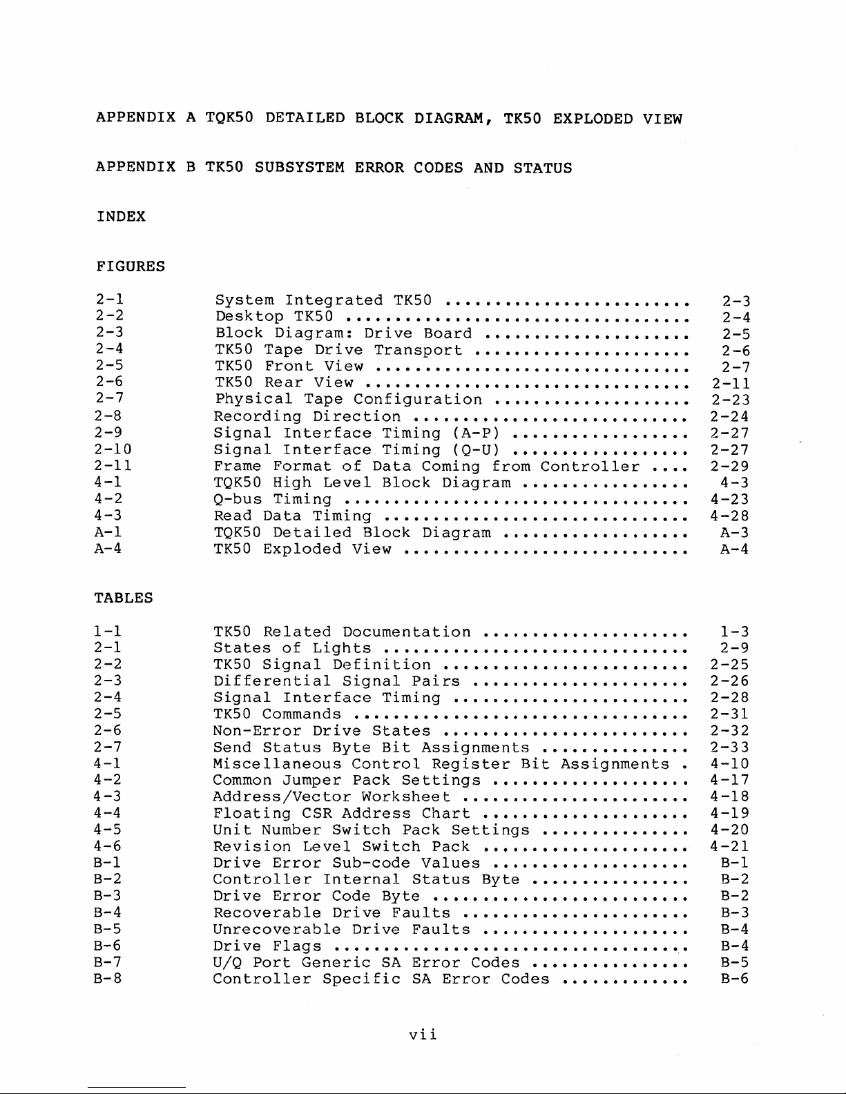
TACHOMETER
ASSEMBLY
BRACKET
HEAD
ASSEMBLY
&
transport
components
is,
include:
the
take-up
its
reel
8751
LEADER,
EXTERNAL
SHIELD
ASSEMBLY
encompasses
that
to
read
and
the
reel
as
the
supply
motor;
and
microprocessor
TAKE-UP
allow
write
magnetic
and
its
reel
the
regarding
REEL,
the
the
TK50
data
read/write
motor;
when
the
a
tachometer,
tape
TAKE-UP
mechanical
to
to
magnetic
tape
tape
which
speed.
perform
head
hub
cartridge
and
its
tape.
and
its
(which
provides
is
Figure
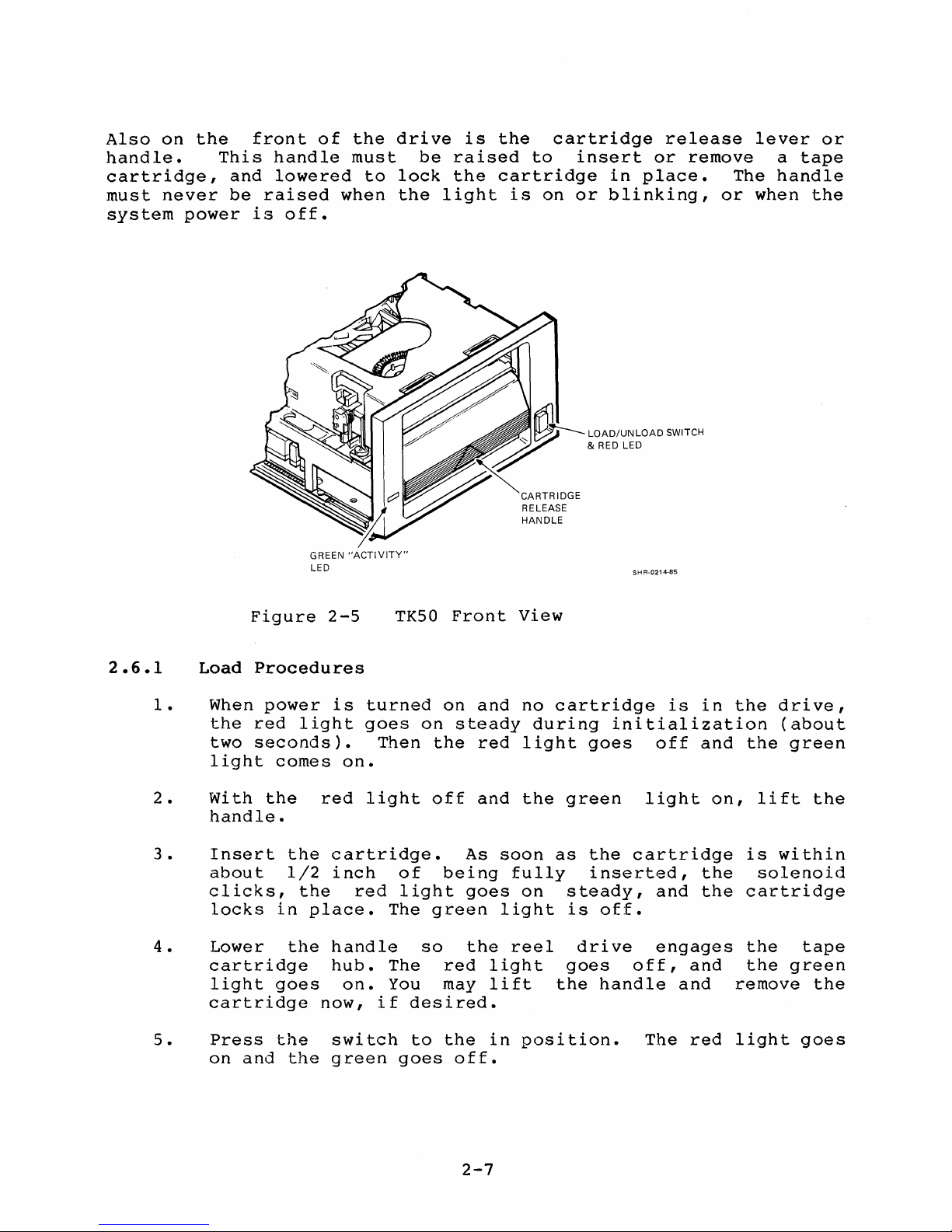
2.6
On
the
and
LED
cartridge
tape
leaders
other
Beginning
rewinding
seat
for
in
2-4
CONTROLS
front
indicator
is
the
of
is
in
operation.
together
part
of
Tape
to
BOT,
cartridge
TK50
DRIVE
MODULE
TK50
AND
the
(Figure
place,
(one
of
(BOT)
then
INSULATOR
ASSMEBLY
Tape
INDICATORS
TK50
the
Drive
2-5).
the
Loading
is
on
drive),
indicator.
unbuckling
for
removal.
Drive
is
Transport
a
combination
When
Load/Unload
the
the
beginning
then
the
2-6
power
switch
tape
involves
of
bringing
Unloading
two
leaders
BEZEL
ASSEMBLY
Load/Unload
is
applied
is
used
the
the
the
coupling
tape
tape
tape·
so
the
SH
and
to
R·0213·85
switch
a
tape
load
the
two
and
the
to
the
involves
tape
can
Also
on
handle.
cartridge,
must
never
system
the
This
power
and
be
front
handle
lowered
raised
is
off.
of
the
must
to
when
drive
be
lock
the
is
raised
the
light
the
cartridge
to
cartridge
is
on
insert
in
or
blinking,
release
or
place.
remove
The
or
lever
a
handle
when
or
tape
the
2.6.1
1.
2.
3.
4 •
5.
Figure
Load
When
the
two
light
With
handle.
Insert
about
clicks,
locks
Lower
cartridge
light
cartridge
Press
on
and
2-5
Procedures
power
red
is
light
seconds).
comes
the
the
1/2
red
cartridge.
inch
the
in
place.
the
handle
hub.
goes
now,
the
the
switch
green
on.
red
on.
TK50
turned
goes
Then
light
of
light
The
The
You
if
goes
Front
on
on
steady
the
off
being
green
so
red
may
desired.
to
the
off.
and
red
and
As
goes
the
light
lift
in
View
no
during
light
the
soon
fully
on
light
reel
position.
cartridge
initialization
goes
green
as
the
inserted,
steady,
is
off.
drive
goes
the
handle
is
off
light
cartridge
and
engages
off,
and
and
The
red
in
and
on,
the
the
the
drive,
(about
the
lift
is
within
solenoid
cartridge
the
the
remove
light
green
the
tape
green
the
goes
2-7
6.
Tape
loads
successfully
is
on
steady.
a
command
the
correct
blinking.
to
loaded
to
BOT
During
read
part
(beginning
and
waiting
the
or
write,
of
the
time
of
tape).
at
the
including
tape,
BOT,
drive
the
When
the
is
the
green
the
tape
green
responding
time
to
light
is
light
to
seek
is
2.6.2
1.
2.
3.
4.
5.
6.
Unload
Red
Red
together)
rewind
lights
Red
continues
When
the
Raise
easily
Lower
that
Procedures
light
light
operation
blink
light
the
red
light
the
grasp
the
there
Do
not
cartridge
remove
down.
is
on.
and
as
in
green
the
either
stays
rewinding
tape
is
goes
handle.
and
handle.
is
power
power
is
the
Press
the
light
tape
can
also
case.
on
and
to
the
completely
off.
The
cartridge
remove
The
to
the
NOTE
down
the
still
cartridge
switch
is
be
green
unload
Then
it.
green
drive.
TK50
in
the
both
being
initiated
light
rewound
the
light
when
drive.
before
to
the
blink
rewound
goes
position.
green
comes
is
the
powering
out
(slowly,
from
off
into
light
out
still
tape
Always
position.
to
BOT.
software.
as
the
cartridge,
comes
far
enough
on
but
the
to
not
This
The
tape
on.
to
show
2-8
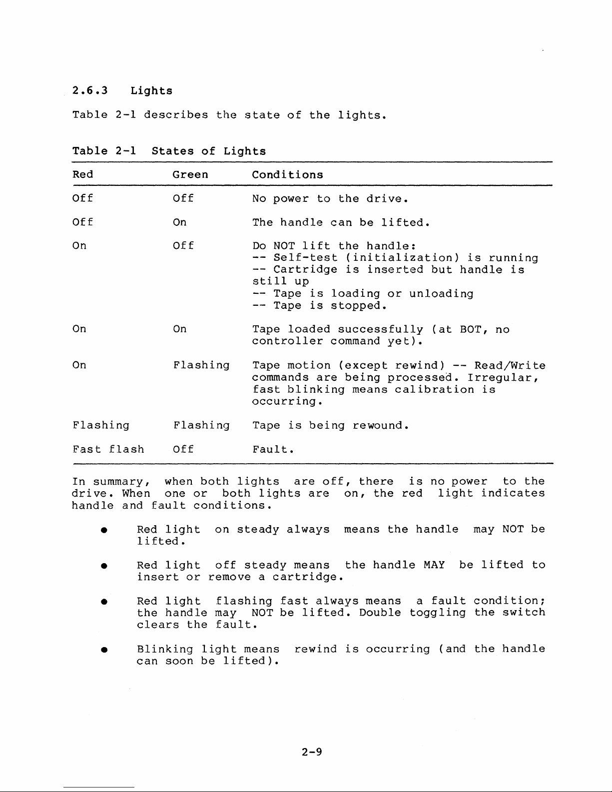
2.6.3
Lights
Table
Table
Red
Off
Off
On
On
On
2-1
2-1
describes
States
Green
Off
On
Off
On
Flashing
of
the
Lights
state
of
Conditions
No
power
The
handle
Do
NOT
Self-test
Cartridge
still
--
Tape
--
Tape
Tape
controller
Tape
motion
commands
fast
blinking
occurring.
the
to
lift
up
is
is
loaded
are
lights.
the
drive.
can
be
lifted.
the
handle:
(initialization)
is
inserted
loading
stopped.
successfully
command
(except
being
means
but
or
unloading
(at
yet).
rewind)
processed.
calibration
is
handle
BOT,
--
Read/Write
Irregular,
is
running
is
no
Flashing
Fast
In
flash
summary,
drive.
handle
•
•
•
•
When
and
Red
lifted.
Red
insert
Red
the
clears
Blinking
can
when
one
fault
light
light
light
handle
soon
Flashing
Off
both
or
conditions.
or
remove
the
light
be
lights
both
on
steady
off
steady
flashing
may
fault.
means
lifted).
Tape
Fault.
lights
a
cartridge.
NOT
is
are
always
means
fast
be
lifted.
rewind
being
off,
are
always
rewound.
there
on,
the
means
the
handle
means
Double
is
occurring
red
the
is
no
light
handle
MAY
a
fault
toggling
(and
power
may
be
condition;
the
the
to
indicates
NOT
lifted
switch
handle
the
be
to
2-9
The
green
light
indicates
tape
and
power
conditions.
2.7
Refer
Print
•
•
•
DRIVE
to
Set
Green
1.
light
Power
insert
off).
2.
Tape
Green
used
tape
Green
light
(it
is
light
loading
motion.
1.
Calibration
2.
Read/write
3.
The
tape
BOARD
the
drive
(MP-2054-CS)
on
steady
is
on
and
or
remove
has
loaded
off
steady
is
stopped,
or
blinking
is
activities
is
rewinding
DESCRIPTION
board
while
means
the
handle
a
cartridge
properly
means
initialization
unloading,
always
occurring.
schematics
reading
two
means
are
to
this
may
(if
the
or
being
BOT.
in
things.
be
(if
red
tape
is
fault).
that
performed.
the
section.
lifted
red
light
light
is
not
occurring,
tape
TK50's
to
is
being
is
Field
is
on).
in
Service
In
the
following
is
followed
and
location
Print
Set
B8.
2.7.1
Write
signal
2-6).
receiver
output
data
Write
data
cable
It
at
of
and
Programmable
through
clock
the
is
oscillator.
data
accepts
rate.
this
in
parentheses
zone.
MP-2054,
Data
comes
on
into
26-pin
connects
E13
(1-B8).
the
differential
outputs
Array
shift
divided
The
The
clock
logic
For
Circuit
Chain
the
to
a
Logic
register
down
500
KHz
M7546
also,
description,
by
example,
Schematic
drive's
connector
pins
The
receiver
five-bit
(PAL)
by
by
the
clock
controller
and
must
the
E13
one
shift
parallel
at
the
is
circuit
(1-B8)
logic
Jl'
and
E9
PAL
the
that
keep
the
component
(CS)
board
(PN
two
register
is
connected)
(1-B5).
500
KHz
from
write
is
up
being
schematic
is
in
Field
sheet
via
1,
the
12-16832-01)
of
the
at
E4
data
pattern
The
data
clock.
the
24.0
pulse
in
the
with
it.
described
sheet
Maintenance
location
differential
(see
differential
(to
which
accepts
into
is
The
MHz
rate,
host
number
zone
Figure
the
serial
the
clocked
500
KHz
crystal
or
write
computer
~
~
.... -..................
........................
:wJr.rnn
~~~
W@J]j
"'''-''-'-DO
II
.
The
PAL
register
This
PAL
translate
The
signal
at
E19
of
the
toggling
the
write
of
the
transitions
2.7.2
The
PAL
WR
ERASE
pulses.
heads.
with
the
no
write
encoding
1iiiiiiiiii~~~~iiiiiii7
Figure
at
E9
at
E4
performs
data
WR
(2-D4),
flip-flop
of
E19,
driver
selected
necessary
Write
at
E9
L
(write
Write
Therefore,
data.
erase
and
resumes
J1
(26 - PIN
accepts
(1-B6),
to
MFM
PLS L
which
switches
in
circuit,
write
Erase
controls
current,
an
This
signal
SIGNAL
2-6
CONNECTOR)
TK50
the
and
the
precompensation
format.
is
connected
is
set
conjunction
pumps
head.
to
write
the
erase)
however,
erase
function
is
the
generation
Rear
five
from
up
as
each
current
This
data
write
is
asserted,
function
is
released,
those
to
a
time
with
erase
is
used
View
parallel
bits
pin
toggle
WR
the
alternately
toggle
to
tape.
function.
still
is
performed;
to
write
the
of
write
POWER CONNECTOR
bits
generates
and
3
encoding
of
the
flip-flop.
PLS L
7426
at
action
the
PAL
flowing
gaps
PAL
goes
pulses.
SH
R-0215-85
from
74S74
goes
E23
into
results
When
shuts
that
on
(J71
high.
to
tape.
back
the
WR
PLS
needed
flip-flop
The
(2-D4)
each
in
the
signal
off
the
is,
to
shift
L.
to
sense
The
and
coil
the
write
write
write
When
MFM
2.7.3
The
WR
HD
data
write
2 SEL
in
Write
heads
the
Head
are
(E23
pins
forward
Selection
selected
8,
9,
direction,
by
10;
the
pins
head
2-11
signals
11,
two
in
12,
WR
the
HD
13).
reverse
I SEL
Head
or
one
writes
direction.
With
to
0,
Current
coil,
13,
flip-flop
of
application
write
the
pin
which
14),
15
10
through
data
signals
or
pin
grounds
is
then
the
or
E30
E19
milliamps
of
to
magnetic
HD
1(2)
13
the
alternately
transistor
(pins
switches.
to
the
current
of
5,
SEL H
the
centertap
6,
This
each
tape.
asserted
7426
applied
pairs
7
and
provides
write
results
at
1,
E23.
of
to
at
2,
head
in
high,
the
each
E30
3),
a
the
a
E23
then
selected
side
(pins
each
constant
coil.
transitions
logic
of
8,
time
1
outputs
write
the
9,
the
current
The
is
applied
a
write
10
and
sense
source
alternate
needed
logic
head.
head
12,
of
to
2.7.4
The
DC
+12
V
dropping
functions
resets
write
2.7.4.1
acceptable
If
of
turning
drops,
A
hysteresis.
discharges,
it
oscillating
voltage
DCLOW
current
I-AI)
the
that
330
off
voltage
asserting
nf
signal
DC
Low
Low
circuit
of
the
8751
+12
Volt
level
is
turned
transistor,
on
E6
capacitor
When
dumping
harder.
if
drops.
is
Circuit
senses
below
the
tape
microprocessor
circuitry.
Path
(about
on.
drops
(6,
7,
the
DCLOW
some
The
there
The
of
a
(Sheet
their
drive.
--
As
10
lower
E6
(1,
8).
signal
(C47)
goes
charge
hysteresis
is
hysteresis,
long
enough
2)
a
low
acceptable
It
at
long
V)
the
than
15,
When
DC
LOW
provides
to
back
noise
duration.
voltage
shuts
E1
as
+12
transistor
the
base-emitter
16)
E6
(6,
L.
positive
a
logic
prevents
at
its
then,
levels)
(1-D6),
volts
turns
7,
to
pin
is
condition
down
base
at
8)
level
16
to
the
doesn't
off.
turns
the
(pin
make
(either
and
shuts
motor
and
E6
(pins
junction
Pin
on,
feedback
0,
the
of
E6,
transistor
16)
sure
down
current,
disables
go
below
1,
voltage
1
its
and
capacitor
and
turning
when
that
+5
the
the
15,
rises,
pin
some
from
the
the
or
an
16
7
Also
(pins
asserted.
the
until
2.7.4.2
same
The
(12,
and
(1,
as
E6
2,
reset
+5
transistor
+5 V
13,
E6
pin
15,
16)
3,
The
line
volts
+ 5
low
14).
pin
4)
Volt
circuit
11
and
1
rises
1
MF
to
has
pair
If
reach
E6
is
the
ramped
Path
+5
(6,
(pulled
turned
capacitor
8751
up
--
The
as
+12
consists
V
drops
about
7,
8).
up
by
on
and
at
C3
microprocessor
completely
signal
V
(E6).
essentially
lower
3.9
V.
This
2-12
R19
the
(1-A3)
and
DCLOW
than
to
+5
reset
discharges.
asserted
cleanly.
is
asserted
of
E6
about
asserts
V),
signal
(9,
4.6
DCLOW
transistor
RST H
on
through
10,
11)
V,
E6
through
E6
is
C3
holds
power-up
the
and
E6
pin
12,
E6
2.7.4.3
a
low
(2-D4).
to
assert
PAL
reference
circuit
shuts
on
at
Low
the
When
pin
off
is
E23
Voltage
set
the
9
of
the
shut
pins
input
set
the
1
down.
13
Effect
input
PAL
MHz
DCLOW
and
of
9.
-the
is
at
E9.
clock.
also
When
74874
asserted,
When
In
disables
DCLOW
flip-flop
this
this
is
it
asserted,
causes
pin
way
the
at
is
the
write
it
E19,
the
flip-flop
asserted,
-1.25
head
places
pin
the
volt
select
10
When
-1.25
motors.
current
2.7.5
This
and
The
originates
When
(plus
signal
Cll.
and
voltage
The
The
multiplying
to
microprocessor.
numbers
programmable
op-amps
the
larger
the
PAL
reference
Regardless
is
DAe
section
how
minus
Cll
minus
microprocessor
the
voltage
diode
the
the
reference
1
comes
When
holds
source
DAC
into
at
or
smaller
shuts
shut
down
Reference
explains
DACs
at
pin
MHz
signal
on
down,
the
1
the
at
voltage
at
D4
Digital-to-Analog
at
it,
current
E16
(3-03)
off
voltage
of
when
Voltage
how
use
that
voltage
17
of
rises
pin
1,
C6
MHz
charge.
pin
1
source
develops
E8
The
micropocessor
using
controls
can
numbers
the
what
used
the
1
else
minus
Generation
the
minus
voltage
is
the
PAL
to
minus
discharges,
signal
of
are
source.
speed
goes
This
Cll.
goes
a
Converter
the
the
up
into
MHz
clock,
by
the
happens
voltage
reference
to
energize
generated
at
E9
about
voltage
and,
up
provides
to
the
-1.25
data
selects
data
the
or
the
bus.
Its
speed
slow
DAC.
DACs
at
Circuit
from
(1-B5).
4 V,
again,
output
it
on
pin
through
a
lK
reference
at
bus
of
down
it
also
which
this
reference
voltage
the
the
charges
2).
D5
minus
resistor
E8
(3-D5).
bits
the
The
current
the
reel
the
shuts
drive
point,
reel
1
MHz
When
diode
is
reve~se
2.1
at
voltage
from
DAC,
DAC
motors.
motors
off
the
the
is
removed.
is
generated
motors.
clock
capacitor
the
D5,
charges
biased
V
constant
R3
(3-D6).
for
The
the
then
acts
through
by
writes
like
writing
the
reel
motor
that
C6
1
MHz
the
inputs
8751
the
Thus
a
The
(control
are
motors'
B
reference
signals
actually
are
A
for
printed
current
to
Control
motor
connected
circuit
return
the
DAC.
A
A
and
and
to
board.
signals
Control
control
three
The
2-13
B
B
darlington
signals
from
drive
for
the
the
motor
transistors
Feedback
motors
B).
two
A
that
reel
These
and
provide
motors
signals
on
the
Feedback
a
2.7.6
The
4024
(R31
--
existence
only
2),
the
The
to
then
desired
gain
applied
(2-C8)
through
transistors
developing
averaged
The
intensity
by
the
op-amp.
resistors
and
03
are
the
gain
counter
is
translated
op-amp
the
at
at
appropriate
the
op-amp.
Automatic
at
E12
R36)
set
make
of
the
up a value
applying
gain
value
to
the
compares
E12)
to
Q2
a
voltage
together
with
R94
and
turned
of
this
at
E12
E16.
junction
Gain
(2-07)
up
AGC
the
value.
is
translated
op-amp
the
a
voltage
and
Q3
and
which
The
R95.
on.
pre-amp
and
steps
to
an
The
intensity,
of
Control
binary
a
circuit
initially
signal
at
gain
are
across
then
output
The
This
analog
output
R94
(AGe)
ripple
digita1-to-ana10g
means
by
STP
AGC L to
to
a
voltage
E16
(2-C8)(pin
voltage
developed
turned
applied
02
and
of
higher
R104
03
the
on.
and
to
are
op-amp
the
configuration,
circuit:
it
up
to
a
voltage
of
the
op-amp
which
and
R95,
results
then
Circuit
counter
that
the
asserting
across
10).
(set
by
Q2
by
the
and
R105.
E16
pin
turned
(pin
voltage
The
microprocessor
desired
that
is
turns
in
applied
(Sheet
and
resistor
converter
microprocessor
CLR
step
the
R21
The
the
intensity
03
are
These
9.
on
can
8)
goes,
then,
works
gain.
then
02
a
value
to
2)
network
(DAC).
AGC H (E12
counter
(12K)
LM324
and
at
microprocessor
with
turned
voltages
be
controlled
is
connected
the
harder
to
control
clears
The
gain
applied
and
being
pin
03
to
on
averaged
9
of
The
has
pin
up
to
is
E16
which
on
by
are
to
Q2
the
value
the
with
the
2.7.7
The
quad-transistor
read
coil
read
2.
The
one
SEL
For
1)
head
is
head
two
of
H).
example,
are
though,
When
2
are
tied
and
turned
HD
E27
together
however,
selected.
Read
select
not
centertapped.
1;
transistor
the
pairs
set
at
(head
SEL 1 H
pin
on
the
Head
E27
may
the
about
2)
is
13.
because
and
bottom
Select
package
circuit.
(1,
2,
pairs
be
bases
3.1
are
influenced
a
logic
In
pulled
pair
Circuitry
E27
3)
are
selected
of
the
V
and
1,
this
the
up
of
at
E27
Unlike
(5,
and
E27
biased
by a single
top
are
not
by
then
case,
the
emitters
to
+12
transistors
(Sheet
(sheet
the
6,
7)
(12,
at
different
pair
switchable.
the
about
top
of
V.
2)
2
write
and
13,
of
select
5 V
two
all
If
is
turned
--
lower
head,
E27
14)
(8,
select
levels,
control
transistors
The
signal
is
applied
pairs
four
HD
transistors
1 SEL H
on
left)
the
9,
signal
other
HD
of
transistors
and
read
10)
read
so
(read
SEL 1
to
head
is
select
either
(HD
pair,
E27
is
the
head
head
head
H.
pin
are
low,
2
is
1
2-14
2.7.8
The
input
Read
differential
of
the
Amplifier
preamplifier
3470
read
Circuit
amplifier
(Sheet
circuit
chip
2)
feeds
at
E26
into
(2-B5).
the
differential
Pins
and
resistance
higher.
The
(differential
approximately
about
peak-to-peak
The
E18
with
This
circuit,
The
passes
L2,
The
ANA2)
pins
comparator
detection.
3
and
RlOl
output
1 V
first
pin
3,
transistors
differentiator
differentiated,
through
and
C38.
output
goes
12
4
on
are
controlling
was
of
the
output).
40
peak-to-peak
at
stage
and
then
amplifies
a
of
back
and
13
and
the
lower,
first
millivolt
ouput
output
to
E18,
it,
amplified
low
the
differentiator
to
the
tied
is
used
3470
the
pins
is
inductors
form
circuit
and
pass
together,
control
the
gain
stage
The
signal
on
16
connected
a
differentiator
performs
filter
3470
as
a
the
gain
and
(pins
of
of
of
the
read
on
each
17.
L5
and
takes
differential
composed
and
14
this
zero
gain
the
the
line,
to
crossing
read
3470
amplifier
its
inputs
transistors
L6.
the
a
differentiating
of
filter
and
3470
of
the
3470:
is
or
These
circuit.
signal
analog
L3,
15).
amplifier.
if
their
amplifier
on
pins
chip
(pins
2 V
inductors,
from
read
L4,
circuit
With
stage
detector
combined
would
16
raises
1
and
differential
E18
pin
the
function.
signal
C40,
acts
C39,
(ANAl
the
like
for
RlOO
and
the
2)
6
and
along
3470
now
Ll,
and
3470's
peak
be
17
to
a
The
connected
10,11;
The
RD
and
Pin
zero-crossing
position
that
lock
decoded
serial
differentiated
and
purpose
DATA
it
10
were
loop
PLS H.
consists
of
bus.
to
12,13,14.
of
the
of
read
where
and
an
amplitude
the
This
of
3470
detection
this
sent
pulse
from
the
and
3470
signal
a
positive
(RD
the
clock
to
filtered
chip
DATA
"is
represents
tape.
signal
the
detection
is
to
represents
pulse
PLS H)
found
controller
on
This
2-15
signals
circuit
generate
for
outputs
its
the
raw
is
recovered
in
ANAl
the
data
each
input
timing
data
the
and
consisting
the
digital
read
detected
a
100
pins
of
is
sent
and
host
ANA2
from
ns
14
the
the
system
of
signal
peak.
pulse
and
analog
to
the
MFM
are
the
15.
data
via
also
E18
tape
when
The
peaks
phase
9,
a
is
the
2.7.9
The
to
the
The
8 ) •
read
500
Phase
data
PAL
KHz
Lock
at
write
pulse
E25
Loop
from
Circuit
the
(4-D4)(pin
clock
is
read
also
(Sheet
9)
in
connected
4)
amplifier
the
phase
to
circuit
lock
the
loop
PAL
is
connected
at
circuit.
E25
(pin
Whenever
non-existent
gain
mode
capacitor
oscillator
integrating
correction
data)
On
the
to
left
circuitry:
(4-D7)
phase
are
signal
error
in
sources
place
RD
changes
high
gain
corrections
In
the
gap
lock
Enable
loop
signal
circuit
about
halfway
field.
there
on
C25
the
EN
the
is
is
has
Pump
mode,
in
is
or
invalid
the
500
stays
(VCO)
cap
to
data
side
Up
these
correction
so
that
H
is
gain
there
than
(and
in
is
when
during
high
low.
low
through
a
gap
KHz
charged
running
charged
occur
field
of
L,
signals.
the
a
gain
of
the
in
gain
gain
the
going
data),
write
at
when
comes
sheet
Pump
signals
frequency
control
charge
is
about
low
the
mode.
When
mode.
preamble
into
the
the
clock.
nominally,
a
nominal
nominally
the
preamble
along.
4,
three
DN
L,
and
Pump
to
the
of
signal
pump
five
gain
early
mode.
part
When
the
Read
The
circuit
and
phase
phase
keeping
means
Up
charge
the
to
times
of
in
Enable
stays
lock
This
frequency.
(first
signals
RD
EN
L
and
VCO
for
about
the
high
goes
lock
loop
loop
is
so
the
the
voltage
that
enter
H.
The
Pump
pump.
can
be
the
charge
5
to
more
current
preamble),
gain
signal
into
there
during
(a
locks
integrating
Keeping
not
burst
the
PAL
Dn
These
changed.
1,
so
mode,
goes
low
burst
in
control
as
of
valid
analog
at
L
are
signals
pump.
that
for
the
the
high,
gain
the
of
high
the
much
E29
the
The
It
in
the
phase
Read
the
mode
data
When
clock)
the
the
EN H low,
there
loop
2.1.10
When
turned
A
resistor-divider
10,
There
are
filter
Pump
the
off,
9),
is
producing
through
through
The
C25.
diode
R79
collector
C25
develops
phase
loop
E22
two
consisting
Down
signal
enabling
which
a
0.7
about
alone
is
the
phase
lock
is
in
(2,3,4)
constant
Circuit
Pump
produces
V
drop
2.1
010
and
in
of
transistor
the
correction
loop
high
is
turned
current
of
On
the
pump
network
about
across
V
at
resistors
low
gain
major
is
locked
gain
mode
off.
sources
C24,
L
R53,
goes
down
is
connected
2.9
the
pin
10.
R79
mode.
E22
integrating
voltages
2-16
on
and
With
and
low,
constant
V
at
base-emitter
and
is
connected
the
RD
E22
providing
C25.
transistor
current
to
the
This
results
R83
cap
in
for
the
500
KHz
EN H is
(2,3,4)
the
base
base
junction
in
high
to
the
this
VCo.
charge
E22
source.
of
gain
circuit.
clock
low.
turned
of
E22
in
filter
(write
With
to
(8,7,6)
E22
(pin
of
a
current
mode,
cap
RD
off,
the
is
(11,
9).
E22,
and
at
R53
80
when
correction
748124
the
clock
a pump
chip
input
is
at
down
telling
E2l.
of
the
occurs
The
PAL
the
output
at
veo
(Pump
clock
of
E25.
Dn L goes
to
E2l
(VeO
slow
OUT
low),
down,
H)
is
a pump
through
connected
down
the
to
When
pulling
E22 -
2.7.11
The
the
up
10
Pump
constant
resistors
A
resistor-divider
transistor
low,
is
that
At
(R49,
2).
mode)
high
Ql.
it
pulled
the
this
R50,
The
or
gain
A pump
pulls
point,
integrating
voltage
error
across
correction
Pump
pin
and
9,
Up
R49
Ql.
to
4.5
emitter
07,
current
that
mode]
capacitor
Dn
signal
10,
and
Circuit
current
and
R50,
When
the
V, a
voltage
there
08)
current
goes
up
correction
R53.
voltage
is
reverse
turning
source
diodes
network
the
Pump
base
of
Ql
drop
is
is
5.2
and
12
[determined
plus
to
the
e25
and
Both
cause
not
biasing
the
for
07
is
connected
down
across
about
V
V
on
the
loop
causes
the
asserted,
constant
the
and
Up
signal
to
the
5.2
on
one
the
by
6.8
six
filter
develops
charge
the
VCO
the
base-emitter
current
pump
D8,
and
across
about
base-emitter
V.
side
other
volts
volts
the
charge
a
being
to
E22
up
transistor
(Pump
4.5
of
the
side
across
which
through
phase
dumped
run
faster.
(6,
8,
source
circuit
the
base
Up
V. When
parallel
(R49
is
the
to
be
error
7)
turns
junction
off.
consists
Ql.
(pin
L)
is
junction
and
R50
(low
across
collector
dumped
correction
and
the
on,
1)
asserted
the
base
means
network
R50
pins
gain
R43
into
phase
of
of
of
in
at
In
the
case
In
this
2.7.12
The
case,
veo
VCO
controlled
voltage
The
and
in
VCO
is,
circuit
09
is
chips'
adjustments
the
VCO
circuit.
Optimum
that
this
range
the
goal,
varactive
adjusts
across
its
of
Generation
E21
by
the
a
to
center
and
diode
its
capacitance
capacitor
pump
down,
however,
(4-C3)
the
voltage
higher
that
consists
compensation
center
the
and
frequencies.
frequency-determining
linearity
frequency
to
compensate
(09)
(09).
the
e25
is
chip's
at
frequency
oE
circuit
are
occurs
is
included
based
cap
at
charged
output
it's
its
E22
that
achieved
at
for
differences
on
how much
2-17
C25
slightly.
input
clock
(12,
13,
compensates
It
also
3.2
in
was
discharged
frequency
pin
2.
output
14)
eliminates
capacitor
by
operating
input
between
the
circuit.
reverse
is
The
will
(4-A4),
fo~
that
volts.
bias
slightly.
essentially
higher
be
(pin
R48,
differences
the
need
is
part
the
VCO
To
achieve
VCO
chips,
This
voltage
that
7).
R55,
for
of
such
a
diode
is
 Loading...