

Page 1
EK-RL012-UG
-005
RL01/Rl02
User
Guide
Page 2
EK-Rl012-UG-005
Rl01/Rl02
User
Guide
Prepared
by
Educational Services
Digital Equipment Corporation
Page 3
1st Edition, December ]l978
2nd Printing (Rev), September ]l979
3rd Printing (Rev), June
]1980
4th Printing (Rev), October 1980
5th Printing (Rev), September 1981
Copyright @ 1981 by Digital Equipment Corporation
All Rights Reserved
The material
in
this manual is for informational purposes and is subject to change
without notice.
Digital Equipment Corporation assumes no responsibility for any errors which
may appear
in
this manual.
Printed
in
U.S.A.
This document was set on DIGITAL's DECset-8000 computeriized typesetting system.
• Class A Computing Devices:
Notice:
This equipment generates, uses, and may emit radio frequency energy.
The equipment has been type tested and found to comply with the limits for a
Class A computing device pursuant to Subpart J of Part 15 of FCC Rules, which
are designed to provide reasonable protection against such radio frequency
in-
terference when operated
in
a commercial environment. Operation of this equip-
ment
in
a residential area may cause interference
in
which case the user at his
own expense may be required to take measures to correct the interference.
The following are trademarks of Digital Equipment Corporation, Maynard, Massachusetts:
DEC
DECUS
DIGITAL
Digital Logo
PDP
UNIBUS
VAX
DECnet
DECsystem-10
DECSYSTEM-20
DECwriter
DIBOL
EduSystem
lAS
MASSBUS
OMNIBUS
OS/8
PDT
RSTS
RSX
VMS
VT
Page 4

CHAPTER 1
1.1
1.2
1.3
1.3.1
1.3.2
1.3.2.1
1.3.2.2
1.3.2.3
1.3.2.4
1.3.3
1.3.3.1
1.3.3.2
1.4
1.5
1.6
CHAPTER 2
2.1
2.1.1
2.1.1.1
2.1.1.2
2.1.1.3
2.1.1.4
2.1.1.5
2.1.1.6
2.1.1.7
2.1.1.S
2.1.1.9
2.1.1.10
2.1.1.11
2.1.2
2.1.3
2.1.3.1
2.1.3.2
2.1.4
2.1.5
2.2
2.3
CONTENTS
Page
INTRODUCTION
PURPOSE
AND
SCOPE
........ ............. ......... ........................................................
1-1
REFERENCE
DOCUMENTS
.............................................................................
1-1
SUBSYSTEM
DESCRIPTION
............................................................................
1-1
RLO 1 /RL02
Disk Drive.... ......... ......... ....... ...... ............ ...... ............................
1-2
RLControllers ............. ; ..................................................................................
1-2
RLII
Controller Description..................................................................
1-2
RLVII
Controller Description...............................................................
1-3
RLSA Controller Description.................................................................
1-3
RLV12 Controller Description...............................................................
1-3
RLOIK/RL02K
Disk Cartridge.....................................................................
1-4
Interchangability ..... ................................................ ............ ...................
1-4
Sector Format.........................................................................................
1-4
SECTOR
LOCATION
..........................................................................................
1-7
BAD
SECTOR
FILE
.............................................................................................
1-8
RLOI/RL02
SPECIFICATIONS
......................................................................... 1-10
INSTALLATION
SITE
PREPARATION
AND
PLANNING
.........................................................
2-1
Environmental Considerations........................................................................
2-1
Cleanliness..............................................................................................
2-1
Space Requirements...............................................................................
2-1
Floor Loading.........................................................................................
2-1
Heat
Dissipation .....................................................................................
2-1
Acoustics... ............... ......... ......................................... ............................
2-2
Temperature ...........................................................................................
2-2
Relative Humidity ..................................................................................
2-2
Altitude..... ......... ........... ................. ............. ................... ...... ........ ........
...
2-2
Power and Safety Precautions ..................... ......... .............. ....................
2-2
Radiated Emissions ................................................................................
2-2
Attitude/Mechanical Shock...................................................................
2-3
Options............................................................................................................
2-3
AC Power Requirements. ...............................................................................
2-5
Standard Applications ...................................................... ..... ....... ..........
2-5
Optional Applications.............................................................................
2-5
Installation Constraints...................................................................................
2-7
Grounding Requirements ......... ....... ................................................ ....... ........
2-7
AC
CABLING
.......................................................................................................
2-8
INSTALLATION -GENERAL
.......................................................................... 2-10
111
Page 5
CHAPTER
2
2.4
2.5
2.5.1
2.5.2
2.5.3
2.5.4
2.6
2.6.1
2.6.2
2.6.3
2.6.4
2.6.5
2.6.6
2.6.7
2.6.8
2.6.9
2.7
2.7.1
2.7.2
2.7.3
2.8
2.8.1
2.8.2
2.8.3
2.8.4
2.9
2.9.1
2.9.2
2.9.3
2.10
CHAPTER 3
3.1
3.2
3.2.1
3.2.2
3.2.3
3.2.4
3.2.5
3.3
3.3.1
3.3.2
3.4
3.4.1
3.4.2
3.4.3
3.4.4
3.5
Page
INSTALLATION
(Cont)
RLII
CONTROLLER
INSTALLATION
...........................................................
2-11
RLV11
CONTROLLER
INSTALLATION
........................................................ 2-16
Bus Interface Module ..................................................................................... 2-16
Drive
..................................................................... ' .............................
2-18
Module Slot Location.....................................................................................
2-19
Module Installation.................................................................................. .......
2-20
RLV12
CONTROLLER
INSTALLATION
........................................................
2-21
Introduction ....................................................................................................
2-21
Device Address Selection ...............................................................................
2-21
Bus Selection...................... .................................................................... ........
2-26
Interrupt Vector.......................................................... ....................................
2-26
Interrupt Request Level .................................................................................
2-26
Memory Parity Error Abort Feature ...................................... , .................
,.
.....
2-26
Other Jumpers ................................................................................................
2-27
Installation..... ....... .............. ...................................................... ......................
2-27
Acceptance Testing........................................................................................
2-27
RL8A
CONTROLLER
INSTALLATION
...................................................
,.
.....
2-28
Introduction............ ........................................................................................
2-28
Module Slot Location .....................................................................................
2-28
Module Installation. ........................................................................................
2-28
RLOI/RL02
DISK
DRIVE
INSTALLATION
.................................................... 2-30
Unpacking and Inspection .......................................................................
,.
..... 2-30
RL01/RL02
Disk Drive Unit Mounting ........................................................ 2-32
Drive Prestartup Inspection ............................................................................
2-37
Drive Startup Operation Check ...................................................................... 2-39
CONFIDENCE
TESTING
................................................................................... 2-39
RLI1-Based Diagnostics .................................................................................
2-40
RLVI1-/RLVI2-Based Diagnostics ...............................................................
2-43
RL8A-Based Diagnostics ................................................................................
2-43
USE
OF
THE
M9312 BOOTSTRAP
WITH
AN
RLII
SUBSySTEM
.............. 2-46
OPERATOR'S GUIDE
INTRODUCTION.................................................................................................
3-1
CONTROLS
AND
INDICATIONS
....................................................................
3-1
Power
ON
/OFF
Circuit Breaker....................................................................
3-2
Run/Stop
Switch with LOAD Indicator ........................................................
3-2
UNIT
SELECT
Switch with READY Indicator ...........................................
3-3
FAULT Indicator .............................................................. .............................
3-3
WRITE
PROTECT
Switch and Indicator .....................................................
3-3
OPERATING
PROCEDURES.............................................................................
3-3
Cartridge Loading and Drive Startup Procedure ...........................................
3-4
Cartridge Unloading Procedure......................................................................
3-6
OPERATOR
MAINTENANCE...........................................................................
3-6
Introduction....................................................................................................
3-6
Professional Cartridge Cleaning.....................................................................
3-6
User Cartridge Cleaning.................................................................................
3-6
Spindle Assembly Cleaning ............................................................................
3-7
CARTRIDIGE
CARE
SUMMARy.....................................................................
3-7
lV
Page 6
CHAPTER 4
4.1
4.1.1
4.1.2
4.1.3
4.2
4.2.1
4.2.2
4.2.3
4.2.3.1
4.2.3.2
4.2.3.3
4.2.4
4.2.4.1
4.2.4.2
4.2.4.3
4.2.4.4
4.2.5
4.3
4.3.1
4.3.2
4.3.3
4.3.4
4.3.5
4.3.6
4.3.7
4.3.8
4.4
4.4.1
4.4.2
4.4.3
4.4.4
4.4.5
4.4.6
4.4.7
4.5
4.5.1
4.5.2
4.5.3
4.5.4
4.5.5
4.5.6
4.6
4.7
4.7.1
4.7.2
4.7.3
4.7.4
4.7.5
4.7.6
Page
II-FAMILY PROGRAMMING INFORMATION
GENERAL
DESCRIPTION
................................................................................
4-1
RL
11
Controller Description.. .................................... .............. ..... .................
4-1
RLVII
Controller Description .......................................................................
4-1
RL V 12
Controller Description ...................................... ...... ............... ............
4-1
ADDRESSABLE
REGISTERS............................................................................
4-1
Control Status Register ..................................................................................
4-2
Bus Address Register......................................................................................
4-5
Disk Address Register ....................................................................................
4-5
DA Register During a Seek Command ..................................................
4-5
DA Register During Read or Write Data Command.............................
4-6
DA Register During A Get Status Command........................................
4-7
Multipurpose Register ....................................................................................
4-8
MP
Register After a
Get
Status Command ...........................................
4-8
MP
Register After a Read Header Command ....................................... 4-10
MP
Register During
Read/Write
Data Commands ..............................
4-11
Bus Address Extension Register.............................................................
4-11
Register Summary ........................................................................................... 4-12
CONTROLLER
COMMANDS
........................................................................... 4-14
No-Op
(RLll)
or Maintenance
(RLVll)
- Function Code 0 ........................ 4-14
Write Check - Function Code 1 ..................................................................... 4-15
Get Status - Function Code 2 ......................................................................... 4-16
Seek - Function Code 3 ................................. .................................................. 4-16
Read Header - Function
Code 4 .................................................................... 4-16
Write
Data
- Function Code 5 ........................................................................ 4-16
Read Data - Function
Code 6 ........................................................................
4-1
7
Read Data Without Header
Check - Function Code 7 .................................. 4-17
CSR
ERROR
CODE
DEFINITIONS
.................................................................. 4-17
Operation Incomplete
(OPI) ........................................................................... 4-17
Data
CRC
(DCRC) or Write Check (WCE) ................................................. 4-17
Header
CRC
(HCRC)
.................................................................................... 4-17
Data
Late (DLT) ............................................................................................ 4-17
Header
Not
Found
(HNF)
.............................................................................. 4-18
Non-Existant Memory
(NXM)
....................................................................... 4-18
Memory Parity Error (MPE) .......................................................................... 4-18
OPERATIONAL
CONSIDERATIONS
.............................................................. 4-18
Interrupt ......................................................................................................... 4-18
Seek Operation.............. ......... ........ ................ ................................................ 4-18
Overlapped Seeks ........................................................................................... 4-18
Data Transfer .................................................................................................. 4-19
Recovery of
Data
with Bad Headers .............................................................. 4-19
Non-Interchangability of
RLOIK/RL02K
Disk Cartridges .......................... 4-19
ERROR
RECOVERY
........................................................................................... 4-19
DIFFERENCE
SUMMARY
(RK05
AND
RLOI
/RL02)
....................................
4-21
Spiral
Read/Write
or Mid-Transfer Seeks .....................................................
4-21
Implicit Seeks Versus Explicit Seeks .............................................................
4-21
Recalibrate ..................................................................................................... 4-22
Bad Sector File............................................................................................... 4-22
Reformatting .................................................................................................. 4-22
Seek Interrupt ................................................................................................. 4-22
v
Page 7
CHAPTER 5
5.1
5.2
5.2.1
5.2.1.1
5.2.1.2
5.2.2
5.2.3
5.2.4
5.2.5
5.2.6
5.2.7
5.2.7.1
5.2.7.2
5.2.8
5.3
5.3.1
5.3.2
5.3.3
5.3.4
5.3.5
5.3.6
5.3.7
5.3.8
5.3.9
5.4
5.4.1
5.4.2
5.4.3
5.4.4
5.4.5
5.4
..
6
5.4
..
6.1
5.4.6.2
5.4
..
7
5.5
5.6
5.6
..
1
5.6
..
2
5.6
..
3
5.6.4
5.6.5
5.6.6
APPENDIX A
A.1
A.2
Page
RL8A PROGRAMMING INFORMATION
GENERAL
DESCRIPTION
................................................................................
5-1
ADDRESSABLE REGISTERS............................................................................
5-2
Command Register A .....................................................................................
5-2
Command Register A During a Seek Command ...................................
5-2
Command Register A During Read or Write Data Command ..............
5-3
Command Register B......................................................................................
5-4
Break Memory Address Register...................................................................
5-6
Word Count Register......................................................................................
5-6
Sector Address Register.................................................................................
5-6
Error Register.................................................................................................
5-7
Silo Data Buffer..............................................................................................
5-8
Data Buffer Contents Following a Get Status Command ......................
5-9
Silo Data Buffer Contents Following a Read Header
Command ...... ...... ....... ...... ...... .................. ..... .............
.........
........... .........
5-9
Register Summary..........................................................................................
5-9
CONTROLLER
COMM.ANDS ...........................................................................
5-9
Maintenance Command ................................................................................... 5-16
Reset Command ............................................................................................. 5-16
Get
Status Command ..................................................................................... 5-16
Seek Command................................................................................................
5-1
7
Read Header Command.................................................................................
5-17
Write Data Command ....................................................................................
5-17
Read Data Command .....................................................................................
5-18
Read Data without Header Check Command ................................................
5-18
Maintenance Bit ....... ........... .................................... ........................ ...............
5-18
OPERATIONAL
CONSIDERATIONS
.............................................................. 5-20
8-Bit Mode Versus 12-Bit Mode ..................................................................... 5-20
Interrupt ......................................................................................................... 5-20
Seek Operation ............................................................................................... 5-20
Overlapped
Seeks ........................................................................................... 5-20
Recovery of Data with Bad Headers .............................................................. 5-20
Non-Interchangability of Disk Cartridges ....................................................
:.
5-21
RLOIK/RL02K
.....................................................................................
5-21
RL8A/RL11/RLV11/RLV12
..............................................................
5-21
Use of Two RL8A Controllers....... ................ ....... .............. .......... ..................
5-21
ERROR
RECOVERY ............................................................................................
5-21
DIFFERENCE
SUMMARY
(RK05 AND RLOI
/RL02)
.................................... 5-22
Spiral
Read/Write
or Mid-Transfer Seeks ......................................................
5-23
Implicit Seeks Versus Explicit Seeks ..............................................................
5-23
Recalibrate
...
.................... ............................. ......... ..... .............................. .....
5-23
Bad Sector File.................................................. ........ .....................................
5-23
Reformatting... .................................................... ..... ............................. .........
5-23
Seek Interrupt .................................................................................................
5-23
RLll
CONFIGURATION AND INSTALLATION CONSIDERATIONS
SPC
CONSIDERATIONS
..................................................................................... A-I
CONFIGURATIONS
CONSIDERATIONS
...................................................... A-I
vi
Page 8
FIGURES
1-1
1-2
1-3
1-4
1-5
1-6
2-1
2-2
2-3
2-4
2-5
2-6
2-7
2-8
2-9
2-10
2-11
2-12
2-13
2-14
2-15
2-16
2-17
2-18
2-19
2-20
2-21
2-22
2-23a
2-23b
2-24
2-25
2-26
2-27
3-1
3-2
3-3
4-1
4-2
4-3
4-4
4-5
4-6
4-7
4-8
4-9
4-10
5-1
5-2
Page
Typical
RLOI/RL02
Mass Storage Subsystem Configuration ..............................
1-2
RLO 1 /RL02
Disk Drive......... ............ .......... ....... ..... .......... .................... ................
1-3
RLOIK/RL02K
Disk Cartridge Format ................................................................
1-5
Access Method for Sequential Transfers ................................................................
1-7
Sector Relocation. .............. .....................................................................................
1-8
Bad Sector File Format...........................................................................................
1-9
RLOI/RL02
Disk Drive - Rear View.....................................................................
2-5
Approved Electrical Plugs and Receptacles........................................... ........ ........
2-6
Power Panel Grounded Building Frame.................................... .............. ......... ......
2-7
Power Panel Grounded To Metal Plate ..................................................................
2-8
Typical 60
Hz
Power System....... .......................................... ..................... ............
2-9
Typical 50
Hz
Power System.................. ................................................................. 2-10
Split Phase
(2-phase) Power System ....................................................................... 2-10
Three Phase Y Power System................................................................................. 2-10
RL
11
Component Layout ........ ............ ......... ........ ..... ............. ................................
2-11
RLll
Base and Vector Address Jumper Configuration .......................................... 2-13
RLll
Priority Jumper Assembly Connections ........................................................ 2-14
RL
11
Controller Installation.. ........... ......... ........ .................. ................................... 2-15
RLVll
Bus Interface Module (M8014) (Component Side) ................................... 2-17
RL V 11
Base Address Switch Settings .................................................................... 2-18
RL V 11
Vector Address Switch Settings ................................................................. 2-18
RLVll
Drive Module (M8013) .............................................................................. 2-19
H9273 Backplane Grant Priority Structure ............................................................ 2-20
RL V 12
J urn per Locations....................................................................................... 2-24
RLV12 Device Address Format. ............................................................................. 2-25
RLV12 Format Interrupt Vector ............................................................................ 2-26
RL8A Jumpers........................................................................................................ 2-29
H950 Shipping Package ..........................................................................................
2-31
RLOI/RL02
Cabinet Installation ........................................................................... 2-32
RLOI/RL02
Cabinet Installation ........................................................................... 2-33
RLO 1 /RL02
Disk Drive - Exposed Drive Logic Module ....................................... 2-34
RLOI
/RL02
- Covers Removed ............................................................................. 2-35
RLO 1 /RL02
Disk Drive - Rear View................ ...... .................. .............. ............... 2-36
RLOI/RL02
Disk Drive - Front View .................................................................... 2-37
RLOI/RL02
Disk Drive - Front View....................................................................
3-1
RLOI/02
Disk Drive - Rear View.......................................................................... 3-2
Cartridge Loading
Procedure..... .................. ................... ...... .................................
3-5
CS
Register ............................................................................................................. 4-2
BA Register.............................................................................................................
4-5
DAR
Contents to Execute a Seek Command .........................................................
4-5
DAR
Contents During a
Read/Write
Data Command .......................................... 4-6
DAR
Contents to Execute a Get Status Command................................................
4-7
MPR
- Following a Get Status Command........ ...... ......... .......................................
4-8
MPR
- Following a Read Header Command ......................................................... 4-10
MPR
- Used as a Word Counter ............................................................................
4-11
BAE Register .......................................................................................................... 4-12
Register Summary.................................................................................................. 4-12
Command Register A During a
Seek Command....... ......... .................. ...... ............ 5-3
Command Register A During a
Read/Write
Data
Command ...............................
5-4
Vll
Page 9
Page
FIGURES
(Coot)
5-3
5-4
5-5
5-6
5-7
5-8
5-9
5-10
5-11
5-12
TABLES
I-I
1-2
1-3
1-4
2-1
2-2
2-3
2-4
2-5
2-6
2-7
2-8
2-9
2-10
2-11
2-12
2-13
4-1
4-2
4-3
4-4
4-5
4-6
4-7
4-8
4-9
4-10
5-1
5-2
5-3
Command Register B..............................................................................................
5-4
Break Memory Address Register............................................................................
5-6
Word Count Register..............................................................................................
5-6
Sector Address Register... .......................................................................................
5-7
Error Register.........................................................................................................
5-7
Silo Buffer for Status Word I ......................................................... '........................
5-9
Silo Buffer for Status Word 2 .................................................................................
5-9
Silo Buffer for Header Words ................................................................................. 5-12
Register Summary..................................................................................................
5-13
Maintenance Mode Bit................................. ..... .............
...
........... ...... ...... ..... ......... 5-19
Reference Documents ............................................................................................. I-I
RLO I /RL02
Disk Drive Physical and Environmental
Specification ...........................................................................................................
1-10
RLO I /RL02
Disk Drive Operational Specifications...... ........... .... ................... ......
1-13
RLO I K/RL02K
Disk Cartridge Specifications ....... .......... ...... ......... ............ .........
1-14
Saleable RLOI
/RL02
Subsystem Options .............................................................
2-3
Saleable Cabinet Options: (Includes Skins, Doors, Covers,
Trim, and
Power Controllers) ......................................................... '........................
2-4
Address Selection............ ....... ........... ....... ................................ ............................... 2-22
Diagnostic Catalogs and Indexes ..... ...................... ...................... ..................... ......
2-40
RLII-Based Diagnostics ......................................................................................... 2-40
RLII
Diagnostic Kit Numbers ...............................................................................
2-41
RL
II
Diagnostic Components.................. ................. ..... .......... ..... ............ .... .........
2-41
User Documents...................................................................................................... 2-42
RLVII
/RLVI2
Diagnostic Kit Designations .........................................................
2-43
RL8/RLOI Diagnostic Kits ....................................................................................
2-43
RL8/RLOI Diagnostic Components ....................................................................... 2-44
RL8A Diagnostic
Kits.
....... ....................... ................. ............................................
2-45
RL8/RL02
Diagnostic Components .......................................................................
2-45
Controller Addressable Registers................... ........... ......... ................ ....... .... ......... 4-2
Control Status Register Bit Description .................................................................
4-3
Disk Address Register Bit Description for Seek Commands.................................. 4-6
Disk Address Register Bit Description for Data Transfer
Commands....... ........ ....... ....... ..... ...... .....
...
..... ......... ...... ..... ..... .... ..... ...... ..... ....... .....
4-7
Disk Address Register Bit Description for Get Status
Commands............. ....... ......... ...... ..... ...... ...... ...... ..... ..... .... ............... ..... ...... ....... .....
4-7
MP
Register Bit Description for Get Status Commands........................................
4-8
MP
Register Bit Description for Read Header Commands .................................... 4-10
MP
Register Bit Description for Data Transfer Commands ..................................
4-11
RLII
/RLVII
/RLVI2
Controller Commands ....................................................... 4-14
Errors.
...
........ ....... ............. ........ ..... ..... ...... ...... .... ..... .......... ...... .... ..... ........... ..... ...... 4-20
RL8A Instruction Set.............................................................................................
5-1
RL8A Controller Commands .......................................................... ,........................
5-2
Command Register A Bit Description for Seek Commands...................................
5-3
viii
Page 10
Page
TABLES
(Cont)
5-4
5-5
5-6
5-7
5-8
5-9
Command Register A Bit Description
for
Data Transfer
Commands............ ..... ........ ......... ................. ........ ........... ............... ................. ........
5-4
Command Register B Bit Description.....................................................................
5-5
Error
Register Bit Description........... .............................................................. .......
5-7
Silo Data Buffer
Word
1 of Get Status Command ................................................. 5-10
Silo
Data Buffer
Word
2 of Get Status Command .................................................
5-11
Errors
...................................................................................................................... 5-22
ix
Page 11
1.1
PURPOSE AND SCOPE
CHAPTER 1
INTRODUCTION
This manual provides information on the capabilities, installation, operation, and programming of the
RLOI/RL02
disk subsystem. A basic subsystem
is
comprised of one
RLll,
RLVll,
RLVI2,
or RLSA
controller and up to four RLOI or
RL02
disk drives.
This manual
is
intended primarily for operating and programming personnel. Service should be performed only by qualified Digital field engineering and maintenance personnel. A prerequisite for understanding this manual
is
a basic knowledge of PDP-S
and/or
PDP-II
processors and peripherals.
1.2 REFERENCE DOCUMENTS
Table
1-1
lists the documents
that
provide the information necessary for a complete understanding of
the function, theory, and maintenance of
the
RLO 1 /RL02
disk drives and the controllers. The
UNIBUS
and
LSI-II
Bus are described in the
PDP-II
Bus Handbook (EB-17525). The
OMNIBUS
is
described in the PDP-8A Miniprocessor User's Manual (EK-SA002-MM).
Table
1-1
Reference Documents
Title
RLOI/RL02
Disk Drive Technical Manual
RLOI Disk Drive Illustrated Parts Breakdown
RL02 Disk Drive Illustrated Parts Breakdown
RLOI/RL02
Disk Subsystem Preventive
Maintenance Manual
*
RLO 1 /RL02
Disk Drive Pocket Service Guide
RLII
Controller Technical Description Manual
RLVII
Controller Technical Description Manual
RLSA
OMNIBUS
Controller Technical Manual
RLV12 Disk Controller User's Guide
RL V 12
Controller Technical Description Manual
Document No.
EK-RLOI2-TM
EP-OOO
16-
IP
EP-OOO
16-
IP
EP-OOOOS-PM
EK-RLOI2-PG
EK-ORLII-TD
EK-RLVI1-TD
EK-ORLSA-TD
EK-RLVI2-UG
EK-RLVI2-TD
•
This document
is
only available to Digital Equipment Corporation Service personnel.
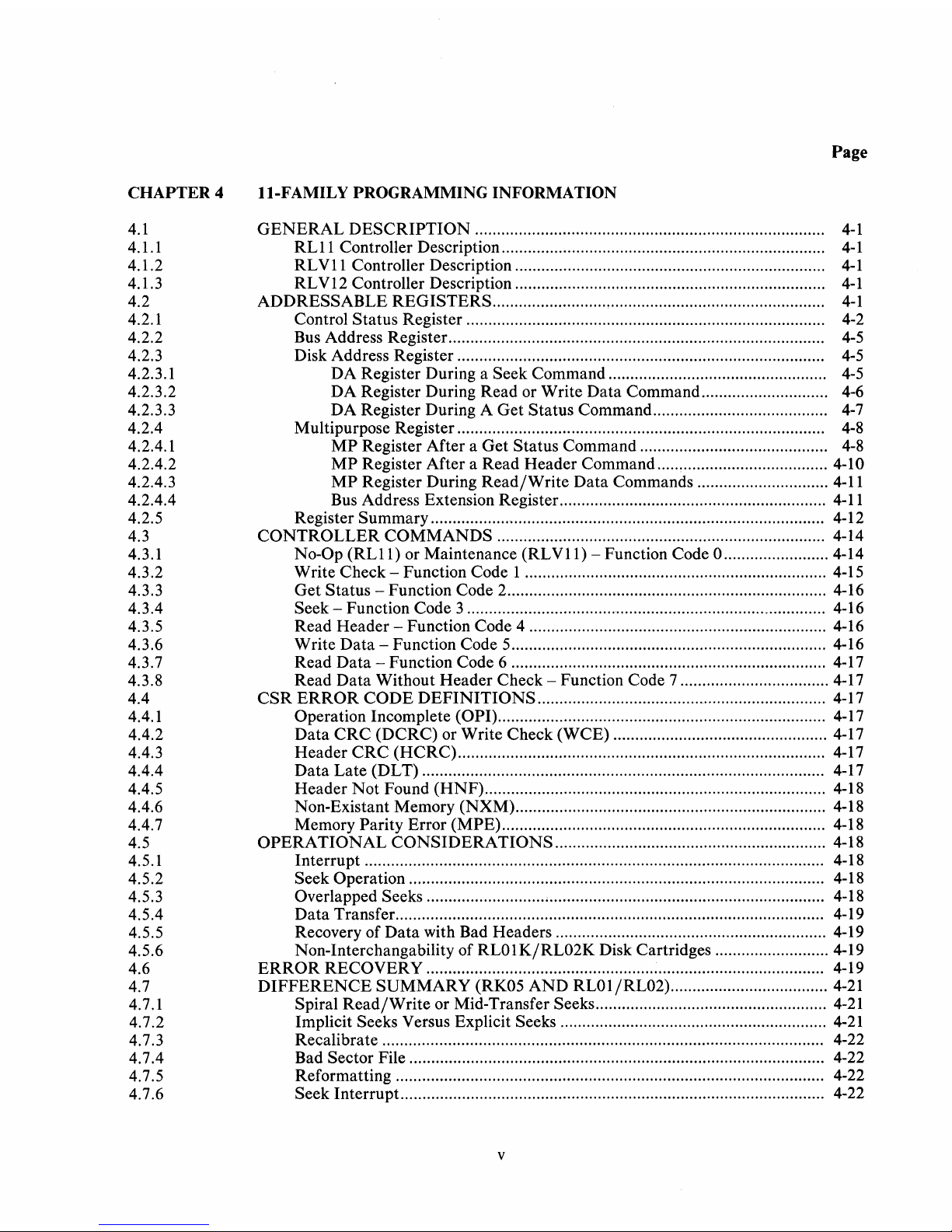
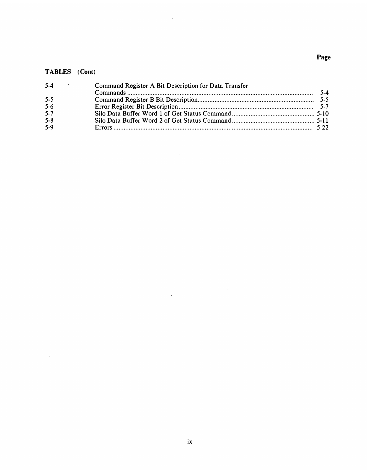
1.3 SUBSYSTEM DESCRIPTION
The
RLOI/RL02
mass storage subsystem
is
based on the
RLOIK/RL02K
disk cartridges, the
RLOI/RL02
drive unit(s), and an appropriate controller such as the
RLII
(PDP-II),
RLVII
or
RLV12
(LSI-II),
or
RL8A
(PDP-S). The basic subsystem
is
illustrated in Figure
1-1.
1-1
Page 12
•
UNIBUS
•
OMNIBUS
•
Q-BUS
CONTROLLER
RL11
CU/DRIVE
INTERFACE
RLV11
RLV12
RL8A
•
•
READ
DATA
•
STATUS
• SECTOR PULSES
• GET
STATUS
• SEEK
•
WRITE
DATA
Figure
1-1
Typical RLO]
/RL02
Mass
Storage
Subsystem
Configura tion
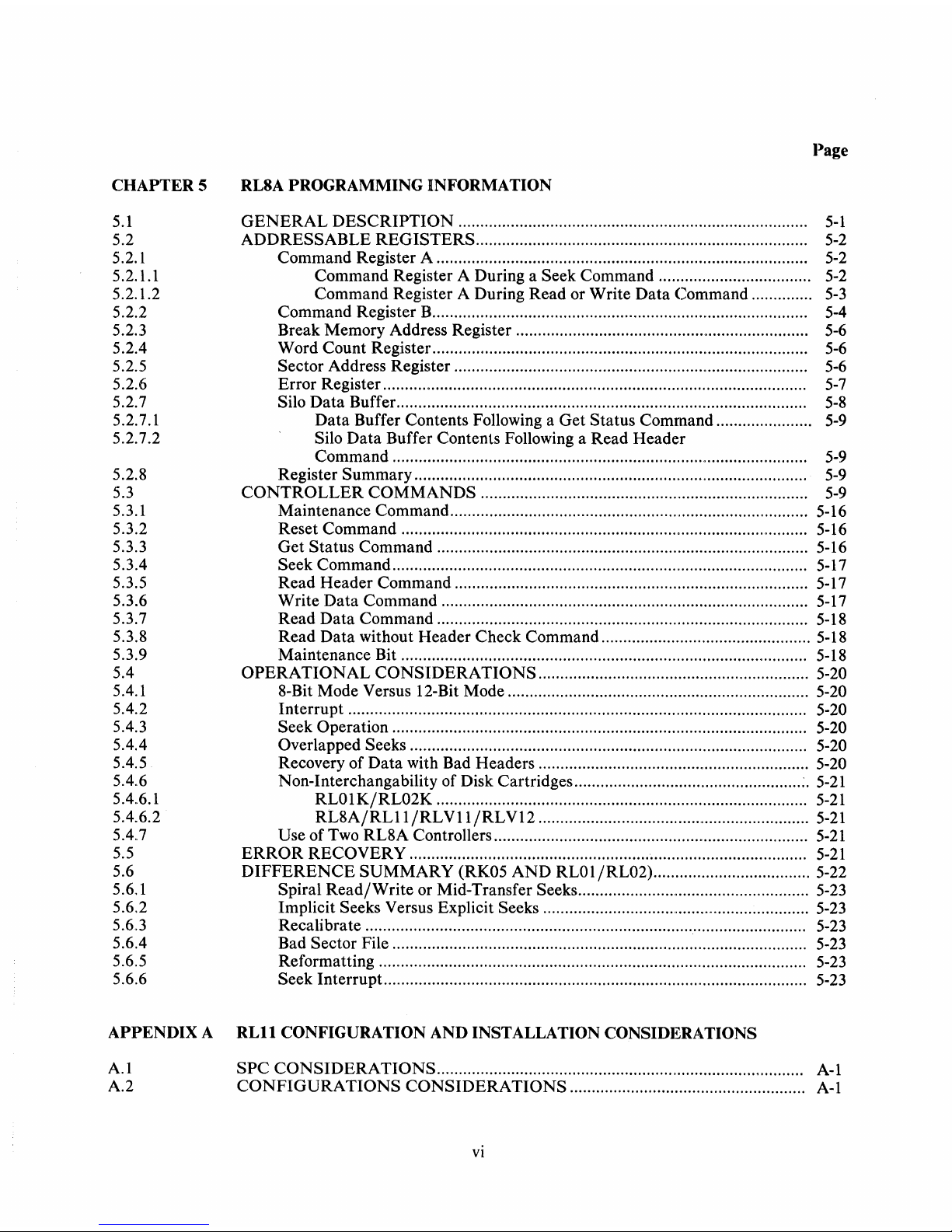
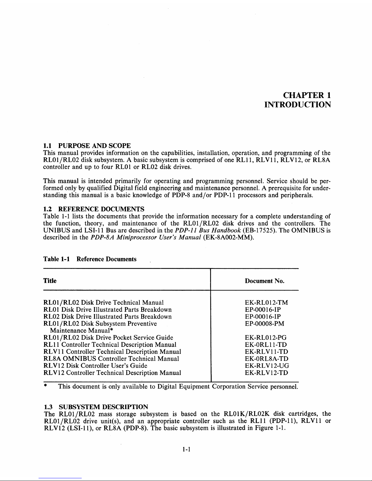
1.3.1 RLOljRL02 Disk Drive
(DRIVE
0)
o
(DRIVE 1)
01
(DRIVE
2)
01
(DRIVE
3)
0]
CZ-1007
The
RLOI
/RL02
drive unit
is
built into a chassis
that
slides
out
of
the
cabinet
to allow
operator
access
to
the
top cover for loading and unloading
of
the
disk cartridge.
If
the
stops on
the
slide
are
manually
released,
the
chassis
can
be
pulled
farther
out
so
that
the
rear
top cover
can
be
removed for servicing.
The
front panel contains.
operator
controls
and
indicators.
The
chassis contains a spindle, two
read/write
heads mounted on a positioner, logic modules, a power
supply with
an
ac
power cord and
circuit
breaker, a closed-loop clean
air
system, a cooling
air
syste:m,
appropriate
safety interlocks,
and
connectors for
the
I/O
cable(s).
The
drive
unit
is shown in Figure 1-2.
The
RL02
drive unit has a label reading
"RL02"
on
the
front panel.
The
RLOI drive
currently
does not
have a label identifying it as
an
RLO
1.
1.3.2 RL Controllers
There
are
four controllers available for
the
RLO 1
/RL02
subsystem. All
can
handle
up
to four drives
and
all feature
Direct
Memory
Access
(DMA)
operation.
1.3.2.1
RLl1
Controller Description -
The
RLII
controller consists
of
a single, hex-height
Small
Peri-
pheral Controller
(SPC)
module designated M7762.
It
is
used to interface
the
drive with
the
PDP-II
UNIBUS.
The
data
is
formatted
in 16-bit words.
1-2
Page 13
Figure
1-2
RLOI/RL02
Disk Drive
1.3.2.2 RLVII Controller Description - The
RLVII
controller consists of two quad-height modules
designated
M8013 and M8014. This controller interfaces the drive with the
LSI-II
Bus. The data
is
formatted in 16-bit words. The controller can handle any combination of up to four RLOI
/RL02
drives.
1.3.2.3 RL8A Controller Description - The RL8A controller consists of a single, hex-height module
designated M8433.
It
is
used to interface the drive with the PDP-8 OMNIBUS. The data can be formatted in either 8-bit bytes or 12-bit words. This controller has a jumper-determined choice of handling
RLOI or RL02 drives. However, in the RL02-jumpered configuration,
it
can handle any combination of
up to four
RLO 1 /RL02
drives.
1.3.2.4 RLV12 Controller Description - The RLV12 controller consists of a single, quad-height mod-
ule designated
M8061.
It
is
used to interface the drive with either the extended
LSI-II
Bus or the
standard
LSI-II
Bus. A jumper designates the 22-bit or 18-bit addressing scheme. The data
is
for-
matted in 16-bit words. This controller can handle any combination of up to four
RLO 1 /RL02
drives.
1-3
Page 14
1.3.3 RLOIK/RL02K Disk Cartridge
The
RLO
1 K or RL02K
is
a removable, top-loading 5440-type disk cartridge
that
is
formatted in a man-
ner unique to the
RL01/RL02
subsystem. Both cartridges contain a single platter. The RL01K cartridge has a capacity of 5.2 megabytes of user data, and the RL02K cartridge holds 10.4 megabytes of
data. Both sides of the platter are used for data. There are 256 tracks on each
RL01K platter surface
and 512 tracks on each
RL02K platter surface. Each track
is
divided into 40 sectors. Each sector
con-
tains 256 bytes of data. The last track of the last surface
is
reserved for the cartridge serial number and
bad sector information. Head positioning servo information and header information are prerecorded at
the factory and cannot be reformatted in the field. This information, along with the data,
is
read by
the:
read/write heads but the internal logic of the drive unit protects the servo and header information
from.
being overwritten.
1.3.3.1 Interchangability - The RL01K and RL02K disk cartridges are not functionally inter··
changable although they are physically interchangable.
It
is
possible to mount an RL01K cartridge
Ont
an RL02 drive, for example,
but
proper operation will not occur. An RL01K cartridge written on
an.
RL01 unit can be read on any other RLOI unit even if
that
unit
is
controlled by a different type of
controller. The limitation to this interchangeability
is
that
if an RL8A controller
is
used to write data.
and the cartridge
is
to be used by an II-Family controller, the RL8A must use the 8-bit byte mode of
operation.
An
RL02K cartridge written on an RL02 unit can be read
on
any other RL02 unit (assuming the
conditions mentioned above).
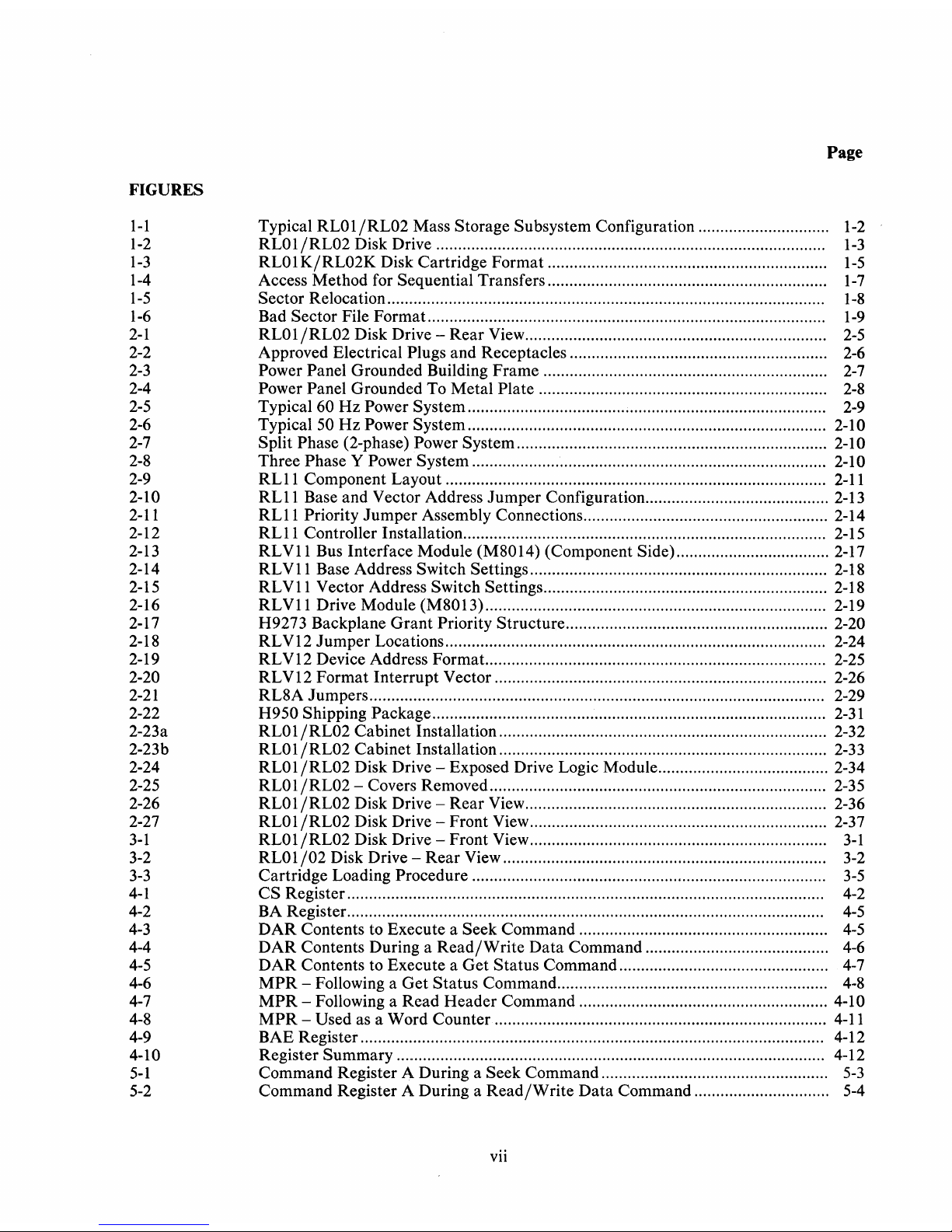
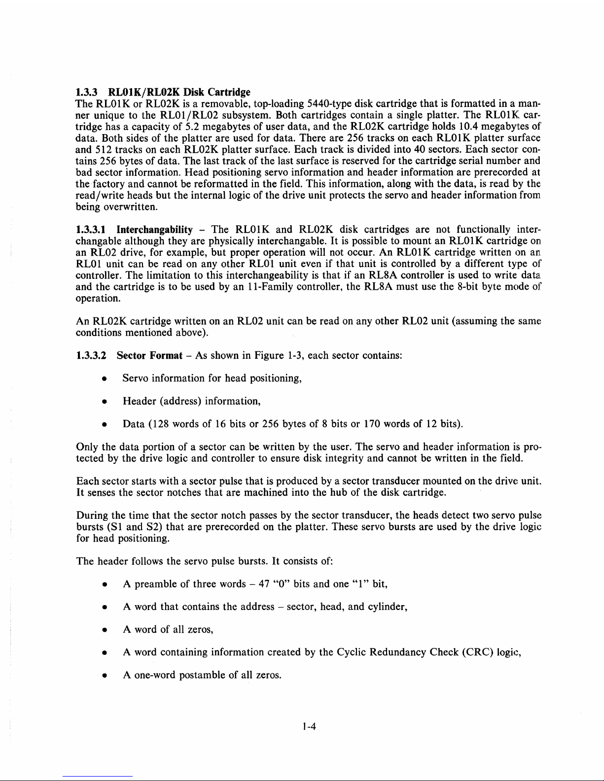
1.3.3.2 Sector Format - As shown in Figure 1-3, each sector contains:
• Servo information for head positioning,
• Header (address) information,
• Data (128 words of
16
bits or 256 bytes of 8 bits or 170 words of
12
bits).
Only the data portion of a sector can be written by the user. The servo and header information
is
pro.-
tected by the drive logic and controller to ensure disk integrity and cannot be written in the field.
Each sector starts with a sector pulse
that
is
produced by a sector transducer mounted on the unit.
It
senses the sector notches
that
are machined into the hub of the disk cartridge.
During the time
that
the sector notch passes by the sector transducer, the heads detect two servo pulse
bursts
(Sl
and S2)
that
are prerecorded
on
the platter. These servo bursts are used by the drive logic
for head positioning.
The header follows the servo pulse bursts.
It
consists
of:
• A preamble of three words -
47
"0"
bits and one
"1"
bit,
• A word that contains the address - sector, head, and cylinder,
• A word of all zeros,
• A word containing information created by the Cyclic Redundancy Check (CRC) logic,
• A one-word postamble of all zeros.
]-4
Page 15
-
I
V.
I
....
----------------
6251£5
---------------.-.11
I I
.-62.51£5
....
I
I 1 I
J
SECTOR I I
PULSE
I •
:.
I I
>0--
-----------------,
__
'
__________________
l
.;"/
--------
---
......
-
......
-
....
"
PREAMBLE
ADDRESS
47 ZERO BITS
11
16
BITS
./
./
SECTOR
HEAD
SIX BITS
ONE
BIT
L
lSB
ZEROES
16 ZERO BITS
.....
.......
CYLINDER
NINE BITS
CRC
16 BITS
--
POSTAMBlE
16 ZERO BITS
16
BITIWORD
MODE
S BIT/BYTE
MODE
12 BITIWORD
MODE
Figure
1-3
RLOIK/RL02K Disk Cartridge Format
-
PREAMBLE
47
ZERO BITS
--
---
-
WORD 0
WORD 1
16
BITS
16
BITS
BYTE BYTE
I
0
1
I
SBITS
SBITS
·.If
I
WORD
0 WORD 1
I
12 BITS
12 BITS
t
L
MSB
I
lSB
..
DATA
CRC
POSTAMBlE
11
..
16
BITS
16
ZERO BITS
2048 BITS
.IL
.
-
......
"'-
......
I
I
WORD 126
WORD 127
.1
S.
16 BITS
16
BITS
f
•
I
BYTE
BYTE
J
254 255
8
BITS
8
BITS
,
,
WORD
168
WORD
169
UN-
USED
I
12
BITS
12
BITS
8 BITS
f
CZ·2C127
Page 16
The user writeable data area
follows
the header.
It
consists
of:
• A preamble of three words -
47
"0"
bits and one
"1"
bit,
• Data (128 words of
16
bits or 256 bytes of 8 bits or
170
words of
12
bits),
• A word containing CRC-generated information,
• A one-word postamble of all zero bits.
Following each sector
is
a period of idle tirne that
is
simply a wait for the next sector pulse.
In addition to the data tracks, there are tracks both inside and outside of the data area that contain
unique servo signals that define those areas as guard bands.
If
the read/write heads attempt to enter
a.
guard band, the drive logic causes the positioner to retreat from the guard band and return to data
are:a.
The disk has a nominal rotational speed of 2400 rev/min. Therefore, the time for one revolution
is
25
milliseconds. Since the revolution
is
divided into
40
sectors, the duration of each sector
is
625
nlicro·,
seconds. This 625 microsecond period
is
divided into non-data (sector pulse,
headel!",
idle time) time
and.
data time. The data time period
is
500 microseconds. Thus, the data
is
transferred in 500
bursts that occur every 625 microseconds.
For 16-bit word mode there are
128
words of data in a sector
so
the peak transfer rate
is
3.9
n(licro··
seconds per word and the average transfer rate
is
4.9 microseconds per word.
For 8-bit bytes (256 bytes per sector), the peak transfer rate
is
1.9
microseconds per byte and the aver
..
age transfer rate
is
2.4 microseconds per byte.
For 12-bit word mode
(170 words per sector), the peak transfer rate
is
2.9 microseconds per word and
the average transfer rate
is
3.7
microseconds per word.
1-6
Page 17
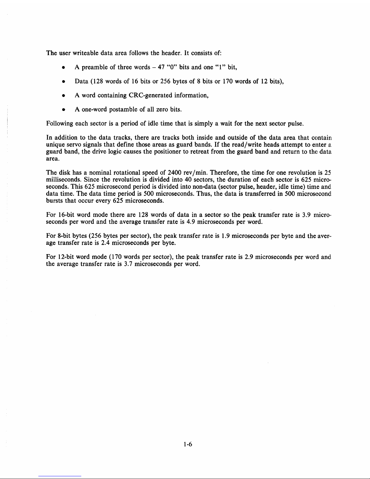
1.4 SECTOR LOCATION
The
RLOIK/RL02K
disk cartridges do not have a physical index notch (occurring once per revolution)
machined into the hub as some cartridges do.
The
controller determines the rotational position
of
the
disk cartridge by reading, from the header,
the
sector address as well as the head (surface) and cylinder
(track) addresses. Thus, the cartridge does not need a physical index.
The
sectors
are
relocated to opti-
mize the
data
transfer
rate
when it becomes necessary to perform a seek during a
data
transfer.
A head switch to the other surface is considered a seek because the
RLOI/RL02
subsystem uses servo
information
that
is
recorded on each track.
The
newly selected head will position itself over the center
of
the
track. There
is
no hardware-controlled implicit seek on the
RLOI/RL02
subsystem. All seeks,
including spiral (mid-transfer) seeks, must be programmed into the software.
The
correct head must be
selected and positioned over the correct
track
by a seek operation before the software
can
initiate a
data
transfer.
When
the end
of a track
is
reached and the
data
transfer has not been completed, the software must do
one
of
two things.
It
must switch to the head
that
is
over the corresponding
track
on
the
other surface
(6.5 milliseconds average, 8 milliseconds maximum) or the software must issue a seek to the next cylinder (15 milliseconds).
If
the head is to be switched also, the seek
and
the head switching are normally
combined.
Once the unit has completed
the
seek operation, the software
can
continue the
data
transfer.
To reduce
the
rotational latency following a head switch seek, surface one is offset by
17
sectors from
surface zero.
The
eight milliseconds head switch corresponds to
13
sectors
of
this offset and the addi-
tional four sectors allow for software overhead.
To reduce the rotational latency following a one cylinder seek (with head switch), surface 0
of
a cylin-
der is offset by 29 sectors from surface 1
of
the previous cylinder.
The
15
millisecond seek time takes
24 sectors
of
this offset
and
five more sector times are allowed for software overhead.
These two offset patterns are illustrated in Figures
1-4
and
1-5.
SURFACE
"0"
(HDS = 0)
SURFACE
"1"
(HDS
-1)
CYL
=0
I
1
2
I
Figure
1-4
Access Method for Sequential
Transfers
1-7
3
I
..
TO
SPINDLE
MA-0567
Page 18
Sp·
3
(PHYSICAL
SECTOR)
NOTE:
NUMBERS
IN
BLOCKS
REFER
TO
HEAD
1.
Figure
1-5
Sector Relocation
1.5
BAD
SECTOR FILE
INDEX
MA-0579
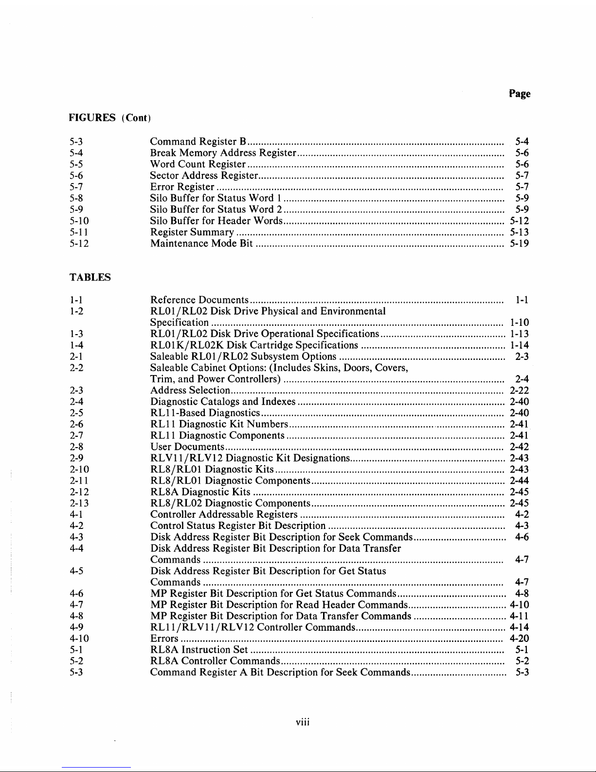
The Bad Sector File
is
a list of all bad sectors found
on
an
RLO 1 K/RL02K
disk cartridge.
It
also contains the cartridge serial number. The operating system uses this information to avoid allocating bad
sectors to a user's files.
If
there
is
an error in a header, or if there are
16
consecutive read/write errors within one sector, that
sector
is
defined as a bad sector.
This file
is
recorded
on
surface
1,
track
255
(decimal) of an RLOIK cartridge, and surface
1,
tra(!k
511
(decimal) of an RL02K cartridge. The file consists of
40
sectors of
128
words each. Figure
1-6
shows
the format of the Bad
Sector File.
There
is
room
in
the file for
128
entries written by the factory and for
128
entries that can be written
in
the field if bad sectors develop during field use.
1-8
Page 19
I
-.0
LAST
CYLINDER
LAST
SURFACE
SEC
TOR
0
1
2
3
4
5
6
7
8
9
10
11
12
13
14
15
16
17
18
19
20
21
22
23
24
25
26
27
28
29
30
31
32
33
34
35
36
37
38
39
BAD SECTOR FILE
CONTENTS
FACTORY
WRITTEN BAD SECTOR INFO
ALL ONES
DUPLICATE OF SECTORS 0, 1
ALL ONES
DUPLICATE OF SECTORS
0,1
ALL ONES
DUPLICATE OF SECTORS
0,1
ALL ONES
DUPLICATE OF SECTORS
0,1
ALL ONES
FIELD WRITTEN BAD SECTOR INFO
ALL ONES
DUPLICATE OF SECTORS 20,
21
ALL ONES
DUPLICATE OF SECTORS 20,
21
ALL ONES
DUPLICATE OF SECTORS 20,
21
ALL ONES
DUPLICATE OF SECTORS 20,
21
ALL ONES
Figure
1-6
Bad Sector File Format
TWO
SECTORS
25616
BIT
WORDS
125
ENTRIES
SECTOR
ENTRY
SECOND
BAD
SECTOR
ENTRY
.
125th BAD {
SECTOR
ENTRY
MSB
16
BIT
WORD
LSB
OR
15
14
113
112
1
11
1
10
1
9
8 1
7
1 6 1
5
1 4 1
3
1
2
11
1
0
0
ZERO
5
MOST
SIGNIFICANT OCTAL DIGITS OF CARTRIDGE SERIAL
NUMBER
1 ZERO
5 LEAST SIGNIFICANT
OCTAL
DIGITS OF CARTRIDGE SERIAL
NUMBER
2
ZEROES
3
ZEROES
4
ZEROES
CYLINDER ADDRESS
5 ZEROES
HEADl
ZEROES
I
SECTOR ADDRESS
6
f--
SAME
FORMAT
AS
"'IRST
BAD
SECTOR ENTRY
7
,
r'
,
.
252
f--
SAME
FORMAT
AS
FIRST BAD SECTOR ENTRY
253
254
ALL
ONES
255
ALL
ONES
NOTE:
UNUSED
BAD SECTOR ENTRIES ARE
ALL
ONES
CZ-2028
Page 20

1.6 RLOI
jRL02
SPECIFICATIONS
The following tables list the specifications of the
RL01jRL02
drives and the
RL01KjRL02K
car-
tridges.
1.
Table
1-2
RL01jRL02
Disk Drive Physical and Environmental Specifications
2.
Table
1-3
RLO 1 KjRL02K
Disk Drive Operational Specifications
3.
Table
1-4
RL01K/RL02K
Disk Cartridge Specifications
Table 1-2 RLOljRL02 Disk Drive
Physical and Environmental
Specifications
Characteristics
Width
Depth
Height
Weight
Mounting
Power
Source
Input Power
Power Factor
Starting Current
Heat
Dissipation
Power Cord and
Connector
Specifications
Compatible with
19
inch
RETMA
rack
63.5 cm (25 in) behind bezel
26.52 cm (10.44 in)
34
kg
(75 lb)
The drive mounts
on
chassis slides
90-127 Vac (47.5-63 Hz)
180-256 Vac (47.5-63 Hz)
(Manually selectable)
160W
max
at
115 Vac, 60 Hz
Greater than 0.85
3.5A (rms) max
@ 90 Vacj47.5-63
Hz
5.0A (rms) max @
127
Vac/47.5-63 Hz
1.75A (rms) max
@ 180 Vac/47.5-63 Hz
2.5A (rms) max
@ 254 Vac/47.5-63 Hz
546
Btu/hr
max
A molded line cord compatible with the drive operating voltage and the
861
power control for 120
Vac
is
attached to the drive. The power cord
is
2.74 m
(9
ft)
long and the plug
is
NEMA
5-15P.
The
230 Vac plug to be attached to high voltage
drives
is
NEMA
6-15P.
1-10
Page 21
Table 1-2 RLOl/RL02 Disk Drive
Physical and Environmental
Specifications (Cont)
Characteristics
Safety
Interlocks
Temperature
/
Humidity
Altitude
Shock
Vibration
Specifications
The
RL01
/RL02
disk drive
is
UL
listed and
CSA
certified.
Interlocks are used where potential exists for
damage to drive, media, operators, or service
personnel.
Operating:
Temperature: 100 C (500 F) to 400 C (1040 F)
Note: Maximum allowable operating temperatures are
reduced by a factor
of
1.80 C/1000
meters (10 F
/1000
feet) for operation above sea level.
Relative Humidity:
10 to 90 percent with maximum wet
bulb
temperature
280 C (820 F) and minimum dew point
20 C (360 F)
Nonoperating:
Temperature:
-400 C
(-400 F) to 660 C (1510 F)
Relative Humidity: 10 to 95 percent, non condensing
Operating:
2440 m (8,000 ft) max
Nonoperating: 9144 m
(30,000
ft)
max
Operating:
Half
sine shock pulse
of
gravity peak and 10 ± 3 ms
duration applied once in either direction of three
orthogonal axes (3 pulses total)
Nonoperating:
Half
sine shock pulses of 40 gravity peak and 30 ±
10 ms duration perpendicular to each of six package
surfaces.
Operating:
Sinusoidal vibration (sweep
rate
1 octave/min)
5-50 Hz, 0.002 in displacement amplitude
50-500 Hz, 0.25 gravity peak
500-50 Hz, 0.25 gravity peak
50-5 Hz, 0.002 in displacement amplitude
I-I
I
Page 22
Table 1-2 RLOI/RL02 Disk Drive
Physical
and
Environmental
Specifications (Cont)
Characteristics
Vibration
EMI
Dust
Attitude
Specifications
Nonoperating:
Vertical Axis Excitation - 1.40 gravity (rms) overall from
10 to 300 Hz; power spectral density
of
0.029
g2/Hz
from 10 to 50 Hz, with 8
dB/octave
roll-
off from
50 to 300
Hz
Longitudinal and
Lateral
Axis Excitation - 0.68
gravity (rms) overall from
10 to 200 Hz; power
spectral density
of
0.007
g2/Hz
from 10 to 50 Hz,
with 8
dB/octave
rolloff from 50 to 200
Hz
Meets
DEC
Standard
102, Section
7.
The
drive will operate in
an
ambient atmosphere
of
less
than
5 million particles 0.5 microns or larger
per cubic foot
of
air.
The
drive is intended to run
in a light industry or cleaner environment.
Maximum
pitch: ±
15
degrees
Maximum
roll: ±
15
degrees
1-12
Page 23
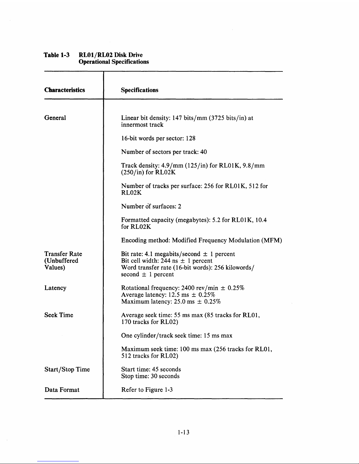
Table 1-3 RLOI/RL02 Disk Drive
Operational Specifications
Characteristics
General
Transfer
Rate
(Unbuffered
Values)
Latency
Seek Time
Start/Stop
Time
Data
Format
Specifications
Linear bit density: 147
bits/mm
(3725 bits/in)
at
innermost track
16-bit words per sector: 128
Number
of sectors per track: 40
Track density:
4.9/mm
(125/in) for RL01K,
9.8/mm
(250/in) for
RL02K
Number
of tracks per surface: 256 for RL01K, 512 for
RL02K
Number
of surfaces: 2
Formatted capacity (megabytes): 5.2 for
RL01K,
lOA
for RL02K
Encoding method: Modified Frequency Modulation (MFM)
Bit rate:
4.1
megabits/second ± 1 percent
Bit cell width: 244 ns
± 1 percent
Word transfer rate (16-bit words): 256 kilowords/
second ± 1 percent
Rotational frequency:
2400 rev/min ± 0.25%
Average latency: 12.5 ms ± 0.25%
Maximum latency: 25.0 ms ± 0.25%
Average seek time:
55
ms max (85 tracks for RL01,
170 tracks for RL02)
One cylinder/track seek time:
15
ms max
Maximum seek time:
100 ms max (256 tracks for RL01,
512 tracks for RL02)
Start
time:
45
seconds
Stop time: 30 seconds
Refer to Figure
1-3
1-13
Page 24
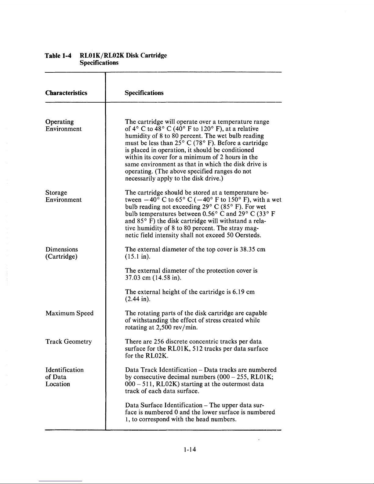
Table 1-4 RLOIKjRL02K Disk Cartridge
Specifications
Characteristics
Operating
Environment
Storage
Environment
Dirnensions
(Cartridge)
Maximum
Speed
Track Geometry
Identification
of Data
Location
Specifications
The cartridge
will
operate over a temperature range
of
4° C to 48° C (40° F to 120° F),
at
a relative
humidity of 8 to
80
percent. The wet bulb reading
must be less than
25° C (78° F). Before a cartridge
is
placed in operation, it should be conditioned
within its cover for a minimum of 2 hours in the
same environment as that in which the disk drive
is
operating. (The above specified ranges do not
necessarily apply to the disk drive.)
The cartridge should be stored
at
a temperature be-
tween
-400 C to
650 C
(-400 F to 150° F), with a wet
bulb reading not exceeding
29° C (85° F). For wet
bulb. temperatures between
0.56° C and
29
0
C (33
0
F
and
85° F) the disk cartridge will withstand a rela-
tive humidity of 8 to
80
percent. The stray mag-
netic field intensity shall not exceed
50 Oersteds.
The external diameter of the top cover
is
38.35 cm
(15.1 in).
The external diameter of the protection cover
is
37.03 cm (14.58 in).
The external height of the cartridge
is
6.19 cm
(2.44 in).
The rotating parts of the disk cartridge are capable
of withstanding the effect of stress created while
rotating
at
2,500 rev Imin.
There are 256 discrete concentric tracks per data
surface for the
RLO 1 K,
512 tracks per data surface
for the
RL02K.
Data Track Identification - Data tracks are numbered
by consecutive decimal numbers
(000 - 255, RLOIK;
000
- 511, RL02K) starting
at
the outermost data
track of each data surface.
Data Surface Identification - The upper data surface
is
numbered 0 and the lower surface
is
numbered
1, to correspond with the head numbers.
1-14
Page 25
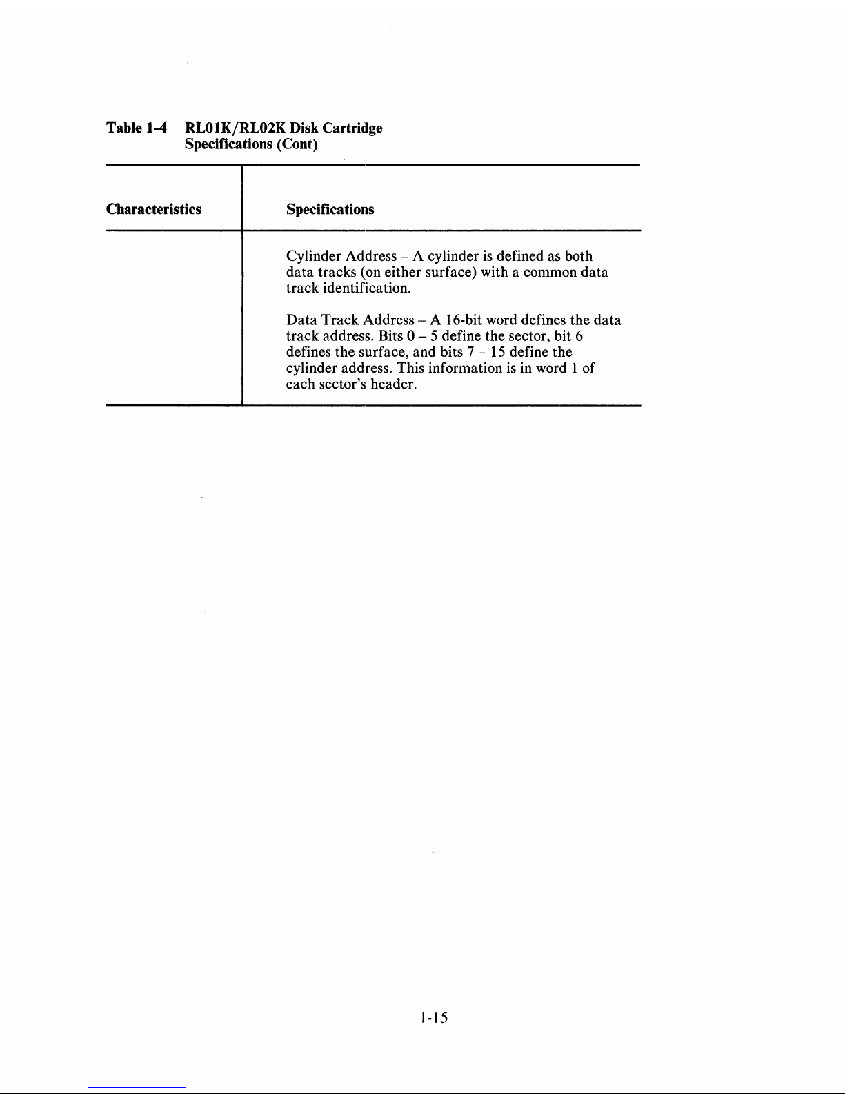
Table 1-4 RLOIKjRL02K Disk Cartridge
Specifications (Cont)
Characteristics Specifications
Cylinder Address - A cylinder
is
defined as both
data tracks (on either surface) with a common data
track identification.
Data Track Address - A 16-bit word defines the data
track address. Bits
0 - 5 define the sector, bit 6
defines the surface, and bits 7 -
15
define the
cylinder address. This information
is
in word 1 of
each sector's header.
1-15
Page 26

Page 27
2.1
SITE
PREPARATION
AND
PLANNING
CHAPTER 2
INSTALLATION
This
chapter
describes power, space, environmental, cabling, and safety requirements
that
must be con-
sidered before installation
of
the
RLOl/RL02
disk subsystem.
2.1.1 Environmental Considerations
The
RLOl/RL02
disk subsystem is designed to operate in a business or light industry environment.
Although cleanliness is
an
important consideration in the installation
of
any computer system, it is par-
ticularly crucial for proper operation
of
a disk drive.
The
RLO 1 K/RL02K
disk cartridge is not sealed
while being loaded and is therefore vulnerable to dust or smoke particles suspended in the air, as well as
to fingerprints, hair, lint, etc. These minute obstructions can cause head crashes, resulting in severe
damage to the
read/write
heads and disk surfaces.
2.1.1.1
Cleanliness -
The
RLOl/RL02
disk drives
can
operate in
an
ambient with less than five mil-
lion particles per cubic foot of air which are
0.5 micron or larger in diameter.
The
drive contains a filter
system which, under these conditions, maintains the particle count within the cartridge below 100 particles per cubic foot.
2.1.1.2 Space Requirements - Provision should be made for service clearances
of
1 m (39 in)
at
the
front
and
rear
of
the rack or cabinet in which the drive
is
mounted and 1 m (39 in)
at
either side.
Storage space for the
RLOIK/RL02K
cartridges should also be made available.
Each
cartridge has a
diameter
of
approximately 38
cm
(15 in) and a height
of
approximately 6
cm
(2.5 in).
CAUTION
RL01K/RL02K
disk cartridges must never be
stacked on top
of
each other. A designated shelf area
or
specially designed disk cartridge storage unit is
recommended (see the DIGITAL
Supplies and Ac-
cessories Catalog).
2.1.1.3
Floor Loading -
The
weight
of
the
RLOl/RL02
disk drive alone
is
34 kg (75 lb), which will
not place undue stress on most floors. However, the added weight
of
the rack or cabinet as well as the·
number
of
drives to be installed should be considered in relation to the weight
of
existing computer
systems. Possible future expansion should also be a consideration.
2.1.1.4
Heat
Dissipation -
The
heat
dissipation
of
each
RLOl/RL02
disk drive is 546
Btu/hour
max-
imum.
The
approximate cooling requirements for the entire system can be calculated by multiplying
this figure by the number
of
drives, adding the result to the total
heat
dissipation
of
the other system
components,
and
then adjusting
the
total figure to compensate for personnel, cooling system efficiency,
etc.
It
is advisable to allow a safety margin of
at
least
25
percent above the maximum estimated re-
quirements.
2-1
Page 28
2.1.1.5 Acoustics - Most computer sites require
at
least some degree of acoustical treatment. How-
ever, the
RLOl/RL02
disk subsystem should not contribute unduly to the overall system
leve:1.
Ensure
that
acoustical materials used do not produce or harbor dust.
2 . .1.1.6 Temperature - The
RLOl/RL02
disk subsystem operates over a temperature range of
10
0
C
(500 F) to 400 C (1040 F). The maximum temperature gradient
is
16.60 C (300 F) per hour. The non-
operating temperature range
is
from
-400 C
(-40
0
F) to 66
0
C (151
0
F).
2 . .1.1.7 Relative Humidity - Humidity control
is
important for proper operation of any computer system since static electricity may cause memory errors or even permanent danlage to logic components.
The
RLOI/RL02
disk subsystem
is
designed to operate within a relative humidity range of
10
to 90
percent with a maximum wet bulb temperature of
280 C (82
0
F) and a minimum dew point of 2
0
C
(36
0
F). The nonoperating relative humidity range
is
from
10
to 95 percent, with a maximum wet
bullb
temperature of 460 C (115
0
F).
2.1.1.8 Altitude - Computer systems operating
at
high altitudes may have heat dissipation problems.
Altitude also affects the flying height of
read/write
heads in disk drives. The maximum altitude speci-
fied for operating the
RLOI/RL02
disk subsystem
is
2440 m (8000 ft). Also, the maximum allowable
operating temperature
is
reduced by a factor of 1.80 C per 1000m
(l0
F per 1000 ft) above sea
level
Thus, the maximum allowable operating temperature
at
2440 m (8000 ft) would be reduced to 360 C
(96
0
F).
2.1.1.9 Power and Safety Precautions - The
RLOI/RL02
disk subsystem presents
no
unusual fire or
safety hazards to an existing cOlnputer system.
AC
power wiring should be checked carefully, however,
to ensure
that
its capacity
is
adequate for the added load as well as for any possible expansion. The
RLO 1 /RL02
disk drive
is
UL
listed and
CSA
certified.
2.1.1.10 Radiated Emissions - Any source of electromagnetic interference
(EMI)
that
is
near the
computer system may affect the operation of the processor and its related peripheral equipment
..
Conl-
m.on
EMI
sources
that
are known causes of failures include:
•
Thunderstorms,
•
Broadcast stations,
•
Radar,
•
Mobile communications,
•
High-voltage power lines,
•
Power tools,
•
Arc welders,
•
Vehicle ignition systems,
•
Static
electricity.
The effect of radiated
EMI
emissions on a computer system
is
unpredictable. Thus, grounding plays an
inlportant role in protecting the circuits used in disk drive subsystems.
To help reduce the effects of known high-intensity
EMI
emissions, perform the following actions:
• Ground window screens and other large metal surfaces,
• Ensure
that
the overall computer system
is
grounded properly (refer to Paragraph 2.1.5,
Grounding Requirements),
• Provide proper storage (metal cabinets with doors) for disk cartridges.
2-2
Page 29
2.1.1.11 Attitude/Mechanical Shock - Performance of the
RL01/RL02
disk subsystem will not be
affected by an attitude where maximum pitch and roll do not exceed
15
degrees.
The subsystem
is
designed to operate while a half-sine shock pulse of
10
gravity peak and
10
± 3 ms
duration
is
applied once in either direction of three orthogonal axes (three pulses total).
2.1.2 Options
The
RL01/RL02
disk drive can be shipped with various controllers (for UNIBUS,
OMMIBUS
and
LSI-II
Bus computer systems), and can be configured for
115
Vac or 230 Vac operation.
Table
2-1
shows saleable
RL01/RL02
subsystem options. Table
2-2
shows
RL01/RL02
cabinet com-
ponents.
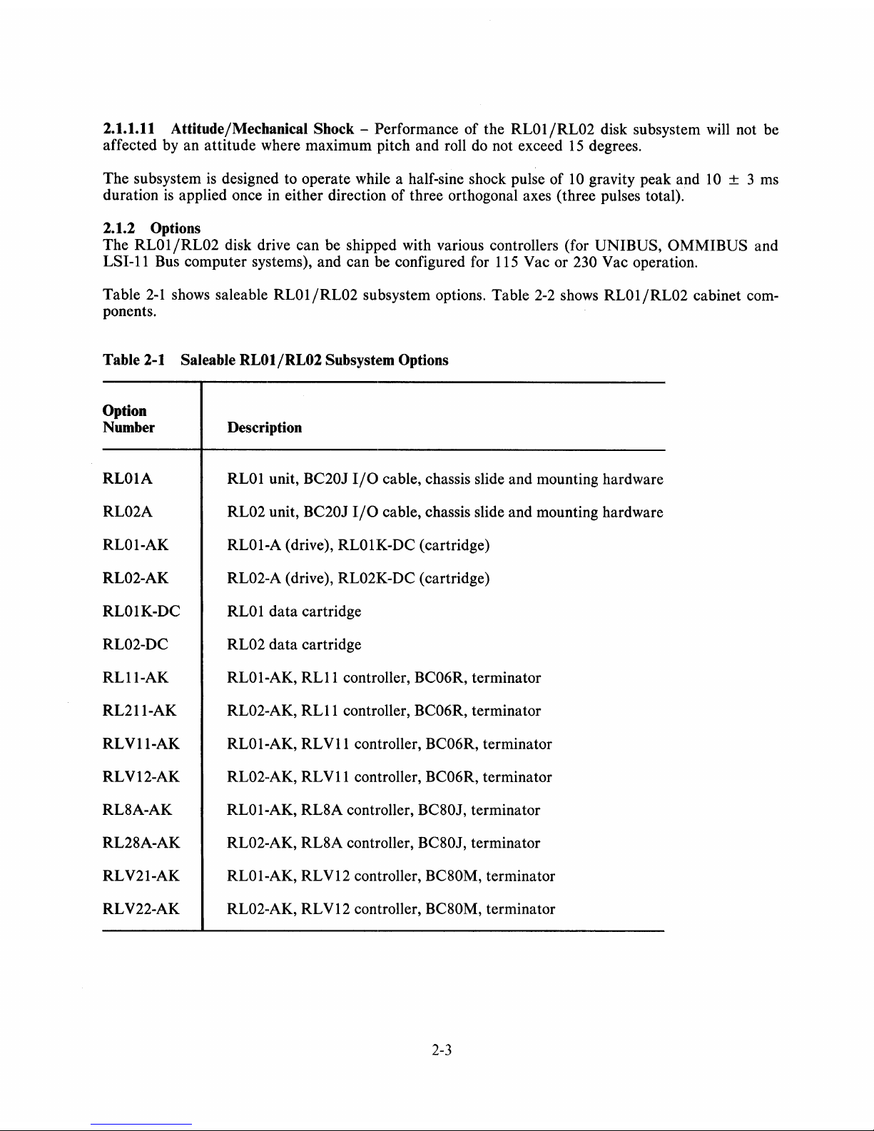
Table 2-1 Saleable
RLOI/RL02 Subsystem Options
Option
Number
RL01A
RL02A
RL01-AK
RL02-AK
RL01K-DC
RL02-DC
RL11-AK
RL211-AK
RLV11-AK
RLV12-AK
RL8A-AK
RL28A-AK
RLV21-AK
RLV22-AK
Description
RL01 unit, BC20J
I/O
cable, chassis slide and mounting hardware
RL02 unit, BC20J
I/O
cable, chassis slide and mounting hardware
RL01-A (drive), RL01K-DC (cartridge)
RL02-A (drive), RL02K-DC (cartridge)
RL01 data cartridge
RL02 data cartridge
RL01-AK, RL11 controller, BC06R, terminator
RL02-AK, RL11 controller, BC06R, terminator
RL01-AK, RLV11 controller,
BC06R, terminator
RL02-AK, RLV11 controller, BC06R, terminator
RL01-AK, RL8A controller, BC80J, terminator
RL02-AK, RL8A controller, BC80J, terminator
RL01-AK, RLV12 controller, BC80M, terminator
RL02-AK, RLV12 controller, BC80M, terminator
2-3
Page 30
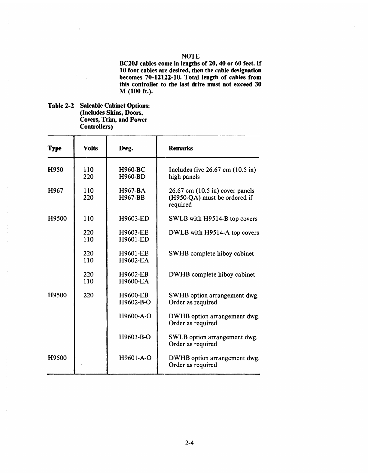
NOTE
BC20J cables come in lengths
of
20, 40 or 60 feet.
If
10 foot cables are desired, then the cable designation
becomes 70-12122-10. Total length
of
cables from
this controller to the last drive must not exceed
30
M (100 ft.).
Table 2-2 Saleable Cabinet Options:
(Includes Skins, Doors,
Covers, Trim, and Power
Controllers)
Ty
pe Volts
Dwg.
Remarks
H
950 110
H960-BC
Includes five 26.67 cm {l0.5 in)
220
H960-BD
high panels
H 967
110
H967-BA
26.67 cm
(10.5 in) cover panels
220 H967-BB
(H950-QA) must be ordered if
required
H
9500 110 H9603-ED SWLB with H9514-B top covers
220 H9603-EE
DWLB with H9514-A top covers
110 H9601-ED
220 H9601-EE
SWHB complete hiboy cabinet
110 H9602-EA
220
H9602-EB
DWHB complete hiboy cabinet
110 H9600-EA
H
9500 220 H9600-EB SWHB option arrangement dwg.
H9602-B-O Order as required
H9600-A-O DWHB option arrangement dwg.
Order as required
H9603-B-O SWLB option arrangement dwg.
Order as required
H
9500 H9601-A-O
DWHB option arrangement dwg.
Order as required
2-4
Page 31

2.1.3
AC
Power Requirements
The
RLOI or RL02 drive can operate within one of four voltage ranges that are manually selected by
means of
two
terminal blocks located at the rear of the device (Figure
2-1).
These voltage ranges are:
NOM
LO
110
105-128
90-110
220
210-256
180-220
The drive
will
operate when the line frequency
is
between 47.5 and
63
Hz.
NORMAULOW
LINE VOLTAGE
TERMINAL BLOCK
-----:::..-
COVER-
11
0/220
VOLTS
TERMINAL
BLOCK
COVER
Figure
2-1
RLOI/RL02 Disk Drive - Rear
View
CZ-1056
2.1.3.1 Standard Applications - The drive can be shipped from the factory as a free-standing unit or
mounted in various racks and cabinets (refer to Paragraph 2.1.2, Options).
If
shipped as a free-standing unit, the 2.74 m
(9
ft) ac power cord
is
terminated with a
NEMA
type
5-
15P plug (DIGITAL Part No. 90-08938). This plug requires a
NEMA
type 5-15P receptacle (Figure
2-
2).
2.1.3.2 Optional Applications - Operation
in
the high voltage range (180-256 Vac)
will
require re-
configuring the terminal block at the rear of the drive and changing the line cord plug (Figure 2-1).
In
50 Hz applications, the line cord plug must be changed (Figure
2-2).
2-5
Page 32

SOURCE
120V
15A
l-PHASE
120/208V
30A
3-PHASE
Y
120/208-240V
20A
2-PHASE
or
120/208V
20A
3-PHASE
Y
120!208V
20A
3-PHASE Y
240V
16A
1-PHASE
240V
20A
1-PHASE
240/416V
20A
3-PHASE
Y
120V
30A
1-PHASE
Figure
2-2
PLUG
RECEPTACLE
tiJ)
@
HUBBEL
1II6266-C
1116262
NEMA
III
6-16P
6-16R
DEC
III
90-08938
12-06361
@
HUBBEL
"
1112611
1112610
G C
NEMA
III
L6-30P
G
L6-30R
DEC
III
12-11193
12-11194
X X
@
HUBBEL
I f
1112411
W
#2410
NEMA
# L14-20P
L14-20R
DEC
III
12-11046
Y
12-11046
Y
G
X
X
Y
',_
""
Y
'"
D'b\J
HUBBEL
!t
W
c:::::>
#2611
#2610
NEMA
III
L21-20P W
L21-20R
DEC #
12-11209
Z
12-11210
Z
rd
--
g
c:::J
c:::::J
NEMA # 6-16P
6-16R
DEC #
90-08863
12-11204
@ @
HUBBEL
"
1112321
Y
#2320
NEMA
III
L6-20P
L6-20R
DEC
III
12-11192
12-11191
Z
Z
Wt'
@)
NOTNEMA
V
,
Y
X
,
NEMA
III
--
NOT
NEMA
G
DEC
III
12-09010
12-11269
G
V@)
HUBBEL
1112811
_ W
t:::::),
Y
NEMA
1112810
L21-30P
Z
L21-30R
Z
DEC
12-12314
12-12316
Approved Electrical Plugs
and Receptacles
2-6
USED
ON
--
ALL
120
V TABLE-TOP
COMPUTERS.
STANDARD
120V
LOW-CURRENT
DISTRIBUTION.
120V
TU10
UNITS.
MOST
120V
TERMINAL
DEVtCES.
--
ALL
120V
STANDARD
CABINET
MOUNTED
[OPT
120V
PDP-ll/46
PRO-
CESSOR
CABINET
OIlILY.
60
Hz
RM
10
DRUM
60
Hz
RP02lRP03/
RP04. RP06. RP06
--
ALL
240V
TABLE-TOP
COMPUTERS.
STANDARD
LOW-CURRENT
240V
DISTRIBUTION.
MOST
240V
DEVICES.
240VTU10.
ALL
240V
STANDARD
CABINET
MOUNTED
EQUIPMENT.
60
Hz
RM10
DRUM
60
Hz
RP02lRP03/
RP04
PDPll/70
PROCESSOR
PDP
11/70
MEM.
VAX-ll/780
PROCESSOR
POWER
CONTROLLER
861-F
POWER
CONTROLLER
861-C
POWER
CONTROLLER
861-A
POWER
CONTROLLER
861-B
POWER
CONTROLLER
861-0
CP-1968
Page 33

2.1.4 Installation Constraints
The route from the receiving area to the installation site that the equipment will travel should be studied in advance to ensure problem-free delivery. Among the considerations are:
• Height and location of loading doors,
• Size, capacity, and availability of elevators,
• Number and size of aisles and doors en route,
• Bends or obstructions in hallways.
2.1.5
Grounding
Requirements
Each cabinet of a
DIGITAL
computer system
is
equipped with ground lug terminals
that
should be
connected to a low-impedance earth ground by
No.4 A WG
(5
mm/O.20 in) copper wire or stranded
No.4 A WG
welding cable. A Burndy QA4C-B solderless lug (or equivalent)
is
recommended for termi-
nating the cable.
DIGITAL
supplies a standard grounding conductor with each
I/0
and memory cabi-
net.
A steel building beam
is
an adequate ground in many instances. However, some disk-oriented systems
may require additional connections to earth ground, in addition to the ground leads carried through
various signal buses and ground connectors contained within the power cables. The green grounding
wire in the power cable must also be returned to ground, usually through the conduit of the electrical
distribution system. Note that the green wire
is
a not a current-carrying conductor, nor a neutral con-
ductor.
Whenever possible, the system power panel must be either mounted in contact with bare building steel
by bonded joints (Figure 2-3) or connected to the steel by a short length of cable.
POWER PANEL
08-0717
Figure
2-3
Power Panel Grounded Building Frame
2-7
Page 34

Where neither scheme
is
possible, a metal area (comprising the power panel, the conduit, and a Inetal
plate) of
at
least 1 m2 (10 ft
2
)
that
is
in contact with masonry must be connected to the green ground
wire (Figure 2-4). The connecting wire must not exceed 1.5 m
(5
ft) in length and should be
at
a
No. 12
AWG
(2mm).
POWER
PANEL
PLATE
08-0718
Figure 2-4 Power Panel Grounded To Metal Plate
When two cabinets are bolted together,
DIGITAL
bonds them electrically with a
No.4
AWG
con-
ductor
(5
mmjO.20
in) or by several copper mesh straps connected between the cabinet frames.
After the grounding system
is
installed, it
is
advisable to take a voltage reading between the cabinet
frame and the nearest grounded object.
NBFU
No. 70 (published by the National Bureau of Under-
writers) provides further details regarding preferred grounding procedures.
2.2 AC CABLING
Computer equipment requires a power source with a minimum number of voltage and
frequen<!y dis-
turbances. Line voltage disturbances greater than 1 j 4 cycle (measured
at
the receptacle during systenl
operation) are undesirable.
DIGITAL
power wiring conforms to Underwriters Laboratories, Inc., Handbook
UL
No. 478, National
Electrical Code standards, and the type
II
requirements of the National Fire Protection Association
(NFPA
70). This means
that
in the United States the wire used as equipment ground
is
green, or green
with a yellow stripe; it carries
no
load current (except in emergency),
but
does carry leakage cu.rrent.
No
equipment
is
permitted to leave
DIGITAL
that
does not have a grounding connection to its frame.
The grounded conductor
is
light grey or white.
It
must not be used to ground equipment. Its purpose
is
to conduct current.
2-8
Page 35

Lines
1,
2,
and 3 in a typical 60
Hz
power system (Figure 2-5) are represented by black, red, and blue
wires, respectively, and phase rotation
is
in
that
order.
CAUTION
Where no grounded wire
can
be guaranteed, it must
not be assumed.
There
are
some 115 V /60 Hz sys-
tems within the United States where neither side
of
the line is grounded (115 V 3-phase delta).
MAIN
CIRCU
IT
I
rBREAKER
OR
PHASE
A
/7"'..'
CUT-OFF
CONTACTOR
J
+
(
MAIN
SUPPLY
TRANSFORMER
--
(ONLY
SECONDARY
SHOW
(
1
-=-=-
208V
1
1
I
I
I
120V
I
I
I
PHASE
B
-+--
1
I
I
I
120V
I
I
I
PHASE
C A
lfV
NEUTRAL
FRAME
GROUND
1
I)
1
I)
1
,) ,)
I)
I)
1
'--.,--J
'--.,--J '--.,--J
'----...--I
NOTES
A
THE
NEUTRAL
CONDUCTOR
SHOULD
BE
GROUNDED
AT
THE
MAINS
SUPPLY TRANSFORMER
AND
IF
REQUIRED
BY
LOCAl. AUTHORITIES
AT
THE
DISTRIBUTION
PANEL AND
ELSEWHERE.
B
THE
FRAME GROUND
CONDUCTOR
MAY CONSIST
OF
ELECTRICAL
METALLIC CONDUIT
OR
RACEWAY
IF
APPROVED
BY
LOCAL AUTHORITIES
Figure
2-5
Typical 60
Hz
Power System
Figure
2-6
shows a typical 50 Hz power system.
TO
SINGLE
PHASE
LOADS
TO
THREE
(TYPICAL)
PHASE
LOADS
(TYPICAL)
Two types of power systems can be used to provide power to the
NEMA
type L14-20R receptacle. The
type shown in Figure
2-7
is
referred to as split-phase (or 2-phase 1800 displaced) 120/240 Vac.
It
com-
prises a center-tapped transformer with 120 Vac between the center tap and either of the two legs. 240
Vac exists between the two outside legs.
The second type (Figure 2-8)
is
referred to as 3-phase Y (1200 displaced) 120/280 Vac. The 120 Vac
exists between neutral and any of the three other legs (X,
Y, or Z), and 208 Vac exists between any two
of the outer legs (i.e., between X and
Y, X and Z, or Y and Z). Although Figure
2-8
shows the X and Y
connections as the two phases used for the receptacle, any two of the three phases shown can be used.
The ground terminal on the
LI4-Z0R
receptacle will normally have a green screw, the neutral terminal
will be white or silver, and the
"hot"
terminal will be brass covered.
2-9
Page 36

MAIN
SUPPLY
TRANSFORMER
------....
(ONLY
SECONDARY
SHOWN)
NOTES
38
0/416V
1
f
3801
416V
220
1240V
A
THE
NEUTRAL CONDUCTOR SHOULD
BE
CONNECTED
TO
EARTH
GROUND
AT
THE
MAINS
SUPPLY
3801
416V
!
TRANSFORMER
IF
REQUIRED
BY
LOCAL AUTHORITIES
IT
MAY ALSO
BE
EARTHED
AT
THE
DISTRIBUTION PANELISI AND ELSEWHERE
B
THE
SAfETY EARTH GROUND CONDUCTOR MAY CONSIST
OF
ELECTRICAL METALLIC CONDUIT
OR
RACEWAY
IF
APPROVED
BY
LOCAL AUTHORITIES
Figure
2-6
Typical 50 Hz Power System
POWER
LINE
I
I
D
I
-LG
I
L_
-=-
__
-.J
GREEN
SAFETY
GROUND
(A)
120/240V
SPLlT:PHASE (TWO PHASE)
I
220/240V
1
I
MAIN
CIRCUIT
rBREAKER
OR
PHASE
A
CUT-OFF
CONTACTOR
I
I
I
I
I
I
PHASE
B
I
I
I
I
220/240V
I
I
PHASE
C
I
,---....
NEUTRAL
1--
SAFETY
EARTH
GROUND
-1
1
I)
1
1)[
I)
1
,)
,) ,)
'---...r---J '---...r---J
'----'
TO
SINGLE
PHASE
LOADS
TO
THREE
(TYPICAL)
PHASE
LOADS
(
TYPICAL)
I
TRANSFORMER
I
Iz
___
____
WHITE
OR
GREY
X
I
I
I
I
I
L--
___
__
_+-/Y
W
G
GREEN
SAFETY
GROUND
L
___
.--J
(B)
120!20SV
THREE PHASE
11-2294
Figure
2-7
Split Phase (2-phase) Power System
Figure
2-8
Three Phase Y Power Systeln
2.3
INSTALLATION - GENERAL
The controller should be installed first, followed by the drive(s). Next, the diagnostics should be
run to
denlonstrate that the subsystem
is
functioning properly or to diagnose any problems. ParagrapJh 2.4
explains the installation of the
RLll
controller, Paragraph
2.5
deals with the
RLVll,
Paragraph 2.6
describes
RL
V12 installation and Paragraph 2.7 describes RL8A installation.
Paragraph 2.8 contains instructions to install the
untt and Paragraph 2.9 explains acceptance testing
and contains separate paragraphs for each of the three co'ntrollers. Paragraph 2.10 describes the use of
the M9312 bootstrap module that may be used on
RLll-based
systems.
2-10
Page 37

2.4
RLll
CONTROLLER INSTALLATION
The
RLII
controller (M7762)
is
a single hex-height module
that
is
installed in a hex-height Small Peri-
pheral Controller
(SPC) slot. Connector J 1 connects the controller to the drive bus (Figure 2-9).
Of
the
21
jumpers on the
RLII
controller, five are used for factory test purposes. The remaining
16
are
for address selection:
WI-W6
W7-W16
VECTOR
ADDRESS
(160)
BASE
ADDRESS
(774400)
NOTE
A logical one is represented by the presence of a
jumper wire.
OLDER VERSION
Figure 2-9
RL
11
Component Layout (Sheet 1 of
2)
2-11
Jl
Jl
Page 38

W9
W16
Wl0
W15
Wll
W14
W13 W12
W7-W16
Wl-W6
ITEM
NO.1
Jl
Figure
2-9
RL
11
Component Layout (Sheet 2 of 2)
The
UNIBUS priority plug sets the priority for bus requests. For the
RL
11
subsystem, bus requests are
at
priority level 5 (BR5/BG5). (See Figures 2-10 and 2-11.)
To install the controller:
1.
Remove the M7762 module from its shipping container and examine it for any physical dalllage.
2.
If
a priority level other than 5
is
required, obtain an appropriate priority jumper assembly or
set up the priority jumper assembly (Item
1,
Figure 2-9) using Figure
2-11
as a guide. The
vector and base address jumpers
WI-WI6
are for 160 and 774400, respectively.
If
the sub-
system configuration requires other than standard addresses, set the jumpers up as
shown in
Figure
2-10. Physical location of these jumpers
is
shown on Figure 2-9.
3.
Install the ribbon cable (BC06R-XX) with the red indicator stripe to the right and the
smooth side facing the viewer when viewing the component side of the controller as shown in
Figure 2-12. Dress the cable as necessary.
4.
Insert the controller into its appropriate slot in the
SPC
backplane as shown in Figure 2-12
after ensuring that the slot does not contain a grant continuity module in
row
D.
Do not chafe
the ribbon cable. Route the cable up and out to the rear of the cabinet, allowing for cable
strain relief.
2-12
Page 39

NOTE
Adjustments on the
RLll
are preset
at
the factory
and are not to be changed in the field.
I
0
I
0
I
217
2
16
2
16
1
214
2
13
0
0
0
1
0
0
X
X
X X
x
I
,
FOR
VECTOR ADDRESS
7
2181
217
2
16
215
1
214
1 I
1 1
1
I
1
XI
X
X
XI
X
I I
VECTOR ADDRESS SCHEME
I
I
I
0
I
I
I
I
1
I
I
2121
211
2'0
2
9
I
2
8
0
0
o I
0
X
X
XI
X
I
.
I
27
26 1
2
5
0
1 I 1
w,
W
31
W
4
I
160 -
W3,
W4,
W5
JUMPERS
IN
WI,
W-z,
We
JUMPERS OUT
BASE ADDRESS SCHEME
7
4 4
2'3
2'21
2"
2'0
2
9
I
2
8
27
2
6
I
1
1
I
1
0
01
0
o I
6
24
1
W5
2
5
0
X
W'21
W'6
W'5
W,41
W
7
W8
Wgl
W"
FOR
BASE ADDRESS
774400
- W'2, W'6, W7 JUMPERS IN
•
I
I
2
3
I
22
010
W6, W
2
I
0
24
23 1
0
01
W'O
W'31
I
WI, W
9
,
W'O,
WI',
W'3, W'4, W'5. JUMPERS OUT
NOTE:
X'S
DENOTE DON'T CARE (NOT SELECTABLE)
1 'S DENOTE
JUMPER
IN
O'S
DENOTE
JUMPER
OUT
Figure 2-10
RL
11
Base and Vector Address
Jumper Configuration
2-13
o
o 0
X X
0
22
2'
0
0
X
X
2
0
0
X
Cl-2004
Page 40

16151413121110
o
<:)
<:>-<:)
I
12345678
PRIORITY JUMPER PLUG
FOR
BUS REQUEST LEVEL
FIVE
(5)
PLUG
PIN
NUMBER
SIGNAL
NAME
UNIBUS PIN
1
2
BGIN
3
BG
OUT
4 UB
BG
4
5
UB
BG
41N
6
UB
BG
5
7
UB
BG
51N
8
UB
BG
6
9
UB
BG
61N
10
UB
BG
7
11
UB
BG
7 IN
12
BR
13
UB
BR
4
14
UB
BR
5
15
UB
BR
6
16
UB
BR
7
Figure
2-11
RLII
Priority
Jumper
Assembly Connections
2-14
DT2
DS2
DR2
DP2
DN2
DM2
DL2
DK2
002
DE2
DF2
DH2
MA-0560
Page 41

N
I
3
M7762
1
6
____
3
REF.
STRIPE
SMOOTH
Figure 2-12 RL
11
Controller Installation
NOTES:
1.
WHEN INSTALLED IN
BAllK
OR
BAllL
EXPANSION
BOX.
BC06R CABLE (ITEM #3)
SHOULD
BE
FOLDED
90°
AND
ROUTED
UP
OUT
OF
THE
BOX AS SHOWN.
2. WHEN ALTERNATE MOUNTING POSITION
IS
USED
CONNECTOR
IN
TRANSITION
BRACKET MUST
BE
INVERTED
SO
THAT
I/O CABLE
FROM
DRIVE WILL HANG
IN A DOWNWARD POSITION AS SHOWN.
3.
ITEM #3 THRU ITEM
#8
ARE
NOT
ASSEMBLED AT THIS POINT
BUT
ARE
SHIPPED WITH UNIT
FOR
ASSEMBLY
AT
INSTALLATION TIME.
4.
PRIORITY JUMPER ASSY (ITEM #1)
TO
BE
PLUGGED INTO
M7762
AT FINAL ASSY.
5.
THE
RLll
MODULE (M7762) WILL
OCCUpy
ONE
HEX
SPC
SLOT.
6.
JUMPER WIRE FROM
CAl
TO
CBl
ON
THE
SPC
BACKPLANE MUST
BE
REMOVED AT INSTALLATION.
DESCRIPTION
DWG
PART
NO.
2 SCREW. PHL
TRS
HD.
#10-32 X .50
LG
9006073-03
2 NUT. SPRING
#10-32
9007786-00
1
SCREW.
TAP-TLTE.
#8
X .38
LG
9006418-01
1 CLAMP. CABLE
9007083-00
1 TRANSITION BRACKET ASSY
C-AD-70 1241
5-0-0
1 CABLE ASSY
D-UA-BC06R-06
1
RLll
CONTROLLER
D-UA-M7762-0-0
1 PRIORITY JUMPER ASSY
5408778
ITEM
NO.
8
7
6
5
4
3
2
1
CZ-2005
Page 42

NOTE
See
Appendix A for configuration rules and
SPC
slot selection considerations.
5.
Remove the jumper between
CAl
and
CB1
(NPR
Grant)
on
the backplane if the
exists.
6.
Install the transition bracket
at
the rear of the cabinet shown in Figure 2-12. Assemble and
install transition connector.
7.
Connect the other end of the ribbon cable (BC06R-XX) with the red indicator stripe
on
the
top.
Use Figure 2-12 as a guide.
8.
Apply system power and, using a suitable measuring device (Le., digital voltmeter or
e:quiva-
lent), verify that the voltages are within the ranges specified below.
Test
Voltage
Range
Point
Ground
AC2
+5
Vdc
+4.75
to
+5.25
Vdc
AA2
Backplane
+
15
Vdc
+ 14.25 to + 15.75 Vdc
CUI
Location
-15
Vdc
-15.75
to
-14.25
Vdc CB2
Measure all· voltages between the ground test point and the appropriate voltage test
point.
If
any adjustments to the power supply are necessary, to the appropriate power
supplly
manual.
2.5
RLVll
CONTROLLER INSTALLATION
An
RLVII
controller
is
comprised of a bus interface module (M8014) and the drive bus module
(M8013). Each module has switches, jumpers, trimpots, and connectors that are explained in the
fol-
lowing paragraphs.
2.5.1 Bus Interface Module
The bus interface module (M8014) contains the logic circuits that perform the following major
func-
tions:
•
LSI-II
bus interface functions,
• Programmable registers,
• Silo data storage and control circuits.
·An illustration of the component side of M8014
is
shown in Figure
2-13.
The location of the bus address
switches, the vector address switches, and the connector finger assignments are shown in this figure.
2-16
Page 43

RLV11
BUS INTERFACE MODULE (M8014)
COMPONENT
SIDE 1
...
D
V
A
V
Figure
2-13
RLV11
Bus
Interface Module
(M80
14
) (Component Side)
.r
C
A V
MSBI
LSB
LSB
BUS
ADDRESS SWITCH
VECTOR SWITCH
B
A
V
P"'"
A
A
CZ-2006
The bus address switch
is
used to set up the device base address.
It
is
normally factory preset to 7440.
This means the device CS register has an address of 174400 and the MP register has an address of
174406. The switches have the
ON
and OFF positions labeled. The
ON
position
is
the logical 1 or true
state (Figure 2-14).
2-17
Page 44

E23
...
---------L.OGIC
ELEMENT
,..------------
I
I 7
4
4
I
I 2
15
214
2
13
212
21121029
2
8
27
2
6
HARDWIRED---
....
1 1 0
0
1
0
0
I
I
I
10
987
654
L ____ L
_____
_
MSB
FOR
EACH
"0"
SET
THE CORRESPONDING SWITCH "OFF"
FOR
EACH
"'"
SET
THE CORRESPONDING SWITCH
"ON"
USE THIS SCHEME
TO
SELECT
THE
APPROPRIATE BASE
ADDRESS
IF
A DIFFERENT BASE ADDRESS IS REQUIRED
Figure 2-14 RLV11 Base Address Switch Settings
0
2524 2
3
0
o 0
3
2
1
LSB
S
BASE ADDBESS
BINARY VALUE
WITCH NUMBER
C;Z-2034
The vector address switch
is
used to select the address of the vector for this device when it interrupts.
It
is
factory preset for an address of 160 (Figure 2-15).
E22:
....
-------LOGIC
ELEMENT
-
-------,
I
VECTOR
ADDRE
SS
.
,
6
o I
I
2
8
27
2
6
2
5
24
2
3
22
21
2
0
I
BINARY VALUE
SWITCH
NUMB
0
0
1
,
,
0
0
o 0
IHARDWIRED
,
I
I
ER
7 6 5
4
3 2
______
J
MSB
LSB
FOR
EACH
"0"
SET
THE CORRESPONDING SWITCH
"OFF"
FOR
EACH
"'"
SET
THE CORRESPONDING SWITCH
"ON"
USE THIS SCHEME
TO
SELECT
THE
APPROPRIATE
VECTOR ADDRESS
IF
A DIFFERENT VECTOR
ADDRESS
IS
REQUIRED
Figure 2-15
RLVII
Vector Address Switch
Settings
2.,5.2
Drive Module
CZ-2007
The drive module (M8013) contains the circuitry
that
performs the following major functions:
•
Data
formatting and error-detecting circuits,
• Control microsequencer and timing circuits,
• Drive bus interface.
2-)8
Page 45

An illustration of the component side of M8013
is
shown in Figure 2-16.
NOTE
Adjustments to the RL
VII
are preset
at
the factory
and are not to be adjusted in the field.
r-J1-/]
W2 Q I I
veo
POT
CABLE CONNECTOR TO DRIVE
RLV11
DRIVE MODULE (M8013)
COMPONENT SIDE 1
JUMPERS W2
AND
W4
IN
PLACE
FOR
EPROM USE (PART
#05887)
JUMPERS
W1
AND
W3
IN
PLACE
FOR
MASKED ROM USE (PART #23017E2)
W1
Q ¢
W4W3
OR
EPROM
o
V
A
V
NOTE:
.r
C
A V
JUMPERS
ARE
ZERO OHM COMPOSITION RESISTORS
Figure 2-16
RLVII
Drive Module (M8013)
2.5.3 . Module Slot Location
-I
B
A
V
I"""'
A
A
CZ-2008
Modules M8013 and M8014 must be inserted into the H9273 backplane (Figure 2-17) such that the
M8013 module
is
in the slot closest to the processor. Outside of this one restriction, the two modules
can be inserted in any two unused slots. The controller priority level
is
based solely
on
its electrical
distance from the microprocessor module in slot
1.
2-19
Page 46

2
3
4
5
6
7
8
9
-
-
A
B
C
PROCESSOR
MODU
LE
HIGHEST 'PRIORITY
•
I
I
I
.
I
I
I
I
I
I
I
LOWEST PRIORITY
I
I
I
I
I
I
I
I
I
I
•
I
(MODULE SIDE
VIEW
OF 9 SLOT BACKPLANE)
Figure
2-17
H9273 Backplane Grant Priority
Structure
2.5.4
Module Installation
o
-
..-
'-
--
--
MA-0566
1.
Using the normal configuration rules, select
two
adjacent slots in the backplane for the two
controller modules.
2.
Insert the ribbon cable (BC06R-XX) into
Jl
on
the M8013 with the red stripe edge toward
the top (Row A) of the module.
3.
Insert the M8013 module into the selected slot that
is
closest to the processor.
4.
Examine the M8014 to insure that the base address switches and the vector address
are set correctly. Check jumpers
WI
thru W4 for correctness. See Figures 2-14, 2-15, and
2-
16.
5.
Insert the M8014 module next to the M8013.
6.
Install the transition bracket at the rear of the cabinet as shown in Figure
2-12.
Assemble and
install the transition connector.
7.
Connect the other end of the ribbon cable with the red stripe up.
8.
Apply system power and, using a suitable measuring device (Le., digital voltmeter or equivalent), verify that the voltages are within the ranges specified below.
2-20
Page 47

Voltage
Ground
+5
Vdc
+
12
Vdc
-5
Vdc
Range
AC2
+4.75
Vdc to
+5.25
Vdc
+ 11.5 Vdc to
-\-
12.5 Vdc
-5.25
Vdc to
-4.75
Vdc
NOTE
Test
Point
AA2
AD2
ALI
(M8013 only)
The -5 Vdc is generated on the M8013 module.
It
is
not adjustable but must be within specifications for
proper operation. Module replacement is the only
corrective procedure.
Measure all voltages between the ground test point and the appropriate voltage test point.
If
any adjustments to the power supply are necessary, refer to the appropriate power supply
manual.
2.6 RLV12
CONTROLLER INSTALLATION
2.6.1 Introduction
The following paragraphs provide the user or installer with information to correctly configure and
in-
stall the RLV12 in a 16-,
18-,
or 22-bit
LSI-II
bus. The user can change the device address, interrupt
vector, and memory parity error abort feature.
2.6.2 Device Address Selection
Software control of the RLV12
is
by means of four or five device registers - CSR, BAR, DAR, MPR,
and BAE. Four registers are used for
16-
or 18-bit addressing; five registers are used for 22-bit address-
ing. The bus address extension (BAE) register
is
added for upper address bit selection for 22-bit ad-
dressing. The usual device starting address
is
as follows.
Addressing
Mode
16-bit
18-bit
22-bit
Starting
Address
174400
774400
17774400
The first register, the CSR,
is
assigned the starting address and the other registers are assigned the next
sequential addresses as shown in Table 2-3.
2-21
Page 48

Table 2-3 Address Selection
16-bit 18-bit 22-bit
Addressing Addressing Addressing
Device
Address
Starting
160000-
760000- 17760000-
Address
177770 777770 17777760
Range:
Starting 174400 774400 17774400
Address:
No. of
Registers: 4 4
8
(5
are used;
3 are not)
Registers
Used:
CSR
(174400)
CSR
(774400)
CSR
(17774400)
BAR (174402) BAR (774402) BAR (17774402)
DAR
(174404) DAR (774404)
DAR
(17774404)
MPR
(174406)
MPR
(774406)
MPR
(17774406)
BAE (17774410)
Jumpers
Tie M22
("I")
Tie M22
("1")
Tie
:M22
("1")
Used: to: M17, M20,
to:
M17, M20,
to:
M17, M20,
and M21 and M21
and M21;
Tie
MIl
("X")
to:
M12
Interrupt
V1ector
Vector
0-774
0-774
0-774
Range:
Standard 160
160
160
Vector:
Jumpers
Tie M3
("I")
Tie M3
("I")
TieM3
("I")
Used:
to: M6, M7, to: M6, M7,
to:
M6, M7,
andM8
andM8 andM8
2-22
Page 49

The
device starting address
is
selected by
jumpers
for bits 3 through 12. These jumpers
are
shown in
Figure 2-18. A
jumper
from
the
selected bit to ground (M22) decodes a
1;
no
jumper
decodes a 0;
and
a
jumper
to
+5 V (MIl)
decodes
an
X (don't care) condition. Figure 2-19 shows
the
RLV12 device start-
ing address format.
NOTE
For
22-bit addressing, bit A3 is not decoded in the
starting address.
2-23
Page 50

tv
I
tv
NOTE:
THE MEMORY
PARITY ERROR ABORT
FEATURE
IS
AVAILABLE
FOR
USE
WITH MEMORIES
THAT
HAVE PARITY
ERROR CHECKING.
THIS FEATURE
DOES
NOT HAVE
TO
BE
DISABLED
FOR
MEMORIES
THAT
DO
NOT HAVE PARiTY ERROR
CHECKING.
THE
PINS
ARE CONNECT-
ED
AS
FOLLOWS:
CONNECTION FUNCTION
M23 - M24
NO
PARITY
M24 - M25 PARITY ERROR ABORT
Figure
2-18
RLV12 Jumper Locations
c
Jl
1
ENABLE CRYSTAL
_%M29
IZ4-M28
ENABLE
VCO
CLK
M27 M26
V
\ TEST POINT
M30
W3
-c::::J-
DEVICE
ADDRESS
PINS
W2
Wi
PASS
CD
PRIORITIES
(CDMG, CIAK)
Mll-+5V
M12 -
A3
M13 -
A4
M14 -
A5
MEMORY PARITY ERROR
ABORT SELECTION M23
M24
SEE
NOTE
M25
M15 -
A6
M10 M9 M8
M7
M6 M5 M4 M3
M16 - A7 V8 V7
V6
V5 V4
V3
V2 VEC TO
BUS
H
M17 -
A8
\ I
M18 -
A9
:
M19 -
AW
:
M20 -
All
M2l
- A12
M22-- GND •
JUMPER M2
Ml
ASSEMBLY ENABLE
22-BIT ADDRESSING
MR-5748
Page 51

IV
I
IV
VI
FACTORY
CONFIGURATION
CSR
774400
BAR 774402
DAR 774404
MPR
774406
BAE 774410
v
BANK SELECT 7
FOR 18-BIT
ADDRESSING
BANK
SELECT 7 FOR
22-BIT ADDRESSING
(CONNECT
Ml
TO M2)
Figure
2-19
RLV12 Device Address Format
1 1 0
l l l
I l I I . I I 1
M21
M20 M19 M18 M17 M16 M15 M14 M13 M12
,
BUS
ADDRESS PINS
CONNECT
TO
GROUND (PIN M22)
TO
DECODE A 1. CONNECT
TO
+5 V (PIN
Mll)
FOR
A DON'T CARE (X) CONDITION.
NO
CONNECTION DECODES A
O.
.
MR·5749
Page 52

2.6.3 Bus Selection
The RLV12 module can be used on
16-, 18-,
or 22-bit
LSI-II
buses. When sent from the factory.) the
module operates
on
16-
or 18-bit buses. To enable the module to operate on a 22-bit extended
LSI-II
bus, install jumper
Ml
to M2, shown in Figure 2-18. When installed, the jumper enables bank sele:ct 7
(BBS7) to be determined by the upper address bits (13-21). When the jumper
is
removed, the RLV12
has an I8-bit mode bank select 7 and can replace an existing
RL V 11
or
RL
V21
as the disk controller
for
RLOI and RL02 disk drives.
2.6.4 Interrupt
Vector
The interrupt vector has a range of 0 to 774. The interrupt vector
is
preset
at
the factory to 160. The
user may select another vector by changing the jumpers for bits
V2-V8, as shown in Figure 2-20. A
connection to
VEC
TO
BUS H (M3, shown in Figure 2-18) generates a 1 for
that
bit;
no
connec:tion
generates a
O.
21
20 19 18 :
[0
I 0 I I
II
FACTORY
CONFIGURATION
160
(
10 09
I
0
t
J
08 07 06
05
04
03
02
V8
V7
V6
V5
V4
V3
V2
,
, ,
I I 1 1 1 I I
M10 M9 M8
M7
M6 M5 M4
______________
y________
---J
INTERRUPT VECTOR PINS
CONNECT TO PIN
M3
TO DECODE A
1.
NO CONNECTION DECODES A
O.
Figure 2-20 RLV12 Format Interrupt Vector
2.6.5 Interrupt Request
Level
The
RL
VI2
interrupts
at
priority level 4 determined by the interrupt chip E23, a DC003.
2.6.6 Memory Parity Error Abort Feature
01
00
0 0
MR-5750
When reading the system's optional memory with parity error detection, a parity error will set OP] and
NXM
of the CSR. This
is
a unique error condition that aborts the current command to the RLVI2.
This error abort feature
is
possible only with memories that have parity data bits.
The RLV12
is
sent from the factory with the memory parity error abort feature enabled. To disable
parity error abort, remove the jumper between pins M24 and M25 and install a jumper between pins
M23 and M24 (see Figure 2-18). This feature does not have to be disabled for non-parity
memori<!s,
as
parity errors are not generated. Parity error abort uses data bits
16
and
17.
2-26
Page 53

2.6.7 Other Jumpers
The
module has two jumpers,
WI
and W2,
that
enable priority signals to pass on the
CD
side of the
module. The module has these jumpers installed and they should be left in when this controller
is
in-
stalled on the normal
LSI-II
bus.
If
the
RLVI2
is
installed in a C-D interconnect backplane with an-
other module already in place, then these jumpers are removed.
If
the other module does not use the C-
D interconnect scheme, then the status of jumpers
WI
and W2
is
not important.
Jumper
Signal
WI
W2
CIAKI
to
CIAKO
CDMGI
to
CDMGO
One jumper, W3, enables the word count register to automatically increment during a
DMA
operation.
This
jumper
is
used for factory testing and should be left in.
Two jumpers on the module disable the crystal oscillator and the voltage-controlled oscillator during
factory testing. These jumpers should be left in.
Jumper
M26-M27
M28-M29
Oscillator
VCO
Crystal
2.6.8 Installation
The
RLVI2
can be installed in any quad
LSI-II
bus slot. The controller's priority level
is
based on its
electrical distance from the processor module.
Use the following procedure to install the module.
1.
Examine the module to make sure
that
the base address jumpers and vector address jumpers
are set correctly.
(See Paragraphs 2.6.2 and 2.6.4.)
2.
Check jumpers
MI
and
M2
for enabling the correct bank select 7 (BBS7) for the 18- or 22-
bit
LSI-II
bus.
3.
If
desired, disable the memory parity error abort feature. This feature can only be used with
system memories
that
have parity options,
but
this feature does not have to be disabled for
non-parity memories.
(See Paragraph 2.6.6.)
4.
Insert the BC80M controller cable into
JI
on the M8061.
5.
Insert the M806I in the selected slot in
the
LSI-II
bus.
6.
Connect the other end of
the
BC80M cable to the drive.
7.
Continue with the disk installation. (Refer to Paragraph 2.8.)
2.6.9 Acceptance Testing
The
RL V 12
controller
is
tested by running the
RL V 12
diskless diagnostic test and,
if
a drive
is
at-
tached, by running
the
diagnostics
that
exercise
the
RLOI and RL02 disk drive. The diskless diagnostic
should be run first. The
RLVI2
diagnostics are available on different media. Contact your local
DIGITAL
sales office for the types of media available and their
part
numbers.
2-27
Page 54

Run the
XXDP+
diagnostics
in
the following order.
1.
CVRLB RL V
12
Diskless Diagnostic (16-, IS-, or 22-bit mode)
NOTE
When the RLV12 is configured for 16- or IS-bit addressing, the
RLVll
diskless diagnostic (CVRLA)
is compatible with the RLV12
diskless diagnostic
and checks the same
logic.
2.
CZRLG
Controller Test Part 1
3.
CZRLH
Controller Test Part 2
4.
CXRLI Drive Test Part 1
5.
CZRLJ
Drive Test Part 2
6.
CZRLN
Drive Test Part 3
7.
CZRLK
Performance Exerciser
S.
CZRLL
Compatibility Test
9.
CZRLM Bad Sector File Utility
NOTE
The Bad Sector File Utility is not a diagnostic test.
It
is
used
by
Field Service personnel to examine the
bad sector
file
on
the disk and to write entries into
that
file.
2.7 RLSA CONTROLLER INSTALLATION
2.7.1 Introduction
The RLSA
OMNIBUS controller module (MS433) contains the following logic functions:
• Interface logic,
• Programmable registers,
• Silo data storage and control,
• Data formatting and error detection,
• Control microsequencer and timing logic,
• Drive bus interface logic.
NOTE
Adjustments
on
the
RLSA
are preset
at
the factory
and are not to
be
changed
in
the field.
2.7.2 Module Slot Location
The module can be inserted into any unused
OMNIBUS hex-height slot between the CPU and first
memory element. The controller
is
connected to the first drive via a
BCSOJ-20
interface cable. Con-
nections between drives are made using a BC20J-XX (70-12122-10) cable.
2.7.3
Module Installation
1.
Remove the MS433 module (see Figure 2-21) and interface cable (BC80J-20) from the shipping container and inspect them for physical damage.
2-28
Page 55

Wl0
1-3_...",..,....,.."...--,
2-
4
1 E133
W11 . ROM
W6
-
-
W7
L-J'-J
F
E
Figure
2-21
RL8A
Jumpers
W5
I
W8
W9
o
c
M8433
RL8A
DISK CONTROLLER
W4
W3
Wl
W2
----
B
A
2. Verify
the
proper
jumper
configuration
for device codes
and
priority
(Figure
2-21).
Device
Code
60,61
62,63
Break
Priority
o
1
WI
IN
IN
W3
IN
OUT
W2
OUT
IN
W4
OUT
IN
NOTE
WS
IN
OUT
The RL8A
is
shipped from the factory with a prior-
ity
of
O.
Device
Type
RLOI
RL02
W8
OUT
IN
2-29
W9
IN
OUT
CZ·2030
Page 56

ROM Type
(EI33)
012E2
8708
or
2708
WI0
OUT
IN
Wll
IN
OUT
W6
IN
OUT
W7
OUT
IN
3.
Position the BC80J-20 interface-to-drive cable in the PDP-8 chassis and connect the Berg
connector to the M8344 module.
4.
Install the M8344 module into selected slot in the
OMNIBUS
backplane.
5.
Route the cable out to where the first drive will be installed.
2.8 RLOI/RL02 DISK DRIVE INSTALLATION
2.8.1 Unpacking and Inspection
1.
When delivered, each drive and its associated cabinetry
is
enclosed by a heavy cardboard
carton.
If
the drive
is
shipped with a system and mounted in a cabinet, then the carton
is
attached to a shipping skid (Figure 2-22). Remove the plastic straps
that
secure the shippin.g
carton to the skid.
2-30
Page 57

Figure 2-22 H950 Shipping Package
2.
Remove the lid from the top of the carton.
FULL
TELESCOPE CAP
(9905446)
5-PANEL
FOLDER
(9905975)
CRATING
SLAT
(7606858)
CUSHIONED
11
4979
3.
Remove the staples that fasten the wooden crating slats and carton flanges to the skid.
4.
Remove the shipping carton.
5.
Inspect the cabinet and drive for signs of damage. Retain all packing material and receipts
in
the event that any claims for shipping damage must be filed. All claims should be filed
promptly with the transportation company.
2-31
Page 58

2.8.2 RLOljRL02 Disk Drive Unit Mounting
NOTE
If
the RLOljRL02
is
to be mounted
in
an H9S0 cab-
inet, the shipping brackets must
be
retained and re-
fitted after installation. This is the
only way to pre-
vent the drive from
sliding while repositioning or
moving
the H9S0 cabinet.
The
drive may be shipped in a rack or cabinet as an integral part
of
a system or may be shipped in a
separate container for addition to an existing system.
If
the drive
is
to be installed in an existing rack or cabinet, install the chassis slides first as described in
Steps 1 through 6 below (Figure 2-23). The procedure for installing the drive itself begins with
Ste:p
7.
1.
Install cabinet stabilizers before mounting the drive.
2.
Remove the slides from the carton. (Retain the hardware for reassembly.)
3.
Install slides into the rack or cabinet using enclosed hardware.
Be
sure the slides are
at
the
correct height to permit installation of pop panels (dress panels) upon completion
of
installa-
tion. Also verify
that
the slides do not bind
on
any hardware used to mount the slide.
4.
Extend slides to lock position.
OPERATOR'S CONTROL PANEL
CZ·0502
Figure 2-23a RLOI
jRL02
Cabinet Installation
2-32
Page 59

BUMPER
RIVETS
SLIDE EXTENSION RELEASE
CATCH
Figure 2-23 b RLO 1
/RL02
Cabinet
Installation
5.
Place drive onto chassis slides and reinstall mounting hardware.
CZ-0503.
a. Figure 2-23 shows
the
relationship between the drive, slide mounting rails, and slides.
Note
first the position
of
the
slide mounting rails. These rails
are
currently rIveted to the
sides
of
the drive.
b.
The
cabinet slides fit under
the
edge of the mounting rails.
The
forward edge
of
the
mounting rails
are
curved to grip the curled edge
of
the slides (see Figure 2-23a, 2-23b,
and detailed view A).
c.
At
the
rear
of
each slide
is
a locking
tab
that
grips
the
top
rear
edge of the rail (Figure
2-23b).
d.
The
drive should be carefully placed on top of
the
slides hooking the front and
rear
of
each slide as previously described.
e.
When
properly placed,
the
locking latch (Figure 2-23b) on each mounting rail drops into
a groove on each slide. This holds
the
drive securely so
that
the screws may be inserted
to bolt
the
front
of
each slide to
the
drive (Figure 2-23b).
f.
After
bolting
the
front
of
each slide, adjust the length
of
the
slide (using
the
slide exten-
sion release
catch)
so
that
the
rear
slide screw may be inserted (Figure 2-23b).
6.
Ensure
that
the
disk drive moves easily on
the
slides,
that
there
is
no binding in
the
cabinet,
and
that
the
proper height has been maintained for dress panels.
2-33
Page 60

7.
Open
the
drive access cover by loosening
the
four captive fasteners holding
the
module ac-
cess cover.
When
the screws
are
sufficiently loosened to raise
the
cover,
the
drive access cov-
er
may
then
be lifted
off
the
drive.
The
module access cover
may
be rested on
the
rear
lip
of
the
drive (Figure 2-24).
DRIVE LO G I C
__
...
MODULE
D.C.SERVO
MODU
LE
AND
TEMPLATE
Figure 2-24
RLOI/RL02
Disk Drive -
Exposed Drive Logic Module
MA-O!)64
8.
Loosen
the
head
restraining
bracket
screw located on
the
positioner.
Turn
the
bracket
'90
degrees
and
retighten
the
screw (Figure 2-25).
2-34
Page 61

POSITIONER
FRONT
VIEW:
Figure
2-25
RL01/RL02
- Covers Removed
ACCESS COVER
CZ-2003
9.
On newer drives there are two shipping screws
on
the bottom of
the
unit
that
secure the
spindle /blower motor. Remove the screws.
10.
If
the drive
is
being installed in a dual-drive cabinet
that
has an interlock system to prevent
more than one drive being extended
at
a time, ensure that the interlock
is
connected.
2-35
Page 62

11.
Inspect the terminal block covers
at
the rear
of
the drive. Ensure
that
they are
properly for the input power available (Figure 2-26).
CAUTION
Connection to the wrong power source will result in
serious damage to the disk drive.
NORMAULOW
LINE VOLTAGE
TERMINAL BLOCK
------:..-1
COVER
11
0/220
VOLTS
TERMINAL
BLOCK COVER
Figure 2-26
RLOI/RL02
Disk Drive - Rear View
NOTE
On newer-drives, a shielded cable is used. Its part
number is BC21Z-XX.
C:Z-1056
12.
If
there
is
only one disk drive in the system, or
if
this
is
the last drive
of
the daisy chain,
install a terminator assembly
(DIGITAL
part
no.
70-12293) in the "cable
out"
location
at
the rear
of
the drive (Figure 2-26).
13.
If
this
is
an
RLll-
or an RLVl1-based system, route the
I/O
cable BC20J-XX
(DIGITAL
part
no.
70-12122-10) between the first drive and the transition connector.
If
this
is
an
RL8A-based system, route the BC80J-20 cable from the RL8A to the first drive.
If
this
is
an
RLVl2-based system, route the BC80M-6 between the RLV12 and the first drive.
14.
If
this
is
a multidrive installation, connect an
I/O
cable from "cable in"
of
this drive to
the:
"cable
out"
connector of the previous drive. Repeat for each drive.
2-36
Page 63

NOTE
The total length
of
cable from controller to the last
drive must not exceed 30 m (100 ft).
15.
Install the proper unit-select plug
at
the front of the drive (Figure 2-27).
LOAD SWITCH
AND INDICATOR
UNIT
SELECT PLUG
AND
READY INDICATOR
WRITE PROTECT SWITCH
AND INDICATOR
Figure
2-27
RLO 1 /RL02
Disk Drive - Front
View
2.8.3 Drive Prestartup Inspection
With the drive power off,
follow
these steps.
NOTE
If
a problem occurs, consult the RLOI/RL02 Tech-
nical Manual.
2-37
CZ-1005
Page 64

1.
Ensure
that
the positioner restraining bracket
is
secured out of position to prevent inter-
ference with the positioner (Figure 2-25).
2.
Ensure
that
the positioner
is
home.
3.
Ensure
that
the read/write head gimbals are not bent or dirty.
(If
they are dirty, clean with a
solution of
91
percent alcohol and 9 percent water and a lint-free wiper.
4.
Ensure that the spindle rotates freely and its top surfaces are not dirty. (Clean as described
above.)
5.
Ensure that the brush assembly
is
home (not exposed).
NOTE
An
engineering change has eliminated the need for
brushes on the drive.
On newer RLOI and RL02
drives, the brush assembly has been replaced with a
unit containing only the cartridge-in-place and top
cover interlock. The Drive Logic Module also contains some logic changes to accommodate the brush
cycle removal.
6. Ensure
that
the logic modules and connectors are seated firmly.
7.
Turn
CBl
ON.
8.
Ensure
that
the spindle rotates slowly counterclockwise for approximately
15
second.s and
stops.
At
this time, the LOAD light will come
on.
NOTE
On
the newer drives (without brushes), the spindle
will
NOT rotate until both the top cover and the car-
tridge-in-place interlocks are depressed.
9.
Ensure that the
FAULT
light
is
not on.
10.
Ensure
that
the cooling fan
at
the rear of the drive
is
operating.
11.
On the newer drives, release the top cover and cartridge-in-place interlocks, noting that
spindle stops rotating.
12.
Using a suitable measuring device (Le., digital voltmeter or equivalent), ensure the following
drive voltages are within the specified tolerances.
Voltage
+15
UNREG
-15
UNREG
+5
REG
+8
REG
-8
REG
Range
(+
15.0 to + 18.0 Vdc)
(-15.0
to
-18.0
Vdc)
(+4.48
to
+5.1
Vdc)
(+
7.7 to
+8.3
Vdc)
(-7.7
to
-8.3
Vdc)
2-38
Test
Point
+VUNREG
-V
UN
REG
TP8
TP4
TP5
Page 65

See Figure 2-24 for dc servo module location. Test points are located on the mask covering
the dc servo module.
13. Verify
that
the
WRITE
PROTect
switch cycles in and out and the indicator lights up when
the switch is pressed.
14. Verify
that
the
LOAD
switch cycles in and out
and
the indicator light goes out when the
switch
is
pressed.
Return
switch to the
"out"
position.
15.
Turn
off
CBl.
16. Reinstall the top cover and secure with the captive screws.
17. Ensure
that
the drive access cover cannot be opened.
18.
Turn
CB 1 on
and
ensure the drive access cover will open.
2.8.4 Drive Startup Operation Check
1.
With
the drive power
ON,
install a scratch cartridge as described in Paragraph 3.3.
2.
Close the cover, press the
LOAD
switch and note the following.
•
The
LOAD
light will go out.
•
When
the cartridge reaches nominal speed (after approximately 30 seconds), a brush
cycle commences on those drives
that
have brushes.
When
the brushes have returned
home, the
read/write
heads will load and approach cylinder
o.
When the heads have
locked onto cylinder
0,
the
READY
light will illuminate.
The
total time for this process
is approximately 45 seconds.
3.
Press the
LOAD
switch again. The
READY
light should go off and the
read/write
heads
should
retract
to their home position.
The
spindle should slow down and then come to a com-
plete stop
after
about 30 seconds.
The
LOAD
light should illuminate when the spindle has
stopped.
4.
If
the drive
startup
operation check detailed above is successfully completed (i.e., the
READY
indicator illuminates), run the subsystem confidence tests described in Paragraph
2.9.
If
there
is
a problem, consult the RL01/RL02 Technical Manual.
2.9 CONFIDENCE TESTING
Confidence testing consists of running the diagnostic programs.
Each
diagnostic has a listing
that
con-
tains operating instructions.
Each
listing explains system hardware requirements, software environ-
ment, which features are tested
and
how they are tested, program options and how to select them, how
to interpret printouts, error handling, device information tables, dialogue with the Diagnostic
Super-
visor, and complete operating instructions.
The
listings are available as hard copy printouts or on micro-
fiche.
The
binary form
of
the diagnostic programs are available on various media.
It
is always advisable to
keep a copy
of
the
RLOI/RL02
diagnostics on a media other
than
the RLOIK or
RL02K
cartridge so
that
the diagnostics can be loaded through another device
if
the
RL
subsystem is down.
2-39
Page 66

The old
MAINDEC
naming system
is
replaced with a
new
naming system. Manual and microfiche
designations are also converted. In addition, part numbers are assigned that conform to DIGITAL's
standard twelve character part numbering system.
When ordering diagnostic media, listings, manuals, or microfiche, check the current catalog or index
for the latest revision level. The applicable catalogs and indexes are listed in Table
2-4.
Unless other-
wise specified when ordering, the latest revision
will
be shipped.
Table 2-4 Diagnostic Catalogs and Indexes
Name
PDP-II
Diagnostic Software Components Catalogue*
PDP-8 Software Components Catalogue*
PDP-II
Maindec Index (microfiche)
PDP-8 Maindec Index (microfiche)
*
Both of these catalogs are available
on
microfiche (EP-08/ 11)
2.9.1 RLII-Based Diagnostics
Part
Number
AV-B02 1 E-TC
AV-0872B-TA
AH-9026P-MC
AH-6572G-MA
The diagnostic package used for an
RLII/RLOI
subsystem before the release of the RL02 consisted of
the six free-standing programs listed in Table
2-5.
There were two revisions, Revision A and Revision
B.
These programs handled only RLOI drives (not RL02 units).
Table 2-5 RLII-Based Diagnostics
Part
Number
CZRLAAO
CZRLBAO
CZRLCAO
CZRLDAO
CZRLEAO
CZRLFAO
Description
Controller Test
Part
I
Controller Test
Part
2
Drive Test
Part
1
Drive Test
Part
2
Performance Exerciser
Drive Compatibility Test
These diagnostics can be run free-standing under the Diagnostic Supervisor, manually under
XXDP,
chainable under
XXDP
(except CZRLFAO which requires manual intervention), or under manufac-
turing checkout environments such as
SLIDE
or
ACT-II.
A
new
diagnostic package
is
available to test either an RLOI or an RL02 unit. The kit numbers are
listed in Table
2-6
and the contents of the tests are shown in Table
2-7.
2-40
Page 67

Table
2-6
RLll
Diagnostic Kit Numbers
Part
Number
ZJ283-RB
ZJ283-RZ
ZJ283-PB
ZJ283-FR
Description
Documentation
and
paper
tape
Documentation only
Paper
tape
only
Microfiche only
Table 2-7
RLll
Diagnostic Components
Part
Number
Name
AC-FIIIA-MC
CZRLGAO Controller Test
#1
AH-FII0A-MC
AK-FI08A-MC
AK-FI09A-MC
AF-FIIIA-MO
AC-F115A-MC
CZRLHAO
Controller Test #2
AH-F114A-MC
AK-FI12A-MC
AK-FI13A-MC
AF-FI15A-MO
AC-FI19A-MC
CZRLIAO Drive Test # 1
AH-FI18A-MC
AK-FI16A-MC
AK-F117 A-MC
AF-FI19A-MO
AC-FI23A-MC
CZRLJAO Drive Test #2
AH-F122A-MC
AK-F120A-MC
AK-FI21A-MC
AF-FI23A-MO
AC-F127A-MC
CZRLKAO Performance Exerciser
AH-F126A-MC
AK-FI24A-MC
AK-FI25A-MC
AF-FI27
A-MO
2-41
Item
Documentation
Fiche
Paper
tape
#1
Paper
tape #2
DECO
Documentation
Fiche
Paper
tape
#1
Paper
tape #2
DECO
Documentation
Fiche
Paper
tape # 1
Paper
tape #2
DECO
Documentation
Fiche
Paper
tape
#1
Paper
tape #2
DECO
Documentation
Fiche
Paper
tape # 1
Paper
tape #2
DECO
Page 68

Table 2-7
RLll
Diagnostic Components (Cont)
Part
Number Name
Item
AC-F131A-MC
AH-F130A-MC
AK-F128A-MC
AK-F129A-MC
AF-F131A-MO
CZRLLAO Drive Compatibility Test
Documentation
Fiche
Paper
tape # 1
Paper tape #2
DECO
AC-F13SA-MC
AH-F134A-MC
AF-F13SA-MO
CZRLMAO
Bad Sector File Utility
Documentation
Fiche
Paper
tape # 1
Paper tape #2
DECO
There is a new program added to the package named CZRLMAO.
It
is
used to read the Bad Sector
File:
and can be used to write entries into the field writable portion of the Bad Sector File. This program
is
not a diagnostic and should not be used as one.
It
assumes
that
the system
is
functioning properly.
In addition to the free-standing diagnostics, there
is a DECXll
module for use with the
DECXll
Sys··
tern Exerciser. Revision A (RLAA) will operate an RLOI drive only. Revision B or later (RLAB) will
operate either an
RLOI or an RL02.
There
is
also an
RL
subsystem driver for the Maintenance Program Generator (MPG).
The binary form of the diagnostics are included as part of
XXDP. This makes them available on Jnedia
for the
RKOS,
RK06, RK07, RLOl, RXOl, DECtape, magnetic tape, and DECassette.
The use of
XXDP,
DECXll,
and
MPG
is
explained in the manuals listed in Table 2-8.
Table 2-8
User Documents
Part
Number
HardCopy
AC-9093I-MC
AC-8240Z-MC
AC-816JC-MC
Part
Number
Microfiche
EP-DZQXA-J-D
AH-8242Z-MC
EP-DTUMA-C-D
Name
CZQXAIO XXDP User Guide
CXQBAZO
DECXll
User Document
CTUMACO M.P.G. User Manual
2-42
Page 69

2.9.2
RLVll-/RLVI2-Based
Diagnostics
With
one exception,
the
RLVI1/RLVI2
controller-based subsystem is tested with
the
same set
of
diag-
nostics as
the
RLII
controller subsystem.
The
RLVII
and
RLV12
each has
an
internal maintenance
feature
that
is not tested by
the
RLII
diagnostics. Therefore, for
the
RLVII
subsystem, there is
an
additional diagnostic program called
the
CVRLAAO Diskless Test.
RLV12
subsystems use
the
CVRLBA
Diskless Test. {At some point in time, this test
(CVRLBA)
will replace CVRLAA.}
The
diagnostic kit includes
the
same
items as
the
RLII
diagnostic kit plus
the
CVRLAAO test.
The
RLVI1/RLVI2
kit designations
are
shown in
Table
2-9.
Table 2-9
Designation
ZJ285-RB
ZJ285-RZ
ZJ285-PB
ZJ285-FR
RLVll/RLVI2'Diagnostic
Kit
Designations
Contents
Documentation
and
paper
tape
Documentation only
Paper
tape
only
Microfiche only
The
DECXll
module is
the
same one used for
the
RLll.
2.9.3 RL8A-Based Diagnostics
There
are
six free-standing diagnostic programs for
the
RL8/RLOI
system.
There
is also a
DECX8
module for use with
the
DECX8
System Exerciser. These diagnostics
are
available in a kit (see Table
2-10)
or
as individual components (see Table 2-11) and
are
for use with
the
RLOI only.
Table
2-10
RL8/RLOI
Diagnostic Kits
Part
Number
ZB233-RB
ZB233-RZ
ZB233-PB
ZB233-FR
Contents
Documentation
and
paper
tape
Documentation only
Paper
tape
only
Microfiche only
2-43
Page 70

Table
2-11 RL8jRLOl Diagnostic Components
Part
Number
AC·-C656A-MA
AH-C657 A-MA
AK-C658A-MA
AL-C659A-NA
AC-C660A-MA
AH-C661A-MA
AK-C662A-MA
AL-C663A-NA
AC-C664A-MA
AH-C665A-MA
AK-C666A-MA
AL-C667A-NA
AC-C668A-MA
AH-C669A-MA
AK-C670A-MA
AL-C671A-NA
AC-C672A-MA
AH-C673A-MA
AK-C674A-MA
AL-C675A-NA
AC-C676A-MA
AH-C677A-MA
AK-C678A-MA
AC-C682A-MA
AH-C683A-MA
AK-C684A-MA
AL-C685A-NA
Designation
AJRLAAO, RL8A Diskless Control Test (Document)
AJRLAAO, RL8A Diskless Control Test (Fiche)
AJRLAAO, RL8A Diskless Control Test (Paper tape)
AJRLAAO, RL8A Diskless Control Test (DECtape)
AJRLBAO,
RL8AjRLOl
Drive Test 1 (Document)
AJRLBAO,
RL8AjRLOl
Drive Test 1 (Fiche)
AJRLBAO, RL8A/RLO 1 Drive Test 1 (Paper tape)
AJRLBAO, RL8A/RLOI Drive Test 1 (DECtape)
AJRLCAO, RL8A/RLOI Drive Test 2 (Document)
AJRLCAO, RL8A/RLO 1 Drive Test 2 (Fiche)
AJRLCAO, RL8A/RLO 1 Drive Test 2 (Paper tape)
AJRLCAO, RL8A/RLOI Drive Test 2 (DECtape)
AJRLDAO, RL8A/RLOI Compat. Verify
(Document)
AJRLDAO, RL8A/RLOI Compat. Verify (Fiche)
AJRLDAO, RL8A/RLOI Compat. Verify (Paper tape)
AJRLDAO, RL8A/RLOI Compat. Verify (DECtape)
AJRLEAO, RL8A/RLOI Perf. Exer. (Document)
AJRLEAO, RL8A/RLOI Perf. Exer. (Fiche)
AJRLEAO, RL8A/RLOI Perf. Exer. (Paper tape)
AJRLEAO, RL8A/RLOI Perf. Exer. (DECtape)
AXRLAAO, RL8A DECX8 Module (Document)
AXRLAAO, RL8A DECX8 Module (Fiche)
AXRLAAO, RL8A DECX8 Module (Paper tape)
AJRLGAO, RL8A/RLOI Pack Verify (Document)
AJRLGAO, RL8A/RLOI Pack Verify (Fiche)
AJRLGAO, RL8A/RLOI Pack Verify (Paper tape)
AJRLGAO, RL8A/RLOI Pack Verify (DECtape)
There are six free-standing diagnostic programs for the
RL8/RL02
subsystem, plus a module for use
with the DECX8
System Exerciser. They are available in kit form (Table 2-12) or as individual
com-
ponents (Table 2-13). The Diskless Controller Test (AJRLACO)
is
simply Revision C of the
RLO
L test
and can test a subsystem with either
RLO
1 or RL02 units. The other diagnostics test RL02-based
sys··
tenlS only.
2-44
Page 71

Table 2-12 RL8A Diagnostic Kits
Part
Number
ZF241-RB
ZF241-RZ
ZF241-PB
ZF241-FR
ZF241-PH
ZF241-RH
Contents
Documentation and paper tape
Documentation only
Paper tape only
Microfiche
RL02
RL02
and documentation
Table 2-13
RL8/RL02
Diagnostic Components
Part
Number
AC-C656C-MA
AH-C657C-MA
AK-C658C-MA
AL-C659C-NA
AK-F362A-MA
AH-F363A-MA
AH-F364A-MA
AL-F365A-MA
AF-F362A-MO
AC-F366A-MA
AK-F367A-MA
AH-F368A-MA
AL-F369A-MA
AF-F366A-MO
AC-F370A-MA
AK-F371A-MA
AH-F372A-MA
AL-F373A-MA
AF-F370A-MO
AC-F374A-MA
AK-F375A-MA
AH-F376A-MA
AL-F377A-MA
AF-F374A-MO
Name
AJRLACO RL8A Diskless Control Test
AJRLHAO
RL8/RL02
Seek/Function
AJRIAO
RL8/RL02
Read/Write
AJRLJAO
RL8/RL02
Drive Compat.
AJRLKAO
RL8/RL02
Perf. Exer.
2-45
Item
Documenta tion
Fiche
Paper tape
DECtape
Documentation
Paper tape
Fiche
DECtape
DECO/DEPO
Documentation
Paper tape
Fiche
DECtape
DECO/DEPO
Documentation
Paper tape
Fiche
DECtape
DECO/DEPO
Documentation
Paper tape
Fiche
DECtape
DEPO/DECO
Page 72

Table 2-13
RL8/RL02
Diagnostic Components (Cont)
Part
Number
AC-F378A-MA
AK-F379A-MA
AH-F380A-MA
AL-F381A-MA
AF-F378A-MO
AC-F382A-MA
AK-F383A-MA
AH-F384A-MA
AF-F38SA-MO
Name
AJRLLAO
RL8/RL02
Pack Verify
AXRLBAO
DEC/X8
MOD
RL8/RL02
2.10 'USE
OF
THE
M9312 BOOTSTRAP
WITH
AN
RLll
SUBSYSTEM
Item
Documentation
Paper tape
Fiche
DECtape
DECO/DEPO
Documentation
Paper tape
Fiche
DECO/DEPO
The M9312 module
is
used on many
PDP-II
UNIBUS
systems to provide bootstrap capability as well
as other functions. The module has five
Ie
sockets for
ROM
chips, four of which are reserved for pe-
ripheral bootstrap programs. There are several
ROM
chips available for the different peripheral de-
vices, and an M9312
is
configured by selecting the appropriate chips for the particular system on which
it
is
used.
The
RL
subsystem bootstrap program
is
contained in
ROM
chip number 23-751A9. This chip can
ordered individually and
is
also available in kit
MRII-EA,
which consists of an M9312 module plus all
the available
ROM
chips.
An
RL
system disk can be booted by a command to the console emulator (a program
that
is
a feature of
the M9312). The device mnemonic for the
RLII
is
DL or DLn, where n
is
the unit number (0 through
3).
More information on the M9312
is
available in the M9312 Technical Manual.
It
is
available in printed
form (EK-M9312-TM) or on microfiche (EP-M9312-TM).
2-46
Page 73

3.1 INTRODUCTION
CHAPTER 3
OPERATOR'S GUIDE
This chapter describes the function of all external controls
on
the RLOI/RL02 disk drive and explains
how
to operate the subsystem.
3.2 CONTROLS AND INDICATORS
Figures
3-1
and
3-2
show all the drive controls and indicators.
LOAD SWITCH
AND INDICATOR
UNIT SELECT
PLUG
AND
READY INDICATOR
WRITE PROTECT SWITCH
AND INDICATOR
Figure
3-1
RLOI/02 Disk Drive - Front View
3-1
CZ-1006
Page 74

NORMAULOW
LINE
VOLTAGE
TERMINAL
BLOCK
-----.::::-,.
COVER
11
0/220
VOLTS
TERMINAL
BLOCK
COVER
Figure
3-2
RLOI/02 Disk Drive - Rear
View
3.2.1 Power
ON/OFF
Circuit Breaker
CZ-105€i
When the power plug
is
inserted into the proper ac outlet, ac power
is
applied to the rear panel circuitt
breaker on the drive. When the circuit breaker
is
switched ON, ac power
is
applied to the drive and the
blower motor
is
energized.
3.2.2 Run/Stop Switch with
LOAD Indicator
This push on/push off switch, when pressed in, energizes the spindle motor providing the
folllowing
conditions have been met.
• The
RLOIK/RL02K
cartridge has been installed.
• The cartridge protective cover
is
in
place and the cartridge access door
is
closed.
• All ac and dc voltages are within specifications.
• The read/write heads are home (retracted).
• The brushes are home (newer drives have
no
brush assembly).
When this switch
is
released, the spindle drive motor
is
deenergized if the read/write heads are not
loaded.
If
the heads are loaded, they are immediately retracted and the spindle drive motor
is
then
deenergized. In the event of a main power interrupt and subsequent power restoration, the drive will
cycle up if the switch
is
ON
since it contains mechanical memory.
3-2
Page 75

The LOAD indicator
is
illuminated whenever:
• The spindle
is
stopped,
• The read/write heads are home,
• The brushes are home (on drives
so
equipped),
• The spindle drive motor
is
not energized.
3.2.3
UNIT SELECT Switch with READY Indicator
The
UNIT
SELECT
switch
is
a cam-operated switch that
is
actuated by inserting a numbered, cam-
med button. The switch contacts are binary encoded
so
the drive interface logic recognizes the
UNIT
SELECT
number (0,
1,2
or 3).
The
UNIT
SELECT
indicator, when lit, indicates a drive READY condition. This condition exists
when:
• The read/write heads are loaded,
• The heads are detented
on
a specific track.
3.2.4
FAULT Indicator
The
FAULT indicator
is
lit whenever the following fault or error conditions develop in the disk drive:
• Drive-select error,
• Seek time-out error,
• Write current
in
heads (during sector time) error,
• Loss of system clock (this condition
is
not latched and not represented in status word),
• Write-protect error,
• Write data error,
• Spin error.
NOTE
Volume Check does not light the FAULT indicator
but does cause DRIVE
ERROR.
3.2.5 WRITE PROTECT Switch and Indicator
This push on/push off switch
is
used either to set the
WRITE
PROTECT condition if it has been reset
or to reset the
WRITE
PROTECT condition if it has been set. The switch unit contains a light that
is
on when the
WRITE
PROTECT condition
is
set.
3.3 OPERATING
PROCEDURES
This paragraph explains
how
to load a cartridge into a disk drive and
how
to cycle up the drive to put
the subsystem on-line. The cycle-up procedure assumes that ac power
is
available, the drive ac circuit
breaker
is
on
(cooling fan
is
energized), system power
is
on, and the LOAD indicator
on
the drive con-
trol panel
is
on.
3-3
Page 76

3.3.1 Cartridge Loading and Drive Startup Procedure
1.
Raise the drive access cover.
2.
Prepare a cartridge (Figure 3-3) for loading
as
follows.
a.
Lift the cartridge by grasping the top cover handle with the right hand.
b.
Support the cartridge with the left hand holding the protection cover.
c.
Lower the top cover handle and push the handle slide to the left with the thumb of the
right hand. Again, raise the handle to its full upright position to release the
protection
cover.
d.
Lift the cartridge from the protection cover and carefully seat the cartridge
on
the
spindle with the top cover handle recess facing the rear of the machine.
e.
Carefully rotate the top cover handle back and forth to ensure that the spindle locating
arms are seated properly within the cartridge housing detent slots.
CAUTION
Use
care
when
seating the cartridge on the drive
spindle. Rough handling of the cartridge may cause
damage to the spindle/cartridge interface which, in
turn, can cause excessive cartridge runout and positioning errors.
f.
Gently lower the top cover handle to a horizontal position to engage the cartridge
on
the
drive spindle.
g.
Place the protection cover
on
top of the cartridge.
h.
Close the drive access cover.
3.
Start
the drive as follows.
a.
Press the run/stop switch (LOAD indicator).
b.
When the drive has completed the drive startup sequence and the read/write heads are
detented
on
cylinder 0, the READY indicator
on
the numbered
UNIT
SELECT switch
will be illuminated.
c.
If
write protection
is
desired, press the
WRITE
PROTect switch.
3-4
Page 77

TO
READY DRIVE:
RAISE CARTRIDGE ACCESS DOOR
LOAD CARTRIDGE
VI
DEPRESS RUN/STOP SWITCH (LOAD INDICATOR)
• NOTE
THAT SPINDLE MOTOR STARTS TURNING
AFTER
30
SECONDS. UNIT SELECT INDICATOR
SHOULD
LIGHT INDICATING DRIVE IS READY
TO
READ
OR
WRITE
IF WRITE PROTECTION IS DESIRED. DEPRESS
WRITE PROTECT SWITCH (PROTECT INDICATOR)
Figure
3-3
Cartridge Loading Procedure
DRIVE INDICATORS:
LOAD:
LIGHTS
TO
INDICATE THAT CARTRIDGE
MAY
BE
LOADED
OR
THAT SPINDLE IS
STOPPED.
UNIT
SELECT:
INDICATES LOGICAL DRIVE ADDRESS.
WHEN LIT. INDICATES DRIVE IS
READY
TO
READ. WRITE
OR
RECEIVE
CONTROLLER COMMANDS.
FAULT:
WHEN LIT.
INDICATES A DRIVE
ERROR
CONDITION
IF
THIS
CONDITION PERSISTS. SEEK
ASSISTANCE.
WRITE
PROTECT:
WHEN LIT. INDICATES THAT
CARTRIDGE CURRENTLY MOUNTED
IS WRITE PROTECTED.
o
TO
LOAD CARTRIDGE:
SUPPORT
CARTRIDGE
"A"
WITH
LEFT
HAND
HOLDING PROTECTION COVER
"B".
PUSH HANDLE SLIDE
"C"
TO
LEFT WITH
THUMB
OF
RIGHT HAND.
RAISE COVER HANDLE
"D"
TO
FULL UPRIGHT
POSITION. RELEASING PROTECTION COVER
"B".
LIFT CARTRIDGE
"A"
FROM PROTECTION COVER
"8"
AND
CAREFULLY SEAT IT
ON
DRIVE SPINDLE
WITH HANDLE
RECESS
FACING REAR
OF
DRIVE.
CAREFULLY ROTATE TOP COVER HANDLE
"D"
A FEW DEGREES CLOCKWISE
AND
COUNTER-
CLOCKWISE
TO
ENSURE FIRM SEATING.
GENTLY LOWER TOP COVER HANDLE
"D"
TO
HORIZONTAL POSITION
TO
ENGAGE CARTRIDGE
ON DRIVE SPINDLE.
PLACE PROTECTION COVER
"B"
ON
TOP
OF
CARTRIDGE.
CZ-2032
Page 78

3.3.2 Cartridge Unloading Procedure
1.
Power down the drive as follows.
a.
Press the
run/stop
switch and wait approximately 30 seconds for the LOAD indicator
lto
illuminate.
b.
Raise the drive access cover.
2.
Remove the cartridge as follows.
a.
Remove the cartridge protection cover and hold the cover in the left hand.
b.
Push the top cover handle slide to the left with the thumb before raising the handle.
c. Raise the top cover handle to a full upright position to release the cartridge from the
drive spindle.
d.
Carefully lift the cartridge up and out of the drive and place it in the protection cover
e.
Lower the top cover handle to the horizontal position to lock the protection cover in
place.
3.4 OPERATOR MAINTENANCE
3.4.1 Introduction
User maintenance procedures are limited to the care and cleaning (external) of the disk cartridge and
the cleaning of the drive spindle assemblies.
3.4.2 Professional Cartridge Cleaning
Cartridges should be professionally cleaned every six months or whenever practical. Complete cartridge
cleaning procedures must be performed by a professional cleaning service. Application of cleaning
procedures to the recording surfaces by unqualified personnel may void not only the warranty on the serviced cartridge, but the warranty for any drive on which the cartridge
is
operated.
3.4.3
User Cartridge Cleaning
The user should clean the outer sides of a completely assembled cartridge by using a lint-free, wiper
dampened with a solution of 9 percent water and
91
percent isopropyl alcohol. However, the cartridge
must not be saturated and all excess solvent must be removed with a dry wiper. This procedure
is
neces-
sary to prevent solvent from entering the seams of the assembly and contaminating the platter.
CAUTION
For cleaning purposes, use only a solution
of
9 per-
cent water with 91 percent isopropyl alcohol. Water,
trichloroethylene, or other solvents are not permit·,
ted.
3-6
Page 79

3.4.4 Spindle Assembly Cleaning
Using a lint-free wiper dampened with. the isopropyl alcohol solution, clean the spindle cone prior to
loading the cartridge. However, do not saturate the assembly; remove all excess solvent with a dry wiper. This procedure
is
necessary to prevent solvent from entering a loaded cartridge and contaminating
the platter. In addition, ensure that the shroud
is
as free of lint and dust as possible before loading a
cartridge. Dry lint and dust may be blown from the spindle area using filtered dry air. However, do not
use manufacturing environment air
that
may contain water or oil; canned air
is
an acceptable sub-
stitute.
3.5 CARTRIDGE CARE
SUMMARY
The following list summarizes care and cleaning considerations for an
RLO 1 K/RL02K
disk cartridge.
• Keep cartridges clean.
• Use cartridges
at
computer room temperature only.
• Manipulate cartridges by the top cover handle only.
• When the protection cover
is
removed (for loading), do not touch disk surfaces, hub center
cone, or surfaces.
• When the protection cover
is
removed (for loading), interior metal hub surfaces must be
clean.
• When the protection cover
is
removed (for loading), ensure that the disks are not moved or
rotated, since improper disk motion may generate plastic particles which can result in disk
damage.
• When loading or unloading a drive, insert and remove cartridges gently. In addition, do not
use excessive force when manipulating the top cover handle.
• If, during operation, a cartridge makes rumbling or continuous tinging sounds, discontinue
use of the cartridge.
Use of a damaged cartridge
on
other drives may damage the drives,
resulting in additional damage to all other cartridges used in those drives.
• Each cartridge should be cleaned professionally every six months
and/or
whenever a specific
cartridge
is
not operating properly.
• Cartridges are factory-repairable only. Disassembly in the field
is
not permitted, and such
action may void the warranty on a cartridge, as well as any drive on which the cartridge may
be opera ted.
3-7
Page 80

Page 81

4.1 GENERAL DESCRIPTION
CHAPTER 4
II-FAMILY PROGRAMMING INFORMATION
This chapter describes the
RLll,
RLVll,
and RLV12 controllers and points out the differences among
them.
4.1.1
RLll
Controller Description
The
RLII
controller consists of a single hex-height M7762 module.
It
can be installed in any hex-height
small peripheral controller
(SPC) slot. This controller provides a programmable interface between the
PDP-II
UNIBUS
and the
RLOI/RL02
disk drive(s). The controller has four addressable registers that
are detailed in Paragraph 4.2. The controller can respond to one of seven commands from the software.
These controller commands are explained in detail in Paragraph 4.3.
The
RLII
buffers the data flow between drive and memory with a
16-
x 16-bit
IC
buffer. This buffer
has the designation of
SILO
as it
is
a first-in, first-out device.
4.1.2
RLVll
Controller Description
The
RLVII
controller consists of 2 quad-height modules designated M8013 and M8014. This con-
troller provides a programmable interface between the
LSI-II
Q-Bus and the drive(s). Like the
RLll,
the
RLVII
has four addressable registers
that
are explained in detail in Paragraph 4.2. The
RLVII
can
respond to one of eight commands from the software. These commands are explained in Paragraph 4.3.
The
RL V 11
buffers the data flow between drive and memory with a 256- x 16-bit RAM. This
RAM
has the designation of
FIFO
(first-in, first··out).
4.1.3 RLV12 Controller Description
The
RL V 12
controller consists of one quad-height module designated M8061. This
is
a fine-line etch,
multi-layered module with an extremely high
IC
chip density. The controller may be used
on
the stand-
ard
LSI-II
Q-Bus or the Q-22 Bus. The use of 22-bit addressing (Q-22 Bus)
is
selected via a jumper.
This controller functionally replaces the
RLVl1
as the programmable interface between the drive(s)
and the
LSI-II
Q-Bus. The program accessible registers are explained in detail in Paragraph 4.2. Like
the
RLVll,
the RLV12 has a maintenance command that the
RLII
does not have. All eight commands
are described in Paragraph 4.3. The RLV12 also has a 256- x 16-bit
RAM
used as a
FIFO
buffer.
4.2 ADDRESSABLE REGISTERS
There are four addressable registers in the
RLII
and
RLVII
controllers
that
are used to control and
monitor the operation within the controller itself and within the disk drive unit(s). These are described
briefly in Table
4-1
and described in detail in the following text. The RLV12 controller contains these
four plus an additional register to hold the balance of the 22-bit memory address.
4-1
Page 82

Table 4-1 Controller Addressable Registers
Address
(Octal)
774400
774402
774404
774406
17774410
Description
Control
Status (CS) - Indicates drive ready condition; decodes drive commands and
provides overall control functions and error indications.
Bus Address (BA) - Contains the memory location involved in a data transfer during
a normal read or write operation.
Disk Address (DA) -
Stores information for: (1) seeking to desired track; or (2) se-
lecting sectors to be transferred during read/write operations; or (3) used
wh,en
re-
questing a drive status message.
Multipurpose
(MP)
- (1) Functions as word counter when transferring read/writ,:!
data between
UNIBUS
and drives; or (2) acts as storage buffer when reading
drivl:!
status; or (3) stores header information from controller silo when executing a read
header command.
Bus Address Extension (BAE) - Contains the upper six bits of 22-bit memory
ad.dress.-
ing. This register
is
used only with the
RL V 12
controller and then only when 22-bit
addressing mode
is
enabled.
4.2.1 Control
Status Register
The Control
Status (CS) register (Figure 4-1)
is
a 16-bit register with a base address of 774400. Bits 1
through
9 can be read or written; the other bits can only be read. Table 4-2 describes the bit fonnat of
the Control Status register.
When the controller
is
initialized, bits
1-6
and
8-13
are cleared and bit 7
is
set. Bit 0
is
set whenever the
selected drive
is
in the ready condition; otherwise, the bit
is
cleared. Bit
14
is
set whenever there
is
:a
drive error; it
is
cleared when the drive error
is
corrected or the drive error
is
cleared by a Get Status
command. Bit
15
is set when there
is
a drive or controller error (indicated in bits 10-14).
CONTROL STATUS
REGISTER
(CSR)
15
14
13
12
11
10
09
08
07
06
05
04
03 02
01
00
ERR
DE
E3
E2
E1
EO
DSl
DSO
CRDY
IE
SA17
BA16
F2 I Fl
I
FO
I [
::J
\.
""
A
""
A--..-/
READ
ONLY
READIWRITE
flEAD
ONLY
C:Z-2009
Figure
4-1
CS Register
4-2
Page 83

Table 4-2 Control Status Register Bit
Description
Bit(s) Description
o Drive Ready (DRDY) - When set, this bit indicates that the selected drive
is
ready to re-
ceive a command. The bit
is
cleared when a seek or head select operation
is
initiated and set
when the operation
is
completed.
1-3
Function Code - These bits are set by software to indicate the command to be executed.
Command
No
Op (RL11) or
Maintenance Mode
(RLV11jRLV12)
Write Check
Get
Status
Seek
Read Header
Write Data
Read Data
Read Data without
Header Check
F2-FO
000
001
010
011
100
101
110
111
4-5
Bus Address Extension Bits (BAI6, BAI7) - These are the two most significant bus address
bits when operating in 18-bit addressing modes. They are read and written as data bits
4
and 5 of the cs register but considered as address bits
16
and
17
of the bus address register
(see Paragraph 4.2.2).
6 Interrupt Enable (IE) - When this bit
is
set by software, the controller
is
allowed to inter-
rupt the processor
at
the normal command or error termination.
7 Controller Ready (CRDY) - When cleared by software, this bit indicates that the command
code in bits
1-3
is
to be executed (negative
GO
bit). The hardware sets this bit to indicate
the controller
is
ready to accept another command.
4-3
Page 84

Table 4-2 Control Status Register Bit
Description (Cont)
Bit(s) Description
8-9
Drive Select
(DSO,
DSl)
- These bits determine which drive will communicate with the
controller via the drive bus.
10-13 Error Code
Error Name
Operation Incomplete
(OPI)
Read
Data
CRC
(DCRC
or Write Check
Error (WCE)
Header
CRC
(HCRC)
Data
Late (DLT)
Header Not Found
(HNF)
Non-Existant Memory
(NXM)
Memory Parity Error
(MPE) RLV12 only
E3-EO
0001
0010
0011
0100
0101
1000
1001
14
Drive Error (DE) - This bit
is
tied directly to the
DE
interface line. When set, it ind:icates
that the selected drive has flagged an error. (The source of the error can be determined by
executing a Get Status command and then executing an
MPR
read.)
DE
can be cleared by executing a Get Status command with bit 3 of the DA registe:r set.
15
Composite Error (ERR) - When set, this bit indicates
that
one or
nlOre
of the error bits (bits
10-14)
is
set.
If
the
IE
bit (bit 6 of CS)
is
set and an error occurs (which sets bit 7), an
interrupt will be initiated.
4-4
Page 85

4.2.2 Bus Address Register
The Bus Address (BA) register (Figure 4-2)
is
a 16-bit register with an address of 774402. Bits 1
through
15
can be read or written; bit 0
is
always zero. Bus address bits
1'6
and
17
are contained in bits
4 and 5 of the CS register.
The
BA
register indicates the memory location involved in the data transfer during a normal read or
write operation. The contents of the BA register are automatically incremented by two as each word
is
transferred between the bus and the
I/O
buffer. This register overflows bits BA16 and BA71 into
CS
register bits 4 and
5.
If
the controller
is
an RLV12 and if 22-bit addressing mode
is
enabled, then bits
BA16 through
BA21
are found in the BAE register.
The BA register
is
cleared by initializing the drive or by loading the register with zeros.
15
14
13
12
11
10
09
08
07
06
05
04
03
02
01
00
BA15
BA14
BA13
BA12
BA
11
BA10
BA9
BA8
BA7'
BA6
BA5
BA4
BA3
BA2
BA1
0
____________________________
•
______
,,
_________________________________
--J/
REAOIWRITE
CZ-2035
Figure
4-2
BA
Register
4.2.3 Disk Address Register
The Disk Address (DA) register
is
a 16-bit register with an address of 774404. Its contents can have
one of three meanings depending on the function being performed. This register
is
cleared by in-
itializing the device or loading the register with zeros. All
16
bits can be read or written by the proces-
sor. The following three paragraphs describe the uses of the Disk Address register.
4.2.3.1
DA
Register During a Seek Command - To perform a Seek function, it
is
necessary to provide
cylinder address difference, head-select, and head-directional information to the selected drive. Figure
shows the bit layout of the Disk Address register during seek commands, while Table
4,,:,3
describes
the bit format.
15
14
13
12
11
10
09 08
DF8
OF7
OF6
OF5
OF4
OF3
DF2
Figure
4-3
DAR Contents to Execute
a
Seek Command
OF1
07
06
05
04
03
02
01
00
DFO
0 0
HS
0
DIR
0
1
CZ-2010
4-5
Page 86

Table 4-3 Disk Address Register Bit
Description for
Seek Commands
Bit(s)
o
1
2
3
4
5-6
7-15
Description
Marker
Bit -
Must
be a one.
Seek -
Must
be a zero, indicating to the drive
that
a seek
is
being requested.
With
this bit
cleared, the drive uses the remaining contents of the register as
seek parameters.
Direction
(DIR)
- This bit indicates
the
direction in which a seek
is
to take place.
When
the
bit is set,
the
heads move toward
the
spindle (to a higher cylinder address).
When
the bit is
cleared,
the
heads move away from
the
spindle (to a lower cylinder address).
The
actual
distance moved depends on
the
cylinder address difference (bits 7··15).
Must
be a zero.
Head Select
(HS)
- Indicates which head (disk surface) is to be selected. A one select.s
the
lower head; a zero,
the
upper head.
Reserved.
Cylinder Address Difference
DF
08:00 - Indicates
the
number
of
cylinders
the
heads
are
to
move on a seek.
4.2.3.2 DA Register During Read
or
Write
Data
Command - For a read or write operation, the DA
register is loaded with
the
address
of
the
first sector to be transferred. As
each
successive sector
is
transferred,
the
DA
register
is
automatically incremented.
The
contents
of
this register
are
used by the
header
comparison logic to locate
the
desired sector.
The
header read from the disk
is
compared against
the contents
of
this register. Figure 4-4 shows
the
bit format
of
the
Disk Address register during
data
transfer commands, while Table 4-4 describes the bit format.
1 5
14
1 3
12
11
10
09
08
07
06
05 04
03 02
01
00
EA
81
CA
71
CAS I CA
51
CA41 CA31
CA21
CA
1 I
CAO
I
HS I SA51
SA41
SA3!
SA2!
SAl!
SAO
I
Figure 4-4 DA'R Contents During a
Read/Write
Data
Command
4-6
CZ-2011
Page 87

Table 4-4 Disk Address Register Bit
Description for
Data
Transfer
Commands
Bit( s) Description
0-5 Sector Address SA 05:00 - Desired address of one of the 40 sectors on a track as supplied
by the software (range
is
0 through 47, octal).
6 Head Select
(HS)
- Desired head address of one of the two drive heads. A one indicates the
lower head; a zero, the upper head.
7-15 Cylinder Address CA 08:00 - Desired address of one
of
the cylinders on the disk (range
is
0
through 777, octal). The RLOI has 256 cylinders and the RLV12 has 512 cylinders.
4.2.3.3 DA Register During a Get Status Command - For a
Get
Status command, the DA register bits
must be programmed as shown by Figure
4-5
and described in Table 4-5.
15
14
13
12
11
10
09
I x
x
I
x
I
x
I
x
I x I
Figure
4-5
DAR
Contents to Execute
a
Get
Status Command
Table 4-5 Disk Address Register Bit
Description for Get Status
Commands
Bit(s) Description
o
Marker
Bit - Must be a one.
x
I
08
07
06
05
04
03
02
01
00
x
I 0 I
0
I
o I
0
I
RST I
0
I
1
1
I
CZ-2037
1 Get Status (GS) - Must be a one, indicating to the drive
that
the status word
is
being re-
quested.
At
the completion of the
Get
Status command, the drive status word
is
read into
the controller Multipurpose (MP) register. With this bit set, the drive ignores bits 8-15.
2 Must be a zero.
3 Reset (RST) - When this bit
is
set, the drive clears its error register (resets all drive faults)
before sending the status word to the controller.
4-7
Page 88

Table 4-5 Disk Address Register Bit
Description for Get
Status
Commands (Cont)
Bit( s) Description
4-7
Must be a zero.
8-15 Not used during a
Get
Status.
4.2.4 Multipurpose Register
The Multipurpose
(MP) register
is
a 16-bit register with an address of 774406. This register can have
one of three meanings, depending on the function being performed. The following three paragraphs
describe the uses of the Multipurpose register.
4.2.4.1
MP
Register After a Get Status Command - When a
Get
Status command
is
executed, the
status word
is
returned to the controller and transferred to the
MP
register. Figure 4-6 shows the bit
layout, while Table
4-6
describes the bit format.
15
14
13 12
11
10
09 08
07
06 05
04
03
[
WOE
CHE
WL
SKTO
SPE
WGE
VC
OSE
DT
HS
CO
HO
BH
Figure
4-6
MPR
- Following a
Get
Status Command
Table 4-6
MP
Register Bit Description
for Get Status Commands
Bit( s) Description
0-2
Major
State
Code (ST C:A) - These bits define the state of the drive.
STC
STB
STA
0
0
0
Load cartridge
0
0
1 Spin-up
0
1
0 Brush cycle
0
1
1
Load heads
1
0 0
Seek
1
0 1
Lock on
1
1
0
Unload heads
1
1
1
Spin-down
4-8
02
01
00
STC
STB
S1
CZ-:W12
Page 89

Table 4-6
MP
Register Bit Description
for Get Status Commands (Cont)
Bit(s) Description
3 Brush Home (BH) -
Set when the brushes are home.
4 Heads
Out (HO) - Set when the heads are over the disk.
5 Cover Open (CO) -
Set when the drive access cover
is
open or the dust cover
is
not in place.
6 Head
Select (HS) - Indicates the currently selected head. A zero indicates the upper head;
a one, the lower head.
7 Drive Type (DT) - A zero indicates an RLOl; a one, an RL02.
8 Drive-Select Error
(DSE) - Set when a multiple drive selection
is
detected.
9 Volume Check (VC) -
Set during transition from a head load state to a head-on-track state.
Cleared by execution of a Get
Status command with Bit 3 asserted.
10
Write Gate Error (WGE) - Sets when Write Gate
is
asserted and one or more of the
follow-
ing conditions exist.
• Drive
is
not "ready to read/write"
•
Drive
is
write-protected
• Sector pulse
is
occurring
• Drive has another error
11
Spin Error (SPE) - Set when spindle has not reached speed in the required time during
spin-up or when spindle speed
is
too high.
12
Seek Time Out (SKTO) - Set when the heads
do
not come on-track in the required time
during a
Seek command or when "ready to read/write"
is
lost while the drive
is
in position
(lock-on) mode.
13
Write Lock (WL) - Set when the drive
is
write protected.
114
Current Head Error (CHE) - Set if write current
is
detected in the heads when Write Gate
is
not asserted (reading).
15
Write Data Error (WDE) - Set if Write Gate
is
asserted but
no
transitions are being de-
tected
on
the Write Data line.
4-9
Page 90

4.2.4.2
MP
Register After a Read Header Command - When a Read Header command
is
executed"
the next header
is
read and its three words are transferred to the
MP
register. The first word
sector address, head-select, and cylinder address information. The second word contains zeros.
The:
third word contains header
CRC
information. All three words can be read sequentially by the prograrrl
by reading the contents of the MPR. Figure
4-7
shows the bit layout of the
MP
register for Read Head··
er commands, while Table
4-7
describes the bit format.
15
14
13 12
11
10
09
08
07
06
05
04
03
02
01
00
[
CAS
15
14
13 12
11
10
09
08
07
06
05
04
03
02
01
00
[
ZEROES
]
15
14
13 12
11
10
09
08
07
06
05
04
03
02
01
00
[
CRC
]
C:Z-2013
Figure
4-7
MPR
- Following a Read Header Command
Table 4-7
MP
Register Bit Description
for Read Header Commands
Bit(s)
Description
0-5
SA 0:5 - Sector Address
6
HS
- Head Select
7-15
CA
0:8 - Cylinder Address
4-10
Page 91

4.2.4.3
MP
Register During Read/Write Data Commands - Before the reading or writing data, the
program loads the word count into the
MP
register in two's complement form. The counter
is
in-
cremented as each word
is
transferred. Usually, the reading or writing operation
is
terminated when the
word counter reaches zero (overflows). The word counter can keep track of from one to the full
40-
sector count of 5120 data words (decimal). Figure
4-8
shows the bit format of the
MP
register for data
transfer commands, while Table
4-8
describes the bit format.
15
14
13
12
NOTE
The RLOI/RL02 disk drive
will
not do spiral
read/writes.
If
data is to
be
transferred past the end
of
the last sector of a track, it is necessary to break
up the operation into the following steps.
1.
Program the data transfer to terminate
at
the
end
of
the last sector of the track.
2. Program a seek to the next track. This can be
either a head switch to the other surface but
same cylinder or a head switch and
move
to the
next cylinder.
3. Program the data transfer to continue
at
the
start
of the first sector
at
the next track.
11
10
09
08
07
06
05
04
1
1
1
WC12
WC11
WC10
WC9
WC8
WC7
WC6
WC5
WC4
Figure
4-8
MPR
- Used as a Word Counter
Table 4-8
MP
Register Bit Description
for
Data
Transfer Commands
Bit(s) Description
03 02
01
00
WC3 WC2
WC1
WCO
CZ-2036
0-12 Word Count WC 12:00 - Contains the two's complement of total number of words to be
transferred.
13-15 Must be ones.
4.2.4.4 Bus Address Extension Register - The Bus Address Extension (BAE) register (Figure 4-9)
is
a
six-bit register with an address of 17774410.
It
is
used only with the RLV12 controller, and then only
when the 22-bit addressing mode
is
enabled. Bits 0 through 5 can be read or written. Bits 0 and 1 con-
tain the same information found in the
CSR
bits 4 and
5.
4-11
Page 92

15
14
13
NOTE
If
22-bit addressing is to
be
used, the software must
correctly load the CSR bits 4 and 5 with the contents
of
BA17 and 16. Upon command initiation,
these two bits are loaded into BAE bits 0 and
1.
Figure 4-9 shows the bit format of the Bus Address Extension register.
12
10
09
08
07
06
05
04
03
02
[
0
I
0
0
I
0
I
0
I
0
I 0 I 0 I
0
I BA21 I BA20 I BA19
BA18
yo
READ/WRITE
Figure
4-9
BAE Register
4.2.5 Register Summary
Figure
4-10
is
a bit and function summary of the CS, BA, BAE, DA, and
MP
registers.
CONTROL
STATUS
REGISTER (CSR)
15
14 13
12
1 1
10
09
08
07
06
05
04
03 02
[
ERR
DE
NXM
E2
E1
EO
DS1
DSO
CRDY
IE
BA17
BA16
F2
Fl
01
00
BA17
I3A16
J
CZ-048B
01
00
FO
DRDyl
READ
ONLY
BUS
ADDRESS
REGISTER
(BAR)
15
14 13
12
11
10
09
08
BA
15
BA14
BA13
BA12
BA
11
BA10
BA9
BA8
READIWRITE
07 06
05
04
03
BA7
BA6
BA5
BA4
BA3
02
01
BA2
BA1
READ
ONLY
CZ-200SI
00
o ]
READIWRITE
CZ-2035
Figure 4-10 Register Summary (Sheet 1 of 3 )
4-12
Page 93

15
14
13 12
10
09
08
07
06
05
04
03
02
01
00
0
0
0
0
0
0
0
0 0
BA21
BA20
BA19 BA18
BA17
BA16
\
y
READ/WRITE
CZ-0488
DAR
DURING
READING
OR
WRITING
DATA
COMMANDS
15 14 13
12
11
10
09
08
07
06
05
04
03
02
01
00
CA8
CA7
CA6
CA5
CA4
CA3
CA2
CAl
CAO
HS
SA5
SA4
SA31
SA2
SAl I SAO
I
CZ-2011
DAR
DURING
GET
STATUS
COMMAND
15
14
13
12
11
10
09
08
07
06
05
04
03
02
01
00
I
X
X I
X
I X I
X
I X I
X
I
X
I 0 I
0
0
I
0
RST I
0
1
I
CZ-2037
MPR
AFTER
GET
STATUS COMMAND
15
14
13
12
11
10
09 08
07
06
05
04
03
02
01
00
WDE
CHE
WL
SKTO
SPE
WGE
VC
DSE
DT
HS
CO
HO
BH
STC STB
STA
CZ-2012
MPR
AFTER
READ
HEADER
COMMAND
15
14
13 12
11
10
09
08
07
06
05
04
03 02
01
00
CA8
CA7
CA6
CA5
15
14 13
12
11
10
09
08
07
06
05
04
03
02
01
00
ZEROES
15
14
13 12
11
10
09
08
07
06 05
04
03
02
01
00
CRC
CZ-2013
Figure 4-10
Register Summary (Sheet 2 of 3 )
4-13
Page 94

MPR DURING READIWRITE
COMMANDS
FOR
WORD COUNT
15
14
13 12
11
10
09
08
07
06
05
04
03
02
01
00
1
1 1
WC12
WC11
WC10
WC9
WC8
WC7
WC6
WC5
WC4
WC3!
WC2!
WC1
I
CZ-20:J6
Figure 4-10 Register
Summary
(Sheet 3
of
3)
4.3 CONTROLLER
COMMANDS
The
RLII
controller responds to one of seven commands from the software, while the
RL
VII
jRLV12
can respond to one of eight commands. Table 4-9 lists the commands.
Each
command is explained in
the following paragraphs.
Table 4-9
RLll/RLVll/RLVI2
Controller Commands
I'unction
Code
Command
o
1
2
3
4
5
6
7
No
Op
(RLll)
or Maint.
(RLVII
jRLVI2)
Write Check
Get
Status
Seek
Read
Header
Write
Data
Read
Data
Read
Data
Without
Header
Check
4.3.1 No-Op
(RLll)
or
Maintenance
(RLVll)
- Function Code 0
The
RLII
performs no operation aside from clearing errors (all except DE), setting
CRDY
and
rupting
if
IE
is set.
The
RLVlljRLV12
maintenance command
is
used during a diskless diagnostic routine to detect con-
troller malfunctions or to establish a level
of
confidence in controller operation. Prior to issuing the
nlaintenance command, a buffer area in memory must be set aside for writing and reading of test patterns.
The
controller registers must be loaded by program with the following information.
•
BAR
with address
of
first memory buffer location
• we register with a count
of
511
(177001 octal)
•
DAR
with test word
•
CSR
with a function code 0, reset bit 7
4-14
Page 95

When
the
maintenance command is issued
(MAINT)
and
the
CRDY
bit is cleared,
the
OPI
timer
starts.
The
microsequencer decodes
the
command
and starts a maintenance routine. Two internal tests
are
performed and
the
DAR
is
incremented
after
each.
DMA
transfers
take
place between memory and
the
controller
FIFO,
transferring 256 words from
the
memory write test buffer into
the
FIFO.
Once
the
FIFO
is
full, 255 words
are
transferred into
the
memory read test buffer previously prepared.
The
DAR
is now incremented a
third
time. Throughout
MAINT,
error checks
are
made; if
an
error occurs, the
function sets
ERR.
The
DAR
is incremented as the test proceeds. This incrementing serves as a trace
to determine
the
failing internal test.
Next,
the
test word + 3
that
was initially loaded into the
DAR
is channeled through
the
data
multi-
plexer
and
into
the
CRC
circuit. A
CRC
word
is
generated from this test word
and
sent through the
data
multiplexer again. This
CRC
of
the
test word then passes through
the
write precompensation cir-
cuit
and
the
data
separator circuit to eventually end up in
the
FIFO.
The
contents
of
the
DAR
are
then
incremented and become test word
+4.
This new test word follows
the
same
path
as
the
preceding test word and ends
up
as
the
second word in
the
FIFO.
At
this point, the
FIFO
holds:
WORD
1st
2nd
FIFO
CRC
of
test word + 3
CRC
of
test word + 4
The
contents
of
the
DAR
are
now incremented once again and become test word +
5.
Next,
the second word in
the
FIFO
(CRC
of
test word
+4)
is
removed from
the
FIFO
and serialized.
It
is
sent through
the
data
multiplexer
the
CRC,
and
data
multiplexer again, and
so
on.
It
follows the
same
data
path
as
the
two previous words and ends up
back
in the
FIFO
as
the
new second
FIFO
word.
At
this point,
the
FIFO
holds
the
following.
WORD
1st
2nd
FIFO
CRC
of test word + 3
CRC
of
CRC
of
test word + 4
The
contents
of
the
DAR
is
then incremented for
the
sixth time to become test word +
6.
The
controller
ready bit is then set and
the
CPU
receives
an
interrupt request. This completes
the
maintenance com-
mand
operation.
As a result
of
this maintenance test,
the
following circuits
are
tested:
the
FIFO,
the
registers,
the
data
multiplexer,
the
CRC
circuit,
the
match
circuit,
the
write precompensation circuit,
the
data
separator
circuit and
the
FIFO
input and
output
serializer. Also, many
of
the
microsequencer functions
are
exer-
cised.
4.3.2
Write
Check - Function Code 1
The
write check command
is
used to verify
that
data
was written on
the
disk correctly.
It
is used
after
writing a block
of
data
onto
the
disk by
the
write command function.
The
write check command reads
this same block of
data
from the disk and compares
it
with
the
contents of its source
data
buffer area in
main memory. Because this comparison
is
performed in the controller, this source
data
must be trans-
ferred
out
of memory
and
into
the
controller buffer.
4-15
Page 96

Prior to issuing this command, the BA register must be loaded with the address of the first location of
the
data
block in the main memory. The word counter register must be loaded with the
data
blo(;k
length. The
DA
register
is
then loaded with the starting disk address location.
At
this point,
th,e
write
check command can be loaded into the
CS
register.
Once the header
is
found, and the header
CRC
validates the match, 128 words of
data
are read
fro:m
the disk. The disk
data
is
then compared serially with the serial data coming out
of
the silo
(SER
DATA OUT). Either a compare error or a
data
CRC
error will set bit
11
in the
CS
register.
4.3.3 Get Status - Function Code 2
The
Get
Status command causes the status word from a drive to be transferred to the controller where
the software can access it through the
MPR.
The software should first verify
that
the controller
is
ready
to perform an operation (the drive does not have to be ready). Then, the software should load
DAR
with ones in bits
01
and 00, and zeros in the other locations. Next, the software should load the
CSR
with drive-select bits, a negative
GO
bit,
IE
bit (if desired) and a code of 2 in the function bits. The
controller will then command the selected drive to transfer its status word to the
MPR
in the controller.
If
the
"reset"
bit (03) in the
DAR
is
also set, the drive resets its status before transferring it
1to
the controller. This
is
the manner in which Volume Check
is
cleared or to check for hard errors.
4.3.4 Seek - Function Code 3
The Seek operation causes the positioner to move (either forward or reverse) some number
of
cylinders.
The software should first verify
that
the drive
is
ready to accept a command, then load the
DAR
wi1th
the difference word (difference between the present position and desired position). This word contains
the number of cylinders to move (bits
15
through 07), the head-select bit (04) and the direction
:bit
(bit
02, 1 = forward, 0 = reverse). Bits 06, 05 and
01
must be reset and bit 00 must be set. After the
DAR
is
loaded, the software should load the
CSR
with the command word. This word should contain
the:
drive-
select bits, the negative
GO
bit, the
IE
bit (if desired), and a code
of
3 in the function bits. The con-
troller sends the Seek command to the selected drive, causing the drive to start its Seek operation.
At
this time, the controller becomes ready and interrupts if
IE
is
set. The controller
is
now
ready to accept
another command to perform another operation on another drive while the Seek
is
occurring.
If
the difference word
is
large enough
that
the heads attempt to move past the innermost or outermost
limits, the head will stop
at
the guard band and retreat to the first even-numbered
data
track.
4.3.5 Read Header - Function Code 4
When a Read Header function
is
decoded, the controller will read the first header encountered on the
selected drive and place the three header words in the buffer. They pass through the buffer and stop
with the first word in the
MP
register. The software can then access the first word to determine the
current sector, head, and cylinder address. When the software extracts the first word from the
M:P
register, the second word automatically moves into the
MP
register.
If
the software extracts the second
word, the third word automatically moves into the MP. This
is
the
CRC
word. The software can now
access it for checking purposes.
4.3.6 Write
Data
- Function Code 5
When this function
is
decoded with
CRDY
cleared, the controller reads successive header words and
compares them to the
DA
register. When a match
is
found, the header
CRC
is
checked and, if
c:orrec:t,
that
sector
is
written with the words from memory designated by the BA
and/or
BAE register(s). The
BA and
MP
registers are incremented for each word
that
is
transferred. For partial sector writes, the
remaining sector area
is
filled with zeros.
At
the end of the sector, the sector portion of the
DA
is
incremented. The next sector
is
written if all the words have not been written.
At
the end
of
the
transfer,
CRDY
is
set and an interrupt made if
IE
is
set.
4-16
Page 97

4.3.7 Read Data - Function Code 6
When this function
is
decoded, the controller reads successive header words and compares them to the
contents of the DA register. When a match
is
found, the header
CRC
is
checked and, if correct, that
sector
is
read and the words are placed in the memory location designated by the BA
and/or
BAE
register(s). Both the BA and
MP
registers are incremented for each word that
is
transferred. This oper-
ation continues until the contents of the
MP
register are all zeros. Data CRC
is
checked and the DA
register
is
incremented
at
the end of each sector.
If
the word count has not overflowed, the next sector
is
read. Otherwise, CRDY
is
set and an interrupt
is
made if
IE
is
set.
4.3.8 Read Data Without Header Check - Function Code 7
When this function
is
decoded, the data portion of the sector following the next sector pulse
is
read and
the words requested are placed in the memory locations designated by the BA register. The BA and
MP
registers (word count in two's complement form) are incremented for each word transferred. The header
is
neither compared nor checked for
CRC
errors. Data
CRC
is
checked
at
the end of a sector.
If
the
word count has not overflowed, the next sector
is
read. Otherwise, CRDY
is
set and an interrupt
is
made if
IE
is
set.
NOTE
The
DA
register
is
not incremented during multi-
sector transfer.
4.4
CSR ERROR CODE DEFINITIONS
4.4.1 Operation Incomplete
(OPI)
This error
is
flagged by the setting of bit
10
of the CSR. When bit
10
is
set and
11
through
13
are clear,
the indication
is
that the current command being executed did not complete within the OPI timer peri-
od. For an
RLll,
this timer period
is
200
ms.
For the
RLVII
controller, the period
is
490
ms.
The
RLV12 controller timer
is
set for 550
ms.
4.4.2 Data CRC (DCRC) or Write Check (WCE)
This error
is
flagged by the setting of bit
11
of the CSR. When bit
11
is
set and bit
10
is
clear, the
indication
is
either that a
CRC
error has occurred when reading data or that a write check error has
occurred.
If
the function currently being executed
is
a write check command, then the probabilities are
that the error
is
a WCE.
If
the function being executed
is
a read data command, then the error
is
a
DCRC. A write data command cannot flag either of these errors.
4.4.3 Header CRC (HCRC)
This error
is
flagged by the setting of bit
11
of the CSR. When bit
11
is
set and bit
10
is
also set, the
indication
is
that a
CRC
error has occurred when reading a header. This error can set during write data
or read data commands.
4.4.4 Data Late (DLT)
This error
is
flagged by the setting of bit
12
of the CSR. When bit
12
is
set and bit
10
is
clear, the
indication depends upon the command being executed.
• Write Data Command - The silo or FIFO buffer
in
the controller emptied before the word
counter overflowed. This means that the command
is
not finished but the buffer contains
no
more words to write. When this happens the DMA cycles are too
slow.
• Read Data Command - The silo or FIFO buffer in the controller
is
full and there are more
words to read from the disk. When this happens, the DMA cycles are too
slow
causing data
being read to be lost.
4-17
Page 98

4.4.5 Header Not Found
(HNF)
This error
is
flagged by the setting of bit
12
of the CSR. When bit
12
is
set and bit
lOis
also
s,et,
the
indication
is
that
the desired header address could not be found before the
OPI
timer expired.
4.4.6 Non-Existant Memory (NXM)
This error
is
flagged by the setting of bit
13
of the CSR. When bit
13
is
set and bit
10
is
clear, the
indication
is
that
the addressed memory did not respond to the
DMA
cycle request within
10
to 20
microseconds.
4.4.7 Memory Parity
Error
(MPE)
This error
is
flagged by the selting
of
bit
13
of the CSR. When bit
13
is
set and bit
lOis
also set, the
indication
is
that a data
parity error was detected on a
DMA
cycle to the controller. This error
appli<::s
to
RL V 12
controllers only.
4.:5
OPERATIONAL CONSIDERATIONS
4 .
.5.1
Interrupt
The controller will request an interrupt
if
the
IE
bit and the
CRDY
bit are both set in the
CS
register.
The
IE
bit
is
set or reset by the software and reset with the initialize condition. The
CRDY
bit
is
set by
the hardware upon completion
of
a function or upon the setting of an error flag.
It
is
also set by the
initialize condition.
It
is
reset by the software to cause the controller to start a function (negative
GO
bit).
The
interrupt vector address
is
160. The normal priority level for the
RLII
is
BUS
REQUEST
5.
The
RLVII
and RLV12 controllers use the one priority level provided by the
LSI-II
processor.
4 .
.5.2
Seek Operation
The following sequence
is
an example of performing a seek function.
1.
Issue read header function to drive and wait for interrupt or wait for CRDY.
2.
Check error flag.
3.
Read the header word from the
MP
register.
4.
Calculate difference and direction for the seek.
5.
Move difference word to the
DA
register.
6.
Issue seek function to drive and wait for seek to be completed as indicated by drive ready bit.
7.
Check error flag.
A software system
that
optimizes positional latency (see Paragraph 1.4) would keep current cylinde:r
and head-select information in core
so
that
Steps
1,
2,
and 3 would be unnecessary. Also, note
that
reading the header gives rotational position as well
so
that
some rotational optinlization
is
possible.
4.5.3 Overlapped Seeks
Since the controller comes ready and interrupts as soon as a seek
is
issued, it
is
possible to issue to
additional drives while the first
is
seeking. However,
no
interrupt occurs when the seeks are completed,
so
the transfer command should be issued to the drive requiring the shortest seek as soon as all seeks are
issued. In this way, the drive completing its seek first will immediately perform its transfer and
inter-
rupt when finished.
4-18
Page 99

4.5.4 Data Transfer
Data
transfer
is
via
DMA
facility. Sixteen words of silo buffering are provided for data by the RL11.
The RLV11 and RLV12 controllers provide 256 words of
FIFO
(RAM) buffering and will not start
transferring a sector unless the
FIFO
has enough space to hold the entire sector.
To do a data transfer, steps of the seek operation would be followed
by:
• Load BA and BAE registers with address of first memory location to be transferred,
• Load DA register with address of first disk location to be transferred,
• Load
WC
register with two's complement of number of words to be transferred,
• Issue read data or write data and wait for interrupt or test for ready,
• Check error flag.
Other drives could do seeks or data transfers between the issuing of seek and the issuing of the data
transfers.
4.5.5 Recovery
of
Data with Bad Headers
Function 7, read data without header check,
is
provided to allow the recovery of data should headers
become unreadable.
If
constant
HNF
of
HCRC
errors are encountered on a particular sector
so
that
the data
is
not recoverable by the standard read command, proceed as follows. Perform successive read
header commands until the sector preceding the bad sector
is
found. Then, within 300 microseconds,
issue the read data without header check command. The data portion of the next sector will be read
without either a header compare or a check of the header CRC. Data
CRC
errors will be reported.
4.5.6 Non-Interchangability
of
RLOIKjRL02K Disk Cartridges
These two types of cartridges are not functionally interchangeable but a cartridge will physically fit
into the
"wrong" type of drive.
If
a cartridge
is
loaded into the wrong drive,
no
damage will occur to the
drive, media, or data, but the software will not run normally.
If
such symptoms are exhibited, the oper-
ator should check for the proper cartridge type.
4.6
ERROR RECOVERY
There are several errors
that
can be detected and flagged in the
RL01/RL02
subsystem. Some of them
can be considered recoverable in the sense that
if
the operation
is
retried it
is
possible
that
the error will
not recur and successful use of the subsystem can continue.
Some of the errors are considered fatal
because retries could damage the data, media, or equipment. The errors are listed with the recommend-
ed reaction in Table 4-10.
The nature of these errors should be considered when determining
how
many times to retry the oper-
ation before declaring
that
retrying has reached a practical limit. For instance, a DLT error could be
caused by a hardware system failure but it could also be the result of bus activity due to other
I/O
devices exceeding the throughput capability for a short duration. In this latter case, it
is
likely that the
operation would be successful on the first retry. The rate of occurences
is
a good indicator of overall
system performance and an error logging routine should count that. A general increase in the rate of
DLT
errors could indicate hardware system failures or it could indicate that the usage of the system
is
approaching its throughput capacity in its present configuration.
4-19
Page 100

Table 4-10 Errors
Controller
Bit
Recommended
Error
in C.S. Reaction
OPI
10
Retry some practical number of tilnes,.
DCRC/HCRC/WCE
11
Retry some practical number of times.
Be sure to record contents of the DA
register.
DLT/HNF
12
Retry.
If
HNF,
perform a read header,
and verify cylinder.
NXM
13
Retry once. Be sure to record the
contents of the BA register.
DRIVE
ERROR
14
Perform a
Get
Status and check bits
listed below.
Bit in
D"ive
Status
Recommended
Error
Word Reaction
DSE
8
Retry once before notifying operator
to verify
UNIT
SELECT
plug.
WGE
10
Retry.
SPE
11
Retry.
SKTO
12
Retry, Wait for
1.5
sec after Reset.
CHE
14
Fatal. Do not retry.
WDE
15
Fatal. Do not retry.
4-20
 Loading...