

Page 1

INSTRUCTION
DMOSA
MANUAL
ADAPTER/MUL
TIPLEXER
DIGITAL
EQUIPMENT
CORPORATION.
MAYNARD,
MASSACHUSETTS
Page 2
DMDSA
DEC-09-19AA-D
ADAPTER/MUL
INSTRUCTION
TIPLEXER
MANUAL
DIGITAL
EQUIPMENT
CORPORATION.
MAYNARD.
MASSACHUSETTS
Page 3
October 1968
Copyright © 1968 by Digital Equipment Corporation
The following are registered trademarks of Digital
Equipment Corporation, Maynard, Massachusetts:
DEC
FLIP
CHIP
DIGITAL
ii
PDP
FOCAL
COMPUTER
LAB
Page 4
CONTENTS
Page
1 •
1 . 1
1
.2
2.
2.1
2.2
Introducti
Specifications
on
Related
Engineering Drawing References
Environmental
Power Requirements 2
Documentation
2.3 Physical
2.4
Controls
and
2.5 Performance
3.
4.
4.1
4.2
4.2.1
4.2.2
4.2.3
Installation
Principles
Basic
Detailed
Power
Internal
Single-Fast-Input
of
Operation
Indi
cators
Turn-On
Control Pulse Train 4
Cycle
1
1
2
2
2
2
2
2
3
3
3
4
4
5
4.2.4
4.2.5
5.
6.
6.1
6.2
6.3
7.
1-1
3-1
4-1
4-2
Single-Slow-Output
Double (Back
Acceptance
Maintenance
General
Delay
Module
Engineering Drawings
Basic DM09A System Block Diagram
Installation
Control Pulse Train
Control Pulse Train Time Relationship
Test
Adjustments
Complement
Diagram
to
Procedure
Circuitry
Cycle
Back) -
ILLUSTRATIONS
Fast-Output
Cycles
6
7
11
11
11
11
11
12
3
5
5
iii
Page 5
CONTENTS
TABLES
(Cant)
1-1
4-1
4-2
4-3
6-1
7-1
Reference
Single-Fast-Input
Single-Slow-Output
Double
Module
Engineering
Documents
{Back
to
Back)-Fast-Output
Complement
Drawings
Cycle
Cycle
Signal Flow
Signal
Flow
Cycles
Signal Flow
1
8
9
10
12
12
iv
Page 6
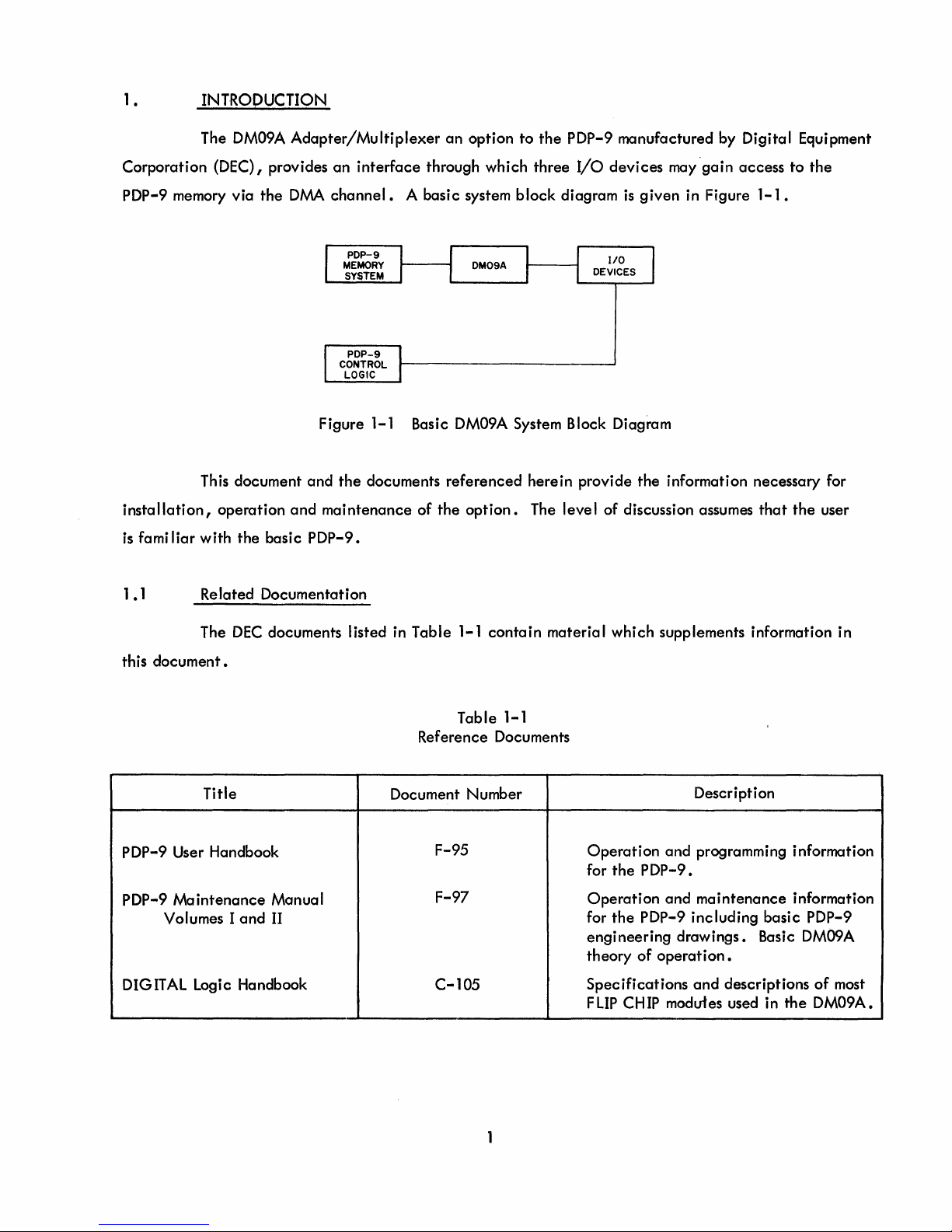
1 • INTRODUCTION
The DM09A
Corporation
(DEC), provides
PDP-9 memory
This document
installation,
is
fami
liar
with
via
the
operation
the
basic
Adapter/Multiplexer
an
interface
DMA
channel. A basic
an
option
to
through which
system
block
the
PDP-9 manufactured by Digital Equipment
three
I/O
diagram
Figure 1-1 Basic DM09A System Block Diagram
and
the
and
maintenance
documents
referenced
of
the
option.
herein
provide
The level
PDP-9.
devices
of
may'gain
is
given
in Figure
the
information necessary for
discussion assumes
access
1-1.
that
to
the
the
user
1 • 1 Related Documentation
DEC
documents listed in
this
document.
The
Title
P DP-9 User Handbook
PDP-9
Maintenance
Volumes I
and
Manual
II
DIGITAL Logic Handbook
Table
1-1
contain
Table 1-1
Reference Documents
Document Number
F-95
F-97
C-105
material
Operation
for
Operation
for
engineering
theory
Specifications
FLIP
which
supplements information in
Description
and
programming information
the
PDP-9.
and
maintenance
the
PDP-9
including
drawings.
of
operation.
and
descriptions
CHIP moduies used in
information
basic
PDP-9
Basic DM09A
of
most
the
DM09A.
Page 7
1
.2
Engineering Drawing References
II
be
Engineering drawings wi
referenced
using
an
abbreviated
code.
As
an
example,
drawing
D-BS-DM09-A-2,
[DM-2(2)] •
2.
2.1
Therefore,
2.2
No
additional
2.3
DMA
Adapter
Multiplexer
SPECIFICATIONS
Environmental
DM09A consists
The
entire
Iy
of
modu les
PDP-9 environmenta I spec ifications
Power Requirements
The option obtains a
power
supplies,
II
necessary
operating
power control
Physica I
The DM09A consists
entirely
of
modules which
Control,
of
the
apply
to
power from
or
fan assemblies
sheet 1 of
type used in
the
DM09A.
the
are
are
housed by two
2,
wi
II
be
referenced
the
PDP-9
centra
I processor.
PDP-9 power supply system.
necessary.
DEC
standard 1943 mount-
as
panels,
ing
tion
3,
2.4
control
2.5
thus requiring
INSTALLATION.
Controls
No
of
the
and
controls
PDP-9
or
and
PeITormance
The multiplexer
high
speed
and
thus
achieve
low speed of 3 iJS/transfer
the
speed range
applies
1 iJS/transfer.
10-1/2
Indicators
indicators
the
I/O
operates
a 1 iJS/transfer
to
permit
only
to
the
in.
of
mounting
are
associated
space.
with
devices.
at
two
speeds.
rate;
I/O
sufficient
data-line
DM09A. The PDP-9
the
I/O
devices
devices
settling
Placement of these panels
DM09A. The option
with 10
mHz
logic may request
is
is
entirely
with low speed logic should request
DMA
time.
channel
It should
and
the
be
remembered
memory require
given
in
Sec-
under
the
that
only
the
the
2
Page 8
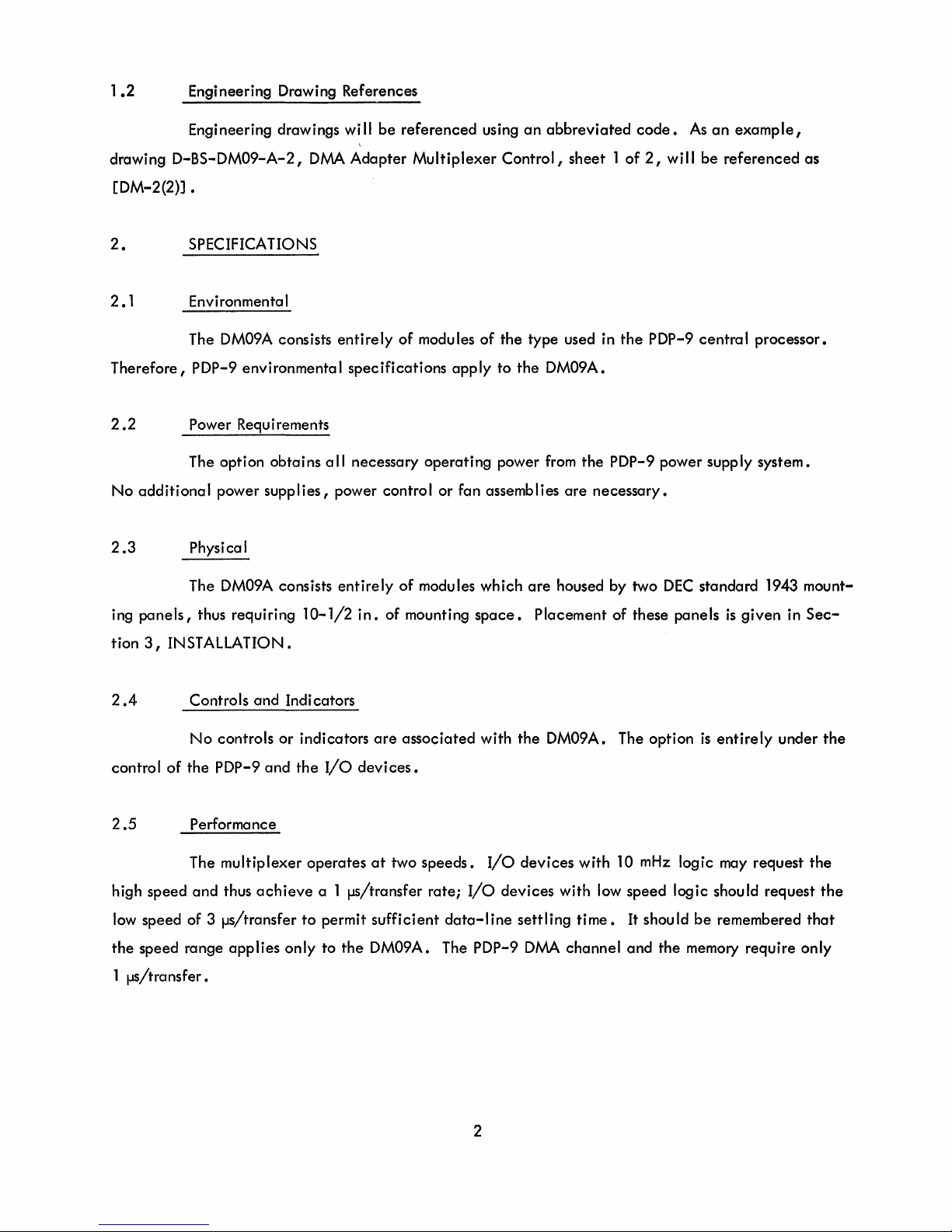
3.
INSTALLATION
prewired
Figure
3-1
Implementation
locations in
the
•
of
the
option
basic PDP-9
Figure
involves insta
cabinet.
3-1
The
PAPER
READER AND
OPERATOR'S CONSOLE
TABLE
Insta
II
location
RESERVED
FOR
DM09A
RESERVED
FOR
ME09B
TAPE
PUNCH
Ilation
ing
the
option
in
which
Diagram
modules
the
option
into
their
preassigned,
mounts is shown in
The following
Drawing
Number
D-CD-DM09-A-9
CD-D-DM09-A-10
CD-D-DM09-A-11
4.
4.
1 Basic
Channel
is
also
PRINCIPLES
A
basic
Transfers, of
contain
in
engineering
(Rev. A)
OF
description
the
PDP-9
that
section.
drawings
Title
Memory
Interface
DM09 Memory
Cabling
Inter-Memory
OPERATION
of
DM09A logic
Maintenance
provide
Interface
Cabling
DMA
Manual,
all
Interface
PDP-9 memory.
Interface
extension
bank.
Interface
and
operation
Volume
necessary
between
between
control
between
MM09A,
can
be
1. A detailed
interface
information.
Description
the
DM09A
the
DM09A, ME09A memory
and
MM09A
the
MC70B
Band C extended
obtained
from
and
extended
basic
memory
Section
DM09A
the
basic
memory
PDP-9 memory
banks.
3.8.3,
block
DMA
diagram
This
document
describes in
detail
the
operation
3
of
the
DM09A
DMA
Adapter/Multiplexer.
Page 9
4.2
Detai led
A
variety
of
transfer
type
combinations
are
possible with
the
DM09A.
To
avoid
excessive
repetition,
cyc
Ie
and
only
Doub
three
Ie
Certain
initialization
via
descriptions assume
Simi lar
operations
All transfer types
cing
with
a PDP-9
made
With
ready,
multiple
in which a
transfers,
When reading
referenced
DM-8(2) should
4.2.1
on
the
Power
When
be
Turn-On
the
types will
(Back
to
Back)-Fast-Output
DM09A
power
I/O
wi
ClK
operations
turn-on
device 0 is
II
result
pulse.
device
synchronization
the
signal flow
referenced
system
be
described
are
executed
and
when
can
be thought
interna
being
any
I DM09A control pulse
acted
other
of
Single transfers consist
is
synchronized
is
established
logic
descriptions,
tables.
for
is
first turned
In
specific
addition,
timing
on,
herein;
cyc
Single-Fast-Input
les.
regardless
upon.
device
is
acted
as consisting
to
the
PDP-9,
during
the
user should
DM09A timing
information.
PK
ClR
(power
All
of
time
of
transfer
train
reference
upon.
of
a number
states
or in which a
the
previous
refer
diagrams,
and
key
cycle,
type;
generation.
wi
II
be
of
"time
in
which
data
to
the
clear)
Single-Slow-Output
namely,
control
Transfer
made
to
I/O
device
either
data
states"
transfer
an
each
I/O
takes
transfer.
engineering
drawings
drawings DM-8(1)
pulses
arrive
at
circuitry
type
O.
commen-
device
place.
and
the
DM09A
is
control
The
operations
4.2.2
generate
system
logic
and
produce
performed
Clear
SYNC
Clear
SET
Clear
SET
Clear
DEV 0 CaNT
Clear
SLOW CYCLE A
Interna I Contro I
Following
an
internal
Ti
me
re lationships
is
operat i ng
AO
DO
PK
DM09A
•
PWR
are
0
Pu
ClR,
ClR
POS (power
as follows:
Ise T ra i n
ClK
(clock) pulses
control
are
pulse
illustrated
train
via
in Figure
clear
arrive
the
positive)
at
circuitry
4-2.
pulses
to
the DM09A control logic
of
Figure
The pulse
train
condition
4-1.
is
generated
the
and
control
are
used
whenever
logic.
to
the
4
Page 10
ClK
---+---JII
150fl
WI)05
A23
W005
W005
A23
A23
u
A D
PHASE PHASE
W005
A23
D
H
o
'VA
RIll
A21
F
U
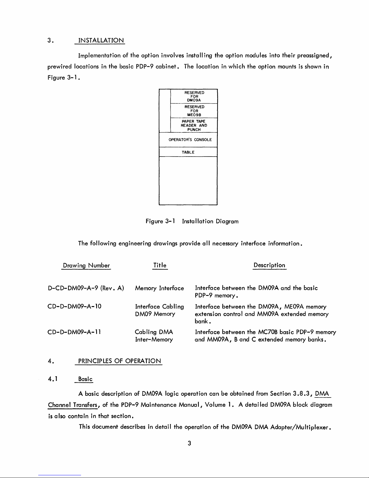
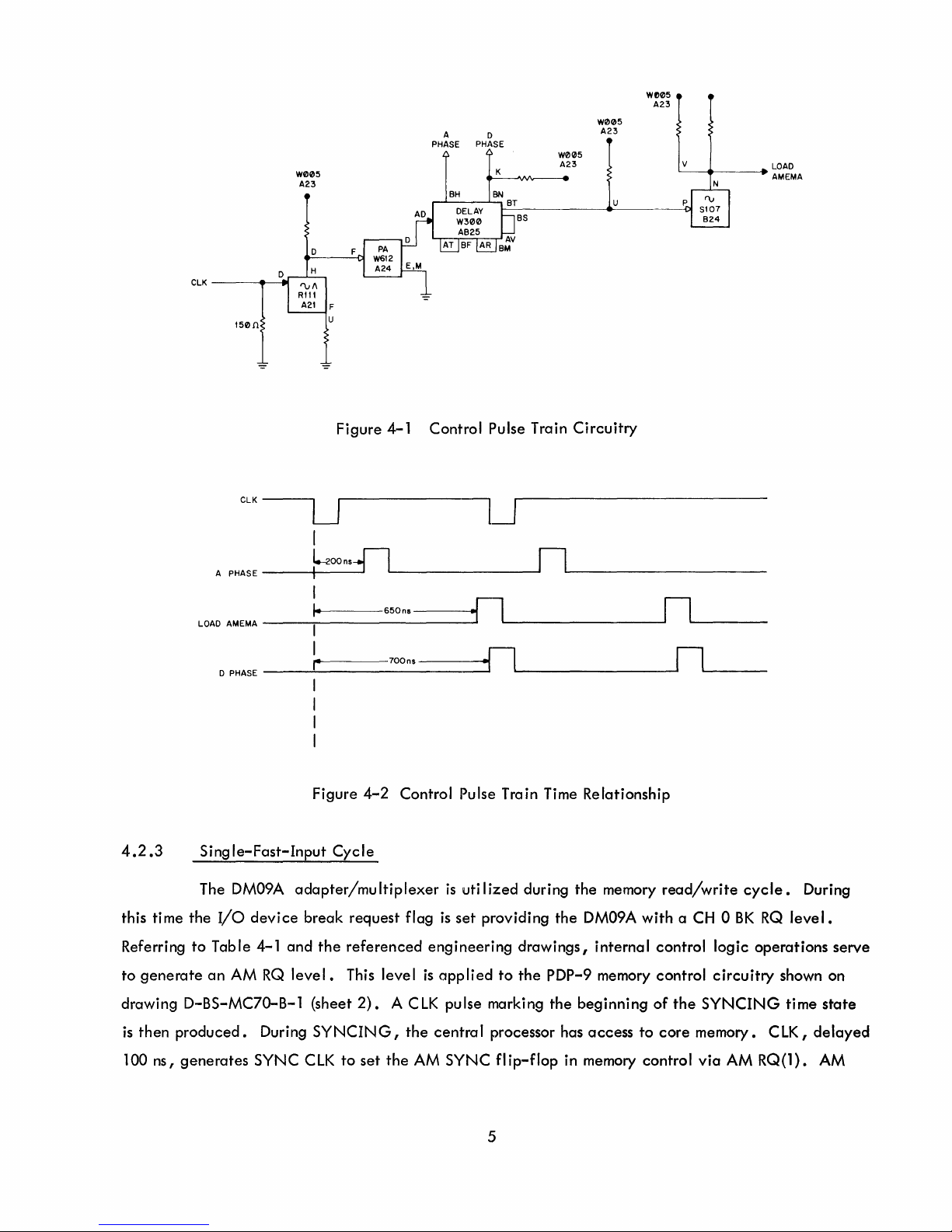
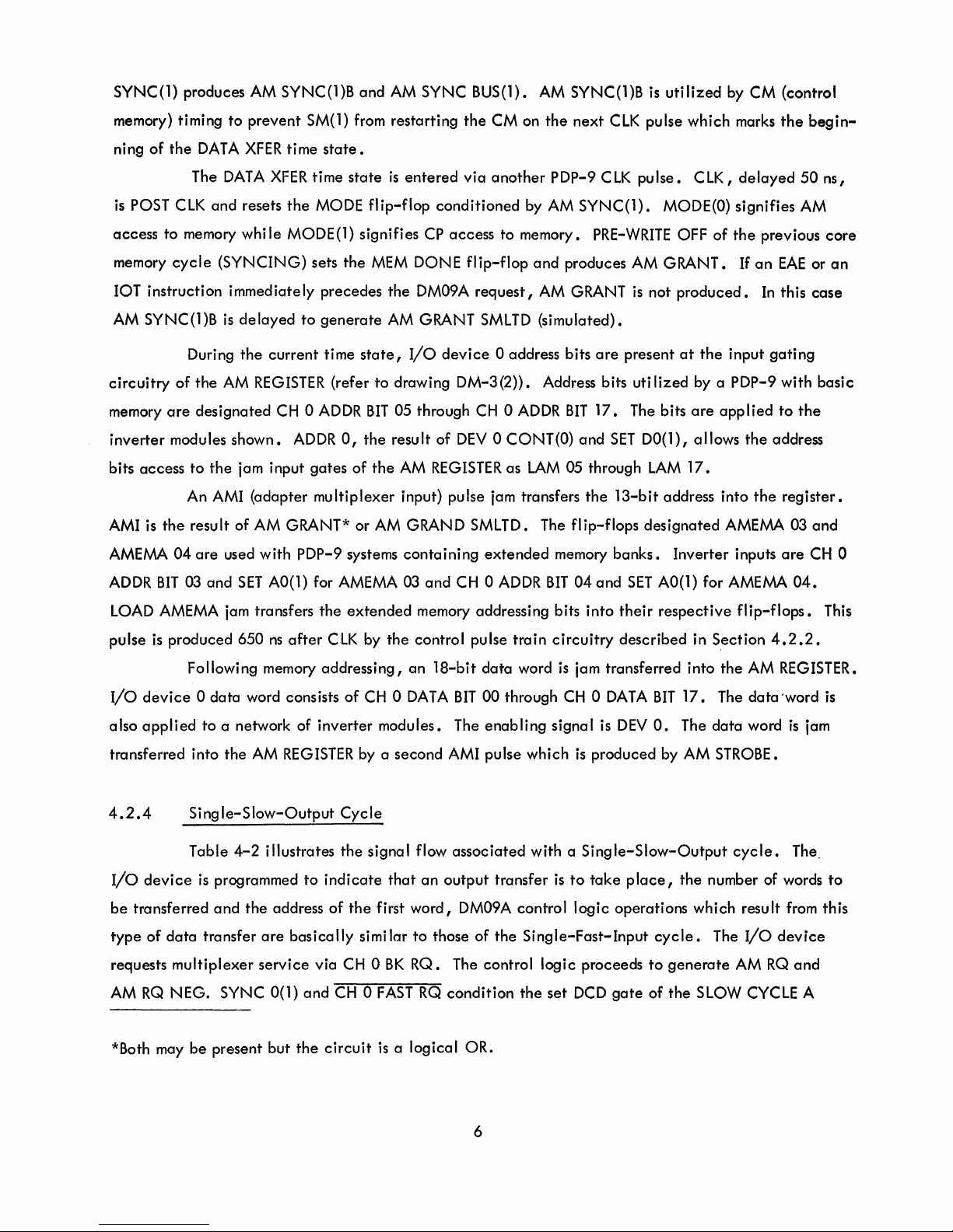
4.2.3
ClK
A PHASE
lOAD
AMEMA
D PHASE
Sing
le-Fast-Input
Figure
-----.U
I
~oons-n~------'n'---------
I
----:-1-----------'
__
!-14-------650ns----n
--'-
________
..
~----7oons----n
I
I
I
I
Figure
4-2
Cycle
4-1
Control Pulse Train
Circuitry
U
.....
----------'
----=.J
Control Pulse Train Time Relationship
L..
________
n
--I
n
~---
L..
__
_
this time
Referring
to
generate
The DM09A
the
I/O
to
Table 4-1
an
AM
adapter/multiplexer
device
RQ
break
and
level.
the
drawing D-BS-MC70-B-1 (sheet
is
then
produced.
100
ns,
generates
During
SYNC
SYNCIN
ClK
request
referenced
This level
2). A ClK
G,
to
set
the
is
flag
is
set
engineering
is
applied
pulse marking
the
centra
AM
SYNC
uti
lized
during
providing
drawings,
to
the
I processor has
flip-flop
5
the
memory
the
DM09A
internal
PDP-9 memory
the
beginning
access
to
in memory
read/write
with
a CH 0
control
control
of
the
core
control
cycle.
BK
RQ
level.
logic
operations
circuitry
SYNCING
shown on
time
memory. C LK,
via
AM
RQ{l).
During
serve
state
delayed
AM
Page 11
SYNC(l)
produces AM
SYNC(l)B
and
AM
SYNC
BUS(l).
AM
SYNC(l)B
is
utilized
by
CM
(control
memory) timing
ning
of
the
DATA
The
is
POST
ClK
access
memory
lOT
AM
to
memory whi Ie MODE (1) signifi es CP
cycle
instruction
SYNC(l)B
During
circuitry
memory
inverter
bits
are
modules
access
of
the
designated
to
An AMI
AMI is
AMEMA
the
04
result
are
to
prevent
XFER
DATA
XFER
and
resets
(SYNCING)
immediately
is
delayed
the
current
AM
REGISTER
CH 0
shown.
the
jam input
(adapter
of
AM GRANT*
used
with
SM(l)
from
time
state.
time
state
the
MODE
sets
the
precedes
to
generate
time
state,
(refer
ADDR
ADDR
gates
0,
the
of
multiplexer
or
PDP-9 systems
restarting
is
entered
flip-flop
MEM
DONE
the
DM09A
the
CM
via
another
conditioned
access
to memory.
flip-flop
request,
AM GRANT SMlTD
I/O
to
drawing
BIT
05 through
result
the
AM
device
of
REGISTER
0 address bits
DM-3(2».
CH 0 ADDR
DEY
0 CONT(O)
input) pulse jam transfers
AM GRAND
containing
SMlTD.
extended
on
the
PDP-9
by AM
and
produces AM
AM GRANT
(simulated).
Address bits uti
BIT
as
lAM
05 through
The
memory
next
ClK
ClK
SYNC(l).
PRE-WRITE
are
present
17.
and
SET
the
13-bit
flip-flops
banks.
pulse
pulse.
MODE(O)
OFF
GRANT.
is
not
produced.
at
lized
The bits
DO(1),
lAM
address
designated
Inverter
which
ClK,
of
the
by a
are
applied
allows
17.
marks
the
delayed
signifies
the
previous
If
an
EAE
In
this
input
gating
PDP-9
with
to
the
address
into
the
register.
AMEMA 03
inputs
are
begin-
50
AM
or
case
basic
the
and
CH 0
ns,
core
an
ADDR
pulse
also
BIT
lOAD
AMEMA jam transfers
is
I/O
device 0 data
applied
produced
transferred
4.2.4
I/O
device
be
transferred
type
of
data
requests
AM
multiplexer
RQ
NEG.
03
and
SET
AO(l) for AMEMA 03
650
ns
after
Following memory
word consists
to
a network
into
the
AM
of
REGISTER
Single-Slow-Output
Table
4-2
illustrates
is
programmed
and
the
transfer
address
are
basically
to
service
SYNC
0(1)
and
the
extended
ClK
by
addressing,
of
CH 0
inverter
modules.
by a
Cycle
the
signal
indicate
of
the
first
simi lar
via
CH 0
CH 0
FAST
and
CH 0
ADDR
memory addressing bits
the
control
an
DATA
second
flow
that
word,
to
BK
RQ.
an
RQ
pulse
18-bit
BIT
data
00
The
AMI pulse
associated
output
DM09A
those
of
The control
condition
through
enabling
transfer
the
BIT
04
and
SET
AO(l) for AMEMA
into
their
respective
train
word
which
circuitry
is
CH 0 DATA
signal
described
jam transferred
BIT
is
DEY
O.
is
produced
by AM STROBE.
with a Single-Slow-Output
is
to
take
place,
control
Single-Fast-Input
the
logic
set
logic
operations
proceeds
DCD
gate
cycle.
to
generate
of
the
flip-flops.
in S.ection
into
the
17.
The
The
data
4.2.2.
AM REGISTER.
data
word
cycle.
the
number of words
which
result from this
The
I/O
AM
RQ
SLOW CYCLE A
04.
'word
is
jam
The
device
and
This
is
to
be
*Both may
present
but
the
circuit
is a logical
OR.
6
Page 12
flip-flop
the
this
which
multiplexer
pulse jam transfers
is
and
set
in
by
the
the
the
positive
PDP-9,
device
going
transition
an
AM GRANT pulse
supplied
address
of
into
AM RQ
is
issued
the
AM
NEG.
to
produce
register.
Following
AMI.
This
is
logic
With
not
operations
input
necessary
in
transfers,
with
the
current
cycle,
to
produce
access
transfer
to
4.2.5
DM09A
DM09A
condition
time
state
DCD
gate
sired;
the
type
of
transfer.
Following
PDP-9
AM
SAl (sense
the
jam
these
bits
Doub Ie (Back
Signal
control
that
service
the
set
sets
SYNC 0 to
to
produce
computer
The A
STROBE
input
into
flow for
logic
is
DCD
responds
PHASE
further
amplifier
are
AM
DM09A
arrives
gates
of
the
AM
register.
to
Back)-Fast-Output
the
current
CH 0
requested.
gate
of
the
establish
RQ
and
with
pulse
of
control
at
the
DM09A. This
input) thus
the
AM
BK
RQ,
This
SYNC 0 flip-flop.
device
AM
AM
SYNCING
allowing
register. A second
transfer
CH 0
signal
priority.
RQ
NEG.
SYNC(l)
logic
Cyc
type
FAST
and
B.
1 sets
operations,
pulse
PDP-9
les
is
given
RQ
and
internal
The D
This
conditions
AM RQ
SET
signals
AO
similar
is
sense
AMI pulse
in
Table
CH 0
SLOW CYCLE
PHASE
and
generates
to
gated
with
amplifier
4-3.
RQ
IN.
pulse
the
the
PDP-9
those
CH 0
bits
is
produced
Initial
CH 0
A(O)
preceding
CH 0
that
CLR
of
Single-Fast-Input
RQ
IN
and
SA
00
through
at
this
time
signals
BK
produce
FAST
a DMA
SYNC.
sent
RQsignals
SYNC
the
SYNCING
CLR
and
cycle
This
SET
SA
to
to
the
0 EN
sets
is
clears
DO(l)
17
jam
the
to
1
the
de-
SYNC
SET
EN
set
another
CLK,
XFER 1 and
the
operations,
amplifier
AM reg ister •
place
O.
SET
AO(l)
DO
fl
ip-flop.
The following D
which
again
AM REGISTER. During
with
A PHASE,
because
AM RQ
the
to
jam
signa
flip-flop
The
PDP-9
SYNCING 2 time
and
syncing
AM
STROBE
bits,
SA
DATA
transfer
XFER
and
AM
SYNC(l)B
PHASE
maintains
SLOW CYCLE
I.
Because
remains
00
set.
produced
these
operations
arrives
through SA '17,
2 is
entered.
the
data
bits
generate
pulse sets
SLOW CYCLE A(O), a
A(O)
and
this
signal
AM GRANT
states
are
time
for
from
the
access
SET
of
the
CH 0
entered.
states
the
next
PDP-9
AO
second
SET
is
arrives
the
through
is
SET
DO.
BK
RQ
applied
at
The pulse
data
data
and
generates
cleared
word
DO
EN
SET
AO(l)
are
to
the
the
multiplexer
transfer
transfer
the
AM
and
into
the
which
characteristic
sti
PDP-9
jam-transfers
take
SAl
register
operations
conditions
and
SET
II
present.
AM
control
associated
pla.ce.
and
AMI,
gating
AM
register.
the
DO(l)
of
fast
Setting
SYNC
circuitry
address
with
the
thus a Ilowi ng
circuitry
simi lar to
The D
set
DCD
gate
produce
transfers.
fl
ip-flop
DATA
CLR
SLW
SYNC 0 is
SYNC 0 generates
prior
as
the
information
preceding
and
PHASE
syncing
the
sense
into
XFER 1 take
pulse
of
CYC
to
SYNC
DATA
into
the
at
the
the
end
of
the
current
ti me
state
c I
ears
SET
DO.
7
Page 13
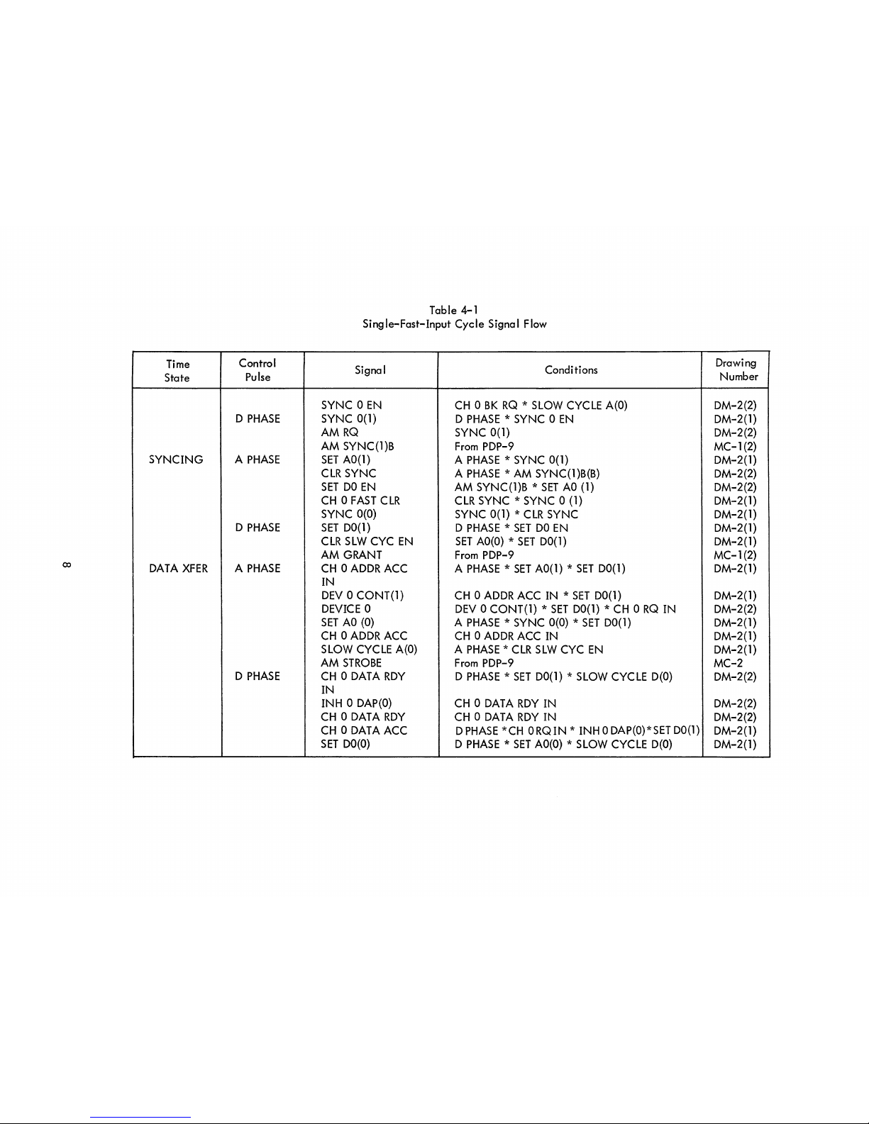
Time
Control
State
Pulse
D
PHASE
SYNCING A
PHASE
D
PHASE
DATA
XFER
A
PHASE
D
PHASE
Table 4-1
Single-Fast-Input Cycle Signal
Flow
Signal Conditions
SYNC 0
EN
CH 0 BK
RQ * SLOW
CYCLE
A(O)
SYNC 0(1)
D
PHASE
* SYNC 0
EN
AM
RQ
SYNC 0(1)
AM
SYNC(l)B
From
PDP-9
SET
AO(l)
A
PHASE
* SYNC 0(1)
CLR
SYNC A
PHASE * AM
SYNC(l
)B(B)
SET
DO
EN
AM
SYNC(l)B *
SET
AO
(1)
CH 0 FAST
CLR
CLR
SYNC * SYNC 0
(1)
SYNC 0(0)
SYNC
0(1) *
CLR
SYNC
SET
DO(l)
D
PHASE * SET
DO
EN
CLR
SLW
CYC
EN
SET
AO(O) * SET
DO(l)
AM
GRANT
From
PDP-9
CH 0 ADDR
ACC
A
PHASE * SET
AO(l) *
SET
DO(l)
IN
DEV
0 CONT(l)
CH 0 ADDR
ACC
IN * SET
DO(l)
DEVICE
0
DEV
0 CONT(l) *
SET
DO(l) * CH 0 RQ
IN
SET
AO
(0)
A
PHASE
* SYNC 0(0) *
SET
DO(l)
CH 0 ADDR
ACC
CH 0 AD
DR
ACC
IN
SLOW
CYCLE
A(O)
A
PHASE * CLR
SLW
CYC
EN
AM
STROBE
From
PDP-9
CH 0 DATA
RDY
D
PHASE * SET
DO(l) * SLOW
CYCLE
D(O)
IN
INH 0
DAP(O)
CH 0 DATA
RDY
IN
CH 0 DATA
RDY
CH 0 DATA
RDY
IN
CH 0 DATA
ACC
DPHASE
*CH
ORQIN * INHODAP(O)*SETDO(l)
SET
DO(O)
D
PHASE * SET
AO(O) * SLOW
CYCLE
D(O)
Drawing
Number
DM-2(2)
DM-2(1)
DM-2(2)
MC-1
(2)
DM-2(1)
DM-2(2)
DM-2(2)
DM-2(1)
DM-2(1)
DM-2(1)
DM-2(1)
MC-1
(2)
DM-2(1)
DM-2(1)
DM-2(2)
DM-2(1)
DM-2(1)
DM-2(1)
MC-2
DM-2(2)
DM-2(2)
DM-2(2)
DM-2(l)
DM-2(1)
Page 14

Time
Control
State
Pulse
SYNC
D
PHASE
SYNCING
A
PHASE
D
PHASE
DATA
XFER
A
PHASE
D
PHASE
Table
4-2
Single-Slow-Output Cycle Signal Flow
Signal
Conditions
SYNC 0
EN
CH 0 BK
RQ * SLOW
CYCLE
A(O)
SYNC 0(1)
D
PHASE
* SYNC 0
EN
AM
RQ
SYNC 0(1)
i
SLOW
CYCLE
A(l)
SYNC 0(1) *
CH 0 FAST
RQ * AM
RQ
NEG
-+
0
AM
SYNC(l)B
From
PDP-9
SET
AO(l)
A
PHASE
* SYNC 0(1)
CLR
SYNC
A
PHASE * AM
SYNC(l)B(B)
SET
DO
EN
AM
SYNC(l)B *
SET
AO(l)
CH 0 FAST
CLR
CLR
SYNC * SYNC 0
(1)
SYNC 0(0)
CLR
SYNC * SYNC 0(1)
SET
00
(1)
D
PHASE * SET
DO
EN
AM
GRANT
From
PDP-9
CH 0 ADDR
ACC
A
PHASE * SET
AO(l) *
SET
00(1)
IN
DEV 0 CONT(l)
CH 0 ADDR
ACC
IN *
SET
DO(1)
SET
AO(O)
A
PHASE
* SYNC 0(0) *
SET
00(1)
CH 0 AD
DR
ACC
CH 0 ADDR
ACC
IN
CLR
SLW
CYC
EN
SET
AO(O) * SET
D(l)
SLOW
CYCLE
A(O)
A
PHASE * CLR
SLW
CYC
EN
AM
STROBE
From
PDP-9
AMI
AM
STROBE + AM
GRANT
SAl
AM
STROBE * CH 0 RQ
IN * SET
DO(l)
SET
DO(O)
D
PHASE * SET
AO(O) * SLOW
CYCLE
D(O)
Drawing
Number
DM-2(2)
DM-2(1)
DM-2(2)
DM-2(1)
MC-1(2)
DM-2(1)
DM-2(2)
DM-2(2)
DM-2(1)
DM-2(1)
DM-2(1)
MC-1
(2)
DM-2(1)
DM-2(1)
DM-2(l)
DM-2(1)
DM-2(1)
DM-2(l)
MC-2
DM-2(2)
DM-2(2)
DM-2(1)
Page 15

Table
4-3
Double (Back to
Back)-Fast-Output
Cycles Signal Flow
Time
Control
Signal
Conditions
Drawing
State
Pulse
Number
SYNC 0
EN
CH 0 BK
RQ * SLOW
CYCLE
A(O)
DM-2(2)
D
PHASE
SYNC 0(1)
D
PHASE
* SYNC 0
EN
DM-2(1)
AM
RQ
SYNC 0(1)
DM-2(2)
AM
SYNC(l)B
From
PDP-9 MC-1
(2)
SYNCING 1
A
PHASE
CLR
SYNC A
PHASE * AM
SYNC(l)B(B) DM-2(2)
CH 0 FAST
CLR
CLR
SYNC * SYNC 0(1) DM-2(1)
SET
AO(l)
A
PHASE
* SYNC 0(1)
DM-2(1)
SET
DO
EN
SET
AO(1) * AM
SYNC(l)B
DM-2(2)
SYNC 0(0)
CLR
SYNC * SYNC 0(1)
DM-2(1)
D
PHASE
SET
DO(l)
D
PHASE * SET
DO
EN
DM-2(1)
SYNC
0(1) D
PHASE * SYNC 0 EN
DM-2(1)
-
a
AM
RQ
SYNC
0(1)
DM-2(2)
AM
GRANT
From
PDP-9
MC-2(1)
DATA
XFER
1
A
PHASE
CH 0 ADDR
ACC
A
PHASE * SET
AO(l) *
SET
00(1)
SYNCING
2
IN
DM-2(1
)
CH 0 ADDR
ACC
CH 0 ADDR
ACC
IN
DM02(l)
DEV
0 CONT
(l)
SET
DO(1) * CH 0 ADDR
ACC
IN
DM-2(1)
AM
STROBE
From
PDP-9
MC-2
SAl
CH 0 RQ
IN *
SET
DO(l) * AM
STROBE
DM-2(2)
SYNC 0(0)
CLR
SYNC
* SYNC 0(1)
DM-2(l)
CH 0 FAST
CLR
CLR
SYNC
* SYNC 0(1)
DM02(1)
D
PHASE
CH 0 DATA
RDY
D
PHASE * SET
DO(1) * SLOW
CYCLE
D(O)
DM-2(2)
IN
CH 0 DATA
RDY
CH 0 DATA
RDY
IN
DM-2(2)
AM
GRANT
From
PDP-9
MC-2(l)
CLR
SLW
CYC
EN
SET
AO(O) * SET
DO(1)
DM-2(l)
DATA
XFER
2
A
PHASE
SLOW
CYCLE
A(O)
A
PHASE * CLR
SLW
CYC
EN
MC-2(1)
CH 0 ADDR
ACC
A
PHASE * SET
AO(l) *
SET
DO(l)
DM-2(1 )
IN
DM-2(1
)
CH 0 ADDR
ACC
CH 0 ADDR
ACC
IN
AM
STROBE
From
PDP-9
MC-2
SAl
CH 0 RQ
IN * SET
DO(l) * AM
STROBE
DM-2(2)
D
PHASE
SET
DO(O)
D
PHASE * SET
AO(O) * SLOW
CYCLE
D(O)
DM-2(1)
Page 16

5.
ACCEPTANCE
TEST
PROCEDURE
with
6.
Acceptance
the
DM09A Tester
Minimum margin
MAINTENANCE
testing
at
of
both
specifications
the
normal
Trial
1
2
3
DM09A
operating
DM09A-O
DM09A-O
DM09A-O
for
+10V
+6V I
option
conditions
Test
rack A and
Margin
-6V
consists
Aggravation
Condition
None
Margin
Margin
rack B are
-15V
+4V ,
of
executing
and
the
rack
rack
-4V
Test
voltage
A
B
listed
Procedure
margins
below.
DM09A-O
specified
below.
6.1
apply
6.2
6.3
to
General
The
the
DM09A
Delay
Adjust
Module
Table
general
option.
Adjustments
the
R302
Complement
6-1
lists
maintenance
Delay
the
at
module
procedures
A27
according
complement
described
to
the
of
the
in
the
data
DM09A
PDP-9
given
option.
maintenance
on
engineering
manual
drawing
also
DM-2(2).
11
Page 17

Table
6-1
Module Complement
7.
DEC
Type
B169
B213 Jam
R002 Diode
R111
S107
S202
S203
Module
Inverter
Diode
Inverter
Dual
Triple
Type
Flip-Flop
Cluster
Gate
Flip-Flop
Flip-Flop
S603 Pulse Amplifier 5
W005
W300
Clamped
Delay
Line
Loads 3
W612 Pulse Amplifier
R302
*Contained
in
ENGINEERING
One-Shot
the
basic
DRAWINGS
De
lay
processor
spare
Quantity
Recommended
17 2*
14
2 1*
12
2 1*
7 1*
1
1 1
S
1 1*
parts
kit.
Spare
1*
1*
1*
1*
Quantity
Drawing
DM-2(1)
DM-2(2)
DM-3(1 )
DM-3(2)
DM-4(1)
DM-4(2)
DM-5
DM-S(l
DM-S(2)
Table
Number
)
7-1
lists
the
DEC
engineering
Engineering Drawings
DMA
Adapter
DMA
Adapter
AM Register
AM Register
Cab
Ie
Diagram BS-
Cable
Diagram
Module Uti
Multiplexer
Multiplexer
BS-DM09-A-3
BS-DM09-A-3
BS-DM09-A-4
Iization
DM09A Timing Diagram
DM09A Timing Diagram
drawings
Table
associated
7-1
Title
Control
Control
Sheet 1 of
Sheet 2 of
DM09-A-4
Sheet 1 of
Sheet 2 of
MU-DM09-A-5
TD-DM09-A-S
TD-DM09-A-S
with
the
BS-DM09-A-2
BS-DM09-A-2
2
2
2
2
Sheet 1 of
Sheet 2 of
D"A09A
option.
Sheet 1 of
Sheet 2 of
2
2
Revision
2
2
J
J
B
B
0
A
H
0
0
12
Page 18

D
c
B
A
8 7
CH ¢
ADDR
~ee
LN
H..J
ST
CH ¢
ADOI'<
ACC
5T
SET
AI(I)
K
S=:T 0 1(1)
L
HJ
6
PWR
C L R
POS----'---t:I--r==-:----=.-f--L--------O'-i'=-.!-='-i-...l-------C>J--i==-'--'::.....;:...l
D
PHASE.
S=:T
A ¢
(rf;)
SLOW
c.YCl:E:Otf),
=:
A
PHAS.E
'.3ET D ¢(I)
PWR
CLR
D
PHASE
CLR
SYNC
.=:..(:{;?3:}---+------'.N,,-o!8j--+--------'D~C8:I
:E.N
'SYNC
I
(I)
'SYNC
2..(I~
8
7
\...
6
5
4
3
2
CH I ADDR
Ace
IN
CH 2 ADDR
Ace
IN
1'\
D
CH I ADDR
Ace
CH
2.
ADDR
Ace
CH ¢ DATA
Ace
CH I
Rq
IN
wl1Jr/is
CI9
58"
A2
(I)
SET
D2(1)
Ace
eN
2
RQIN_~~~
SLOW
CYCLE 0
(I)
eLR
W~rj5
C.19
CH
'2. F
.....
ST
C.LR
CH ¢ OAT A RDY
HJ
CH I DATA
RD'I
IN
CH 2
D"TA
RDY
IN
SHA¢(;)
SET
D <)(1)
CH
if;
ADDR. ACe.
~N
CH I
"'-DDR
ACC
IN
CH e
ADOR
Ace
IN
5
DPHASE:
.s
T
;:,
T
SLOW·
CYCLE
0(1)
K
A PIfAS£'
---1>Ei;;;:"\--;;>f)<:]
CH
2.
DATA
Ace
c
PWR
CLR
POS
--;;:O-=;=-''-=--=T-'
/I
PHitS~
fl
M.
RQJi
EG.
CH i
CH
2
B
t----------...-------+-----<O
CLR
SLW
eye
EN
3
A
2
BS-DM09-A-2
Sheet
1 of 2 DMA Adapter
Multiplexer Control
13
Page 19

Page 20

D
c
B
A
',7?5
r 2.(.'
8
CH
CH ¢ DATA RDY
IN
H F
C H 0 RQTN
--q~("V
IS/()7
824
8
7
6
•
EN
~5ET D ~SET
D Z
EN
I--
__
--'-K~
..
I---~~N
AM
SYNC(i)e.CB')
L
SYNC.
2.
EN
ROY
K
L
SYNC
2.
(¢)
A.
PHASE
SnlC.
2.
(91)
7 6
SYNC
¢
(I)
SYNC
1(1)
5
p
5
M
F
K
F
H
A
PHASE
(B)
4
I\M
RQ
AM
RQ
NE~.
AMI
-=
SAL
A
D
4
3
CHQRQIN
DEV ¢ CONTROL(I)
DEV
SET
0 i/'J(I)
CH 1 RQ
IN
\
CONTROL(I)
SE.T
D 1
(I)
A2d
LOflD
/lMEMA
CH Z RQ
IN
DEV 2 CONTROL(I)
SET
D2.(I) U
PK
CLR
I!>¢A
3
2
W¢¢5
A2?
I
D
1M
-=
DEVICE
Q
U
/\
V
DEVIC.£ \
C
K
/\
L
/1
M
GRIiNT
SNiLTD
1M
/1
M S Y N
C.
(I) B
--_£PI.2;sJ
v
PWR
ClR
pas
2
liDJUS
r
/t/J/I
GR/jf'{T
SMLTD.
TO
occuR
AT
AM
GRliNT
TIME.
B
A
BS-DM09-A-2 Sheet 2 of 2
DMA
Adapter
Multiplexer
Control
15
Page 21

Page 22

D
C
8
A
8
7
SA0£!
SA I
CH 0 DATA-BITll0
DEV
~
CH
I DATA-BIT.0'.0'
DEVI
CH
2 DATA-BIT¢¢
DEV2
M
C
::-
NOTE:
loon,
tw,
lOt,
TERM I NATORS
TO
GROUND
MUST
BE
PUT
ON
SA00
THRU SA
17.
8
SA
12
SAl
CH
0 DATA-BIT
12
DEV 0
CH
I DATA-BIT
12
DEV
I
CH 2 DATA-
BIT
12
7
6 5
3
2
D
c
M
loon
B
M
c
c c
A
6
5
4
3
2
BS-DM09-A-3 Sheet 1 of 2
AM
Register
17
Page 23

Page 24

o
C
B
A
8
CH
\)
ADDP.
BIT03-
SET
A(11)
CH I
ADDR
BIT 03
SET
AI (I)
CH
2
ADOP.
BIHl3
CHiZlAOOR
BIT
ADD!?
JIJ
C"
IAOORBITI4
ADDIl
I
CH
2 ADOP
BIT
14
AODR
2
8
7
E 0 E D P,.,.....,..------,...-,
M
LAM
14
M
CH
I
ADD!?
BIT
0'4
CH
2AooR
BIT
04
CH0AODR
B!T
15
C,.,I"'OOR
BiT
15
CH2ADOR
V
BIT
15
C
-=-
LAM
15
7
':'
BIT
16
CH2AOOR
BIT
lEi
CH
iZlAooR
BIT
05
CH,AoOR
BIT
05
CH2ADDR
V
BIT
05
M
-=-
LAM
16
BIT
17
CWI
AOO~
BIT
17
CH 2 ADDP
BI
T 17
6
6
LAM.0'5
LAM
06
CH
0ADoR
BIT
1216
CH
IAOoR
BIT
06
CH 2 AOoP
BIT
1216
C
M
-=-
-=
LAMI7
c
5
4
LAM
(67
LAM
I2IB
CH 0 AODP
CH
0AoOR
CHrllAODR
BIT07
BIT
08
BIT
0'9
CHIAoORS
CH
I AOOR
CHIAOoR
BIT
07
BIT
(lj8
BIT
09
CH 2 AoOR V
CH2
AODP
CH2ADDRV
BIT
07
81T
£18
BIT
1'19
C M
-=
-=-
W005
A23
H
DEV
CONTROL
(0)
U
1\
v
5
..
3
LAM
09
LAM
10
C
DEV
2CONTROL(0)K
3
CH 0 AODP
BIT
II
CH
IADDP
BiT
II
CH 2 AOOR V
BIT
II
LAM
II
c
LAM
12
M
ADDR
2
2
2
BIT
13
CH2ADDRV
BiT
13
D
LAM
13
C
c
B
A
BS-DM09-A-3 Sheet 2 of 2
AM
Register
19
Page 25

Page 26

8
7
o
c
8
A
8
7
CH
0 BK RQ
RQ
IN
FAST
CH 0 FAST
CH
I BK
RQ
RQ
IN
DATA
FAST
RQ
CH I FAST
CH
2 BK
RQ
RQ
IN
ADOR ACC
DATA ACC
FAST
RQ
CH 2 FAST
CLR
6
WC/J31
DC/J4
W031
012
6
CLK
AM
SYNC(I)B
AM
RQ
AM
STROBE
AMEMA
134
(0)
CH
0
6K
RQ
CH
I/J
RQ
IN
CH 0 FAST
RQ
CH
I BK
RQ
CH
I RQ IN
CH I
FAST
RQ
CH
2 BK RQ
CH 2
RQ
IN
CH 2 FAST
RQ
AM
(/)9 (il
l\il
II
12
13
14
15
16
AM
17
(Il
5
W¢33
G795
AI/J5
AI5
"*
•
E
·
H
I(
M
•
p
•
S
T
•
V
SA
¢i/J
QlI
02
03
¢4
(/15
06
0
7
SA
(/18
4
SA
09
1(/1
II
12
13
14
15
16
SA
17
"*
USED
FOR
TERMINATION
ONLY
NOT A
CABLE.IOPTIONAL)
W031
013
*
Wy)33
A04
5
AM
i/JC/>
(I)
I/JI
1/J2
03
04
05
1/J6
07
AM
08 (I)
AM
C/J9
(I)
llil
11
12
13
14
15
16
AM
17
0)
W!Il31
Af/)3
~(IT'
E
-
H
~K
-4M
-4p
S
~T
-4
~,V
'-'
W031 W031
D¢2
0¢6
(IT'
W031
010
(IT'
AM
00
(I)
01
-4
E
-4H
(t5'
E E
02
¢3
04
05
06
07
-41(
-4""
-4p
-4S
.-
T
-4
V
H
H
I( I(
M M
P P
S S
T T
AM
(1)8
(I)
V
~
(CH
I)
W¢31
0¢7
(IT'
E
H
K
M
P
S
T
V
(CH
2)
W031
011
(15'
E
H
K
M
P
S
T
V
4
"-"
'--'
(CH~)
(CH
Il
(CH 2)
NOTE:
PINS
C,F,
J, L,N,R,U
ARE GND
FOR
ALL
WQl31'S
AND
Wr/J33'S
3 2
D
c
B
A
3
2
BS-DM09-A-4 Sheet 1
of 2 Cable
Diagram
21
Page 27

Page 28

D
c
B
A
8
7
iWQ)cz,-s-i<1
\1'1031
,ClIO
: C(;llI
I I
C~(,i'DP.-f'.b-;-
rj;¢
I
DI
~
!
~I
~----~~~
r:P
2..
-,------:-.1
\-\
\<:
r:P3
----;------~.
M
¢q.
----;-------=-~.
P
CP5
-;----+-'~
¢~:
~
I T
(j)'7
----;-----ec...:.~.
t v
Crl
q:,
'2>AT/,-
BIT
¢5
----;-I----ec...:.,..
Crl
I
i'-'ODR
8\T
g\~
rjJ4
8
L
___
-.-l
W¢31
C¢7
o
I
FI
'E
•
\-\
·
K
·
1:'\
?
""!
5
-;----+'-:,-.1
~
01
\"
---.,----+-.,-41
•
"'!
v
1 I
L
___
-l
7
eH
¢ OAT/'-
611
¢g
\$
II
IZ
I~
l't
IS
10
CI-I
r:/J
DAIA
'ell
1/
CH I
P\DDR
\3\\
¢'"
I<:D
II
12
\3
I"\-
IS
lCO
CHI
",DD~
'8\\\'1
6
I
~----~~.
V
~,----~,:-./
.
:W<P¢5
!
L~I~
__
J
L:
'0
~----~I:-.I
•
\'\1 E
--;------I~
•
NI
\-I
?l
\<:
-:-----·R~I:-.I
:.
os:
p
~----'-=I:-.I:
II
->
-,---_'""1
Ii.
UI
T
--'-----,41
•
'I!
v
--'-----:-./
-
L
___
J
6
CH
(/>
I\DDR
61T
¢~
I
07
CI-\ ¢ I>.D'OR
8\1
¢s
CH
2.
DATt>.
B\\
(/jet>
dJl
CP2
O~
cPo,
dJs
¢t:C
<:$'1
CI-IZ
D"-,'"
BIT
¢'8.
5
W031
C¢3
o
·
'E.
·
\-\
•
fW¢¢5"V
""d31
1
CI
<0
1
V'
'P
I I
C¢~
I
'01
0
------,----+=~.
1';.1
'E
------,-----,....1
~.
FI
\-I
----.,.----'"'1
~.
1-11
K
~--Flc.f·
JI
M
---7----+='-;I~
•
\'\1
P
-;----~I~
•
Li
5
----'-----41.
Ml
'
---:-::---7-401
•
I
Nt
~
I I
L
___
...J
·OPTIONAL
CLAMPED
LOADS.
5
4
eH
q;
r>.DDR
SII
cjJ9
Irb
II
12-
I~
l't
IS
\CO
CH
C(:J
I\DDR
'CIT
\'7
CH
2.
DF>.'(>"
BIT
09
1
Iq,
II
\"2-
j
14-
IS
I<D
c.1-I2.
DA,\A.
BIT
\'7
4
iwi>"¢S-"'i
W~31
ICI~
I
cal"\-
!
;'
E
----;----+-''-41
•
1-\
\'\
-,-----,...
M
p
3
eH
I
DI>.T'"
'ell
¢ci>
(/:;\
cD?..
¢~
¢q
cps
¢ro
¢.,
CH I D"'\"
'8.1\
¢'6
CH
2.
ADDR
811
rj,7:!,
iJq
¢s
r/>r::a
¢..-,
CH L ",bOR
'5\,
¢>~
3
W~31
CII
D
•
E
.
1-\
CH
\ '0"',(>...
So\\"
¢9
t
10
II
1'2..
I~
\4
IS
\<0
CI-\
I D(>...'''''
'C\\
\ro,
CH
2.
I>.'O'OR
'CIT
¢?>
Icf;
II
12-
\~
Ic\-
It:>
\~
CH'C
I'\\:>DR
'61\
\I
2
2
wz,¢"5-ot-,
f!t3:
lei",
:-=%
I~V-ol
B
•
.I.!
I
e--'V\-
I
1_
1
!
31='1
•.
~:
i
....vv-:si
M
1
I·
I~-:-I";.
:~'Ji
t<"
II:
P
~---l
"'.
I
\-11_
:~0:
'
i
K:
1 I
iwalc;i>5
i
LC"':'~_J
lvVarQ5s'il
I
C.IS
I
will
3 I
I 1
c..1'Z...
I
LI
D
I •
I
M!
'to
-,-I----*-'-~
-
1
NI
\-j
I
I
?I
'"
~----+---,..
•
______
..
R_:~
M
sl
'?
-...,------<l.=..~
T:
So
1
u:
T
--+1--_+---:-.1
•
1
vi
v
I
I·
L
___
~
D
c
B
A
BS-DM09-A-4
Sheet 2 of 2 Cable
Diagram
23
Page 29

Page 30

D
c
B
A
8
7
2
3
4 5 6
7
8
11IIP
le33
1933 WG'.33
W1J33
8213
~213
B213
AM
AM AM
au
·1l2
·111
SA SA
AM
AM
~g~~.
11-2
9-17
0-8
MEM.
9-17
-
AM
AM AM
·91
·93
115
B169
B169 B169
trl69
8169
B169
BI69
B169
LAW
LAM
~MEM,A
LAM
LAM LAM LAM
.~Jl
.02
03
.04
llS
.9S
.S8
I
i
B
AMl
,~
LAM
LAM
LAM LAM
LAM
LAM
.91
·S3
0485
as
.87
.87 .89
2
3
4
5
6 7 8
f+--
CH9
CH
1
.
C 1
0m
8-8
ADBDI
RT
I
DATAl
OAT
A I
ADOR I AODR
I
BIT
BIT I BIT BIT
9-17 I
·0-8
9-17 I 3-8 9-17
om
I
A~~~
9-171 3-8
W031
W~31
11131
o
AM
AM
CONTRO
SPARE
9-8
9-17
SIGNAL
SPARE
I
(NEG)
(NEG)
i I
I
I I
I
i I
8
W0]31
W031
11131
CH
I
All
AM
.8-8
9-17
(NEG) (NEG)
I
I
CONTRO
SIGNALS
I
I
I
I
7
6 5
4
3
2
9
10
II
12
13
14
15
16
17
18
19
20
21
22 23
24
25
26
27
28
29
30
31
32 33
34
35 36
37
38 39
40
41
42
43
44
8213
I
~213
11213
6213 6213
8213
16795"
1612
R8IJ2
RIll
Sl8 I
8213
RIll
1lIII5
IRI2
,-
15603
7
CLR
~
AM
AM
'"
V
A21Y
~
A23F
~
GRNT
GR.NT
f-----
r{~:c
A~
)~Y~~
F=-
-
coo:::
S
SMLT[
15MLT
1'"
V
AM
Ali
AM
AM
AM
AM
AM
~
AMI
AlaM
~
A2SD
n
ji8
I·e
12
14
16
f---
SYNC
1
RQ
f---
~
P
~
V
ONTROl
f---
(Il)
~
FROM
~IBS_
I,
~HASI
r-.
2Jl
1S..
~
A
A
EMORY
f-----
AISH
f---
SPARE
f---
f--
~
V
lEVEL
(B)
>--
PHASE
f---
R.
TERM.
f---
~.
>--
AM
All
AM
All
AM AM
f---
2
f---
f---
~
V
I
111
S~I
>--
E
$7
·99
13
IS
17
AI6F
f---
I
f-----
I---AIBR~
~~h~
I
J----
~
~
1/
i
BI9l
AI7L
S24N
8169 B 169
8169
B169
~IB9
B169
B169
R1S9
R169
RIll
B213
R213
R213
g.l!a2
8213
15107
I--
52(02
R
~?Q2
R
/1'.
I
CLf'.
V
""
B19V
Ba~N
SLW
V
I
LAM
I-A
18K
>--
iAMEMA
I-
-
eyC
~
LAII
LAM
LAM
LAM
LAM
LAM LAM
LAM
ADOR
~DDR
OEV I CE
SLOW
OEV!
~3
EN
.sa
1·9
1;9
12
12
14 14 16 16
J-----
.8
2 1
BZIIl
I;WN
CYCLE
f--
CONTROl
+-----
V
~
f---
A
CLR
I~~IN
0
SLW
A18L
8Z11V
f--.....-
f---
B2B11'
J-----
V
~
I
L6
2"D
PHASE
eye
f---
EN
J----
B21L
iAMEMA
~MEMA
SLOW
f-
-
+-----
V
~
LAM LAM LAM
LAII
LAII
LAM LAM
LAM
LAM
AODR
DEV I CE
OEV
ICE
rGAR~
CYCLE
OEV
I
CLR
~
A17H_
~
134
D
SLW
.89
II
11
13 13 15
15
17
17
1 8 2
~
f-
-
CONTRO
/
~
a21V
CYC
EN
9
10
II
12
13
14
15
16
17
18 19
20
21
22
23
24
25
26
27 28
29
30
31
32
33
34
35 36
37
38
39
40
41
42
43
44
R
11
~?"7
~?A7
<:'?IJ? S?A?
S?.A?
R
R111
Cll2T
C23l
r.II'V
-[)?1S
DISF
C.\lSS
C.z.3H
CH
2
+--
C.\lST
Cl3N
I
~YNC
SET
0
II
I2N
.8
EN
SET
SET SET
1---+----1
09
0:1
A 1
SYNC
SYNC
...&25E_1-
C26P
2
I
~~:~
fsy:~
CH:S
CHI
CH2
DATA I DATA
DATA
C1.S'F
jSVNC-E
BITS BITS I BITS
CI.D
CH.8
CH 1 CH
2
I
AODR ADDR : AOOR
BITS
BITS
81TS
OISR
SPARE
!-~Y~~
'-SH,,..,;Dt--_-+_-t
__
t--_-+_-+
C25P
t--
C27E
_
DATA I DATA I ADDR I AOOR
BIT I BIT
BIT
BIT
.9-8
9-17 3-8 9-17 S3-
17
113-17:
83-
17
:88-14
811-14
.14I--::-
B2
'""7-=-0+----I
I
I
~.;,.;1i22;.,.tK.-I---+---l
j-.;B;':27~R+-----1
1-
0
,,--24_0
-+-____
DI9
F
024H
024L
SEl
SET SET
A
Jd
A2
W031
w031
1iS31
'195
W612
W612
W612
'6~2
W812
1612
RIll
S6,0~
RIll
s-6]J3
RIll
S6~31S203
CH
2
All
SPARE
.9-8
I
(NEG)
CHji
AOOR
ACC
CH 2 CH 1 CH 8 CH 2 CH
I
ADOR AODR
US-T
DAn
DATA
ACC
ROY
CLR
CLR
ACC
CHJd
CH0
CH¢
INH
AODR
ADOf'.
D1SR_
DATA
,-OEV
.11.
D19f'.
[6
~~C
ACC
P.oy
IN
DAP
IN
IN
CH
1
CH I CH
I
INH
CH
f---+---+--t--+---+--I
ADDR
ADDR.
D11F_
DATA
I-0~V
L
D2.¢F
1
9~~7
~~m~i~E~Et
S~ARE
~~C
ACC R.DY
IN
DAP
(NEG): ' TERM
. I IN IN
I
I
!
CH
I
eHS
CH
2
·1
CH
I
eH.8
CH
2
I
ADOR
DATA
OATA
FAST I DATA
DATA
CH
2 CH
2.
C H
2.
INH
I I
ACC
ROY
ROY I CLR
ACC
ACC
ADDR
ADDP.
0171L
DATA
I-
DEV
L
D20R
2.
I
I
~~C
ACe
RDY
IN
DAP
IN IN
NOTE!
FOR
MODULE
COUNT
SEE
A_PL_OMS9_A_5
6
5
4
SYNC
1
DEY
2
ONTROLf...£26L
C27P
*"
OPTIONAL
MOOULES.
3
2
MU-OM09-A-5 Module Utilization
25
D
c
B
A
Page 31

Page 32

8
D
c
B
A
8
COMPUTE.R
BASIC
C.YC.LE
A
PHASE
PULSES
(120
NS)
(INTE
R NAL
DNl09A)
o PH ASE: PULSE S
(leO
NS)
(INTERNAL
DMO'7I1)
C.HX6KRG,
(FROM
DEV
X TO
DM09A)
SYNC
X
(INTERNAL
DM0911)
7
6
~
I
SiNGLE.,FAST,iNPuT CYCLE
fll
SYN
IN
5
4
Ii
SiNGLE,
SLOW,
OUTPUT
CYCLE
0
SYNCING
au y
3
"liST
CLEAR\,
ADDR
ACCEPTED
X
~
\ \
~"1------------------~===~~_-'
__
-_3
___
~~~_-~~'----------------------r~~_~~
________
~/~I
a
~Ow
CYC.LE:
(0)
·CHX
BK
RQ
(-3)-D
PHIIS!
------~
LJ
AM
'3
YNC (I) B
-A
PHASE
2
AM
RG.
(FROM
DIVlO
9fl
TO
MEMORY)
SYNCX-I,,_,
,.r-SYNc.x_o
-1:
:r'_
_________________________ ~~'_ ______________________________
~~'---------------------
::
I I I I
~
, t I I I :
200
NS
--:
r--
200NS--.
---
400
NS
-i
'--
MAX
:r----\
MAX
;!----\~
________________________________
M_A_X
____
~/~'
---------,L-
______________________
_
AM SYNC
(ll8
(FROM
MEMORYTO
DM09f/)
--------cc
YNC
x (I) -
fI
PHASt::
ss:rll
x I
(INTERNIlL
DNl09A)
CH
X
FAST
RQ
(FROM
DM091l
TO
DEV
X)
CHX
RGI
IN
(FROM
DEV
X TO DIVI091i)
SET
D X
(INTERNAL
DM091l)
SYNC
x(o)·
StT D X(I)·/9
pHASE
SLOW
CYCLI::
(INTERNAL
DM09A)
SHM'.M'Y"""'~
SLOW
CYCLE
(0).
SET
Ii
)«(O)·D (
CH
X
FA
5T
RQ
(-3).
SYNC. X
(I)
·AM
RGl--~
PHASE
,
--------------------------------------~
1.9
MS
Jl/
7
6
5
4
3
2
TD-DM09-A-8
Sheet
1 of 2 DM09A
Timing Diagram
27
D
c
B
A
Page 33

Page 34

8
D
c
B
A
8
C:CMPlF-ER
BASIC
CYCLE::
A/II
GRANT
(FROM
MEMORY
TO
DIfl09A)
AM
STROBE
(PROM
MU;70RY
TO
DM091i)
flDDR
ACCEPTED
(er/x)
(FROM
DMo'?h
TO
DEV
X)
DATA
READy
(CHX)
(PROM
DM09A
rODEYX)
CATA
ACCEPTED
(CHX)
(FROM
DMO
914
TO
DEV
X)
C H X
ADDR
(PROM
D.£V X
TO
DfYl09A)
CH
X
DATA
(FROM
D£V
X
TO
DI'II09/1)
SENSE
/IMPS
(FROM
MEMORY
TO DM091l)
AM
LOADED
(F
ROM
DII'I091l
TO
On
X ¢
MEMORY)
CH
X FI7ST
CLU~R
(Ff:eofVI
DfYlO
91i
TO
DEV
X)
7
6
5
4
~
SINGLE,
SLOW,
OUTPUT
CYCLE
0
SYNC-tNG.
8 y
U
(120N5)
U
(120
NS)
__________
-r'~SET
D X
(I).
SET
II X (i) • A
PHIlSE
U
(320
NS)
u
___________
---1~SLOW
(yc.LI::
(¢)'SHD
x(l)·
D
PHASE.
U(320
!'Is)
___________
---1~CHX
RQ
IN
(-3)·
SET D X(I)·p
PHASE
lJ(320
NS)
u
u
u
3
r
DOUllLE
(BIlCXTO
BACX),
"AST,
O~TPUT
CYCLES
-1
SYNCJ"G. 1
!lATA X>ER 1 DIlT;)
xFERZ
I
I
I
flDDR
ACCEPTED
X~r--,---------r-__,
\
~/
\
~
_
_
-.-
__
--,
~
DATR
ACCEPTED
X
'-----'------~~
.....
---'------
~--~------_~https://manualmachine.com/~==~~----------------------------------~\--~
~
U(320
NS)
C:.RANT
AM
STROBE
u
~-D-A-TA--V-~~-,-D----------------------~~8~,~-D~-.T~A~~-~~L-.ID--------
----------------------------~
~SYNC
!\-+¢
---------,U(SZO
NS)
u
7
6
5
4
3
2
2
TD-DM09-A-8
Sheet
2 of 2
DM09A
Timing Diagram
29
D
c
B
A
Page 35

Page 36

R4
100,000
R2
100,000
D6
D662
D5
D662
RI
1,500
UNLESS OTHERWISE INDICATED:
RESISTORS
DIODES ARE
TRANSISTORS ARE
ARE
D664
1/4W;
2N4258
5 %
R8
100,000
RI2
100,000
RI6
100,000
Q8
RI8
1,500
RI1
1,500
034
033
M
GND
A
+IOV
CI
.01
MFD
B
-15V
C
GND
038
0662
D31
D662
D36
D662
RI9
1,500
I
- 3V
L~T~A..!"-.J
r-------------------~--------------------.----------------._------------------_.------------------------~A
( R
R5
1,000
IIIo..l
>R4
>II~/o
-r:fri
MMFD
07
.-------~--r--------.----------~~---+--~~~(M-I~~~----~~-------r--+---~~~~--------~r-~-2~.~~~,
05
"D~Q3
~
...
\
'-.
v
R2
RI
1,500
L;-----;-----+--------~--~
UNLESS
OTHERWISE
DIODES
ARE
TRANSISTORS
ARE
D664.
RESISTORS
150
1/4W; 5 %
ARE
R3
1,500
INDICATED;
DEC3009B
RII"'l
1,000
R9
R6
6,800
...
~5
DEC
3639B
R8
470
~,
:I~;OO
RIO
100
6,800
10%
Dfs)9B
_
j~
!~
~~':~:%?
l~t9B
B-CS-B 169-0-1
)M
( S
.,
~.DIO
~.D9fv
Q1,-=,
RI3 > R22
GND
C5
HE--<
01
MFD
7\....
"
012
...
011
C4
YE--<~
M~ri
C6
~~D
".
1,500 1,500
L
__ . __
Inverter
( F
~.
DI6
Rig
>
1,000
_,-C7
r'IO
MMFO
D3i~
017
~'f
~
~
..... \
~'OI~QIO.
b
."."
+-
____ +-____
150
'"
7,500
~------~~~
RI8
100
10%
R20
6,800
DI9~.
DEC
'-.
3639
B
16~.
~;~
~1~;60
( H
----1---
R23
>
6,800
~~020
R24
100
10%
R25
1,000
"'l
~.
022
~-H""
"'lrn<
~""'B
\
t:...
'-.::II
~
CIO
01
MFD
~'D24
014
-3.5V
~0~g9B
~~
R27
rl~t-7\-JVIOVO'"
....
~;;,"
r
~39B
R28
1,500
~3V
"_
..
h
_~
-4.2V
r-------4
R29
750
+IOV
,,..
~,D25
0662
R30
150
-1!lV
B-CS-B213-0-1
31
Jam
Flip-Flop
Page 37

::
~:
::
'.:
::
011
~
0884
04
.. I
0664
03
~
0664
02
.. I
0664
01
~
0664
DID
~
0884
09
~
0664
08
~
0664
07
.. I
0684
06
~
0664
j
j
j
j
OF
OK
ON
Os
OV
Eo-
UNLESS
RESISTORS
PRINTED
OGL
8-CS-R002-0-1
r-----------------------------~----------------------------_.------------------------------<>A+IOWAI
,--
1----'
112
100,000,
6
_____
....
+-'-.....
-o'
~----~--~2~1~----------------~----~~--------------------_4------e_------------~e-----~o.-ev
EXAMPLE
L..
_____________
OTHERWISE
BOARD
ARE
CIRCUIT
IS
1/4W; 5"1.
REV.
SIB
INDICATED:
FOR
r-----------------~----_1~--------------------_+----~._------~._--+_._----~I~C
,
I
,
1
---,
II.
7,Il00
K I
OGL2
D-884
1
1
:
.J
015
Lo--t
....
- .....
-o
Q2
DEC
Diode Cluster
3639
010
0-884
r------l
~~82l
018 I
0-882
013
0-882
012
0-884
II
Dli
0-884
8
T
R7
II.
115,000 7,1500
15~
017
0-882
018
0-882
GNO
1
,
I
1
8-CS- R 111-0- 1 Diode Gate
32
Page 38

r-
__________
-.~
__________
r-ExAMPCE--l
_.------------~------------~------------~----------~~0-G-L-5--_+,-------------oA.IOV(A)
r-----~----~~----~----_.------+_----~------+_----_.------~----~----~+4--~~----~--~~----+-OCGNO
~~r-----+-~~~------~~~-+----~--'~---~------r-~~~-----+--~-+-++---~~~~---r~6
UNLESS OTHERWISE INDICATE
RESISTORS ARE
DIODES
TRANSISTORS ARE
PRINTED
OGL
BOARD
ARE
CIRCUIT
IS
0-664
REV.
SIA
1/4W;!I%
DEC
FOR
3639B
r-------,
I
08
:
0-862,
09
I
0-6621
1
010 1
0-662~
Oil
1
1
0-662
:
I
I
I
I
r-----~------~----.-----~-~--_.~--~--~~~----r_OB-15V
H
0:
M
B-CS-S 107-0-1
v
Inverter
I
~.O
43
~I
()
...
0
~~044
~E
~'04
CI
?l
1\
~
~
....
RI
12,000
10%
UNLESS
OTHERWISE
TRANSISTORS
RESISTORS
RESISTORS
CAPACITORS
DIODES
ARE 0-664
R4
100,000
~6
DI~~
~
0-66
~g~62
~
F
..
'
.
R3
~07
INDICATED
DEC
15,000
1/4W
08
15%
ql
R5
3,000
3639C
D5
R2
12,000
10%
ARE
ARE
ARE
ARE M MFO
09,
J H
~~045
~L
~016
0
0Poo
8
r
'
C2 C3
o..!;
~~
012
1\
~
...
~7
..
R9
12,000
10%
~
'8~i:2
,g~62
..
'
Orl
R7
R6
.4.
3,000
B-CS-S202-0-1
~049
~~46~
O~
~K
...
N~fi¥
....
RIO
12rg~~
RII
12,000
33
~~047
~P
~'025
~~
1\
~2
..
.a
1
0.1.
r-.
RI2
121g2/~
10%
~
011
Dual
RI4
100,000
...
~4
'029),
,
0-662
~8l~62
...
~
~
023
027
1
9
T S
RI3
RI5 RI6
1~~026
3,000
~
0'52
6
M
Flip-Flop
-'IIo.L
030
3POO
~~048
Folg,OOO
~
0].4
,O~
~
0-662
3
'8_
l62
'
RI7
~~031
~V
'035
RI9
12,000
C4
~~
1\
oj7
r-.
~6
...,
10"1.
~~050
1"8~262
O~
~U
...
"
~'g~~62
.~~
;:
r::
MFO
R20
121'8~~
~
1
LW-
I
!l00
r-.
A.IOV(A)
r-
C
GNo
~
8~~2
,
g:~62
B-I!lV
~
Page 39

UNLESS
OTHERWISE
RESISTORS
CAPACITORS ARE
DIODES
TRANSISTORS ARE
ARE
ARE
0-864
INDICATED:
1/4W;
MMFO
DEC
5%
3639C
U
A+lOY(A)
C
GNO
048
0-882
045
0-882
044
0-882
043
0-882
B-IIIV
RU
1,Il00
R3
10000
,,~Oll
5"4
~
..
01
R23
~'B?662
;:
~
~8-8862
J~
",2
~
,.....
...
R2
15pOO
5..,.
RI
12,000
5%
E
CI
8~1
~
...
"044
1\
~
....
UNLESS OTHERWISE INDICATED:
RESISTORS
CAPACITORS ARE MMFO
DIODES
ARE
TRANSISTORS
:::i~o
...--
~010
R5
.4
l,eoO
5%
R4
~
'09
12dOOO
5
¥o
ARE
1/4W;
0-664
AR E DEC
B-CS-S203-0-1
10,000
02
"~~
DEC
\.b:.
O..!,I
....
0
~
..
'045
..I
3639-C
2894-28
R7
.4
3,000
5..,.
F
~012
47
O!
,.....
10..,.
P-
L
UO:
~~
..
~1
..
013
..
100pa
",0
5"4
~
~
~·~~62
..
~.18
-662
DJl
...
R9
15,000
5..,.
R8
~2~00
C3
~~
1\
I>J.6
..
~
~023
~
03
R24
47
;::
:;iio
~
.,022
RI2
~
1,500
5"10
'021
RII
~
~2~00
O!O
,..
Triple Flip-Flop
10,000
04
"~
DEC
\h
2894-28
2
0.1.
...
M T
.,024
RI4 ..
3,000
5..,.
K)
.'047
~7
..
~'B~J62
~'B~2
~8
V-
...,
..
S
~
·'048
100,000 ..
5%
",
>f~~oo
5"10 5"10
RI5
~2~00
~9
'
....
C5
8~(
1\
O~
,.....-
~035
05
R25
47
;:~~;O
-----.
~034
RI9
..
1,500
,
'033
RI8
~&200
032
..
,...
10,000
06
DEC
~
~
2894-28
?j3
....
)
7[
.01
MFD;:
~.Ol
MFO
~i
~
......-
~036
R21
.4
R22
1,500
5..,.
..
R
'049
3,000
5..,.
~
A
..
.;.
C,H,N,U
GNO
~,040
0-68
Ug~:6
C7
..
~g~:6
~'g~:8
...,
B-IIIV
-
IOV(A)
B-CS-S603-0-1
Pulse Amplifier
34
Page 40

r-
__________
~--------._--------~--------._--------~--------_.--------_.--------_.----------~r~-.---------~'------OB-IIIV
R2
D4
3,000
0 E
N
UNLESS OTHERWISE INDICATED:
RESISTORS
DIODES
ARE
ARE
0-884
V4W',
II
..
p
R4
3,000
De
011
8
R
B-CS-
010 012
S T U V
011
WOOS-O-
1
Clamped
Dl4
013
Loads
0111
Rill
3,000
II
02
,01
MFO
CI
,01
liFO
-3V
:
-3V
1
STRATE
L
_____
023
0-662
021
0-682
Oil
0-882:
018
0-682
017
0-882\
016 \
0-6821
C
C3
,01
liFO
aND
I
I
:
I
I
I
I
1
I
\
I
I
\
...J
lMLESS
RESISTORS
DE
I -
DE
OTHERWISE
ARE
1/4W;
4 ARE
INDICATED'
10
DEC
NO.
..
330-2I1E-6
R7
7,500
!5%
B-CS-W300-0-1
Delay Line
RIO
330
35
Page 41

UNLESS
RESISTORS
DIODES
M
GNO
r-------------------------~----_+--------~~----------------------~~----+_--------OA
RI2
100,000
Ko---1
R2
100
10%
C2
.01
01
MFD
-7.~V
~----------~----~~----~----~----~--------------_4------~----~~----~----~------~~~------~__oB
OTHERWISE
INDICATED:
ARE
114W;
~
0664
'Y.
ARE
C9
470
MMFD
100V
5%
Ol~
RI5
390
10"10
C
GNO
RI6
10,000
10·1.
CIO
6.8
_
MFO
~g~o
+
RI7
I,~OO
+IOV
022
0662
021
0662
020
0662
019
0662
-I~V
B-CS-W612-0-1
r--1~--~--------~----~-------------.-------.~o~le~-.----~~-.----~--------.-----~------------~------~~0~52~~-oCGNO
..-=..=....:..!c...;.;;.;-=-
______
-I-
______
.-.-+-41
RI
R2
1,500
1,500
~----~--~._----~~_.----~------------~~--~~~----~~--~~--~~----~--~----_+------------~----~~------_oB-IIIV
D2
05
07
UNLESS
OTHERWISE INDICATED:
RESISTORS ARE 114Wj
CAPACITORS ARE MMFD
DIODES ARE
TRANSISTORS
D864
ARE
5'l1o
OEC3839
RI2
7,500
T
u-"V'.Ar
20,000
1/2W
BOURNS
OAYSTROM
RII
0662
...
015
0662
014
0662
013
0662
012
0662
011
0862
RI4
1,500
RI3
1,000
__
----U
U
OR
Pulse Amplifier
+ CII
59
-MFO
RI5
RI8
1,500
1,500
018
021
.-=.=..:...0..=:...:..
023
D25
_____
-1-
______
.-.-+-41
R28
7,500
KC>-"V\,.".
R211
20,000
1/2W
BOURNS
OAYSTROM
.....
...
R27
1,000
---o
OR
0682
051
0662
030
0662
029
0662
028
0882
027
0882
R28
1,000
+ CIO
- MFO
L
A
+IOV
at
B-CS-R302-0-1
One-Shot
36
Delay
Page 42

DIGITAL
EQUIPMENT
CORPORATION.
MAYNARD.
MASSACHUSETTS
Printed
in U.S.A.
 Loading...