

Page 1
EK-SA001-0P-002
PDP-Sf
A OPERATOR'S
HANDBOOK
digital
equipment
corporation • maynard. massachusetts
Page 2
PDP;;;8/ A
OPERATOR'S
HANDBOOK
digital
equipment
corporation
• maynard. massachusetts
Page 3
18t
Edition, September 1975
2nd Printing (Rev),
September 1976
Copyright
© 1975, 1976
by
Digital Equipment Corporation
The material in this manual
is
for informational
purposes and
is
subject to change without notice.
Digital Equipment Corporation assumes no responsibility for any errors which may appear in this
manual.
Printed in U.S.A.
This document
was
set
on
DIGITAL's DECset-8000
computerized typesetting system.
The following are trademarks
of
Digital Equipment
Corporation, Maynard, Massachusetts:
DEC
FLIP CIllP
DIGITAL
UNIBUS
DEC
US
PDP
FOCAL
COMPUTER LAB
MASSBUS
Page 4
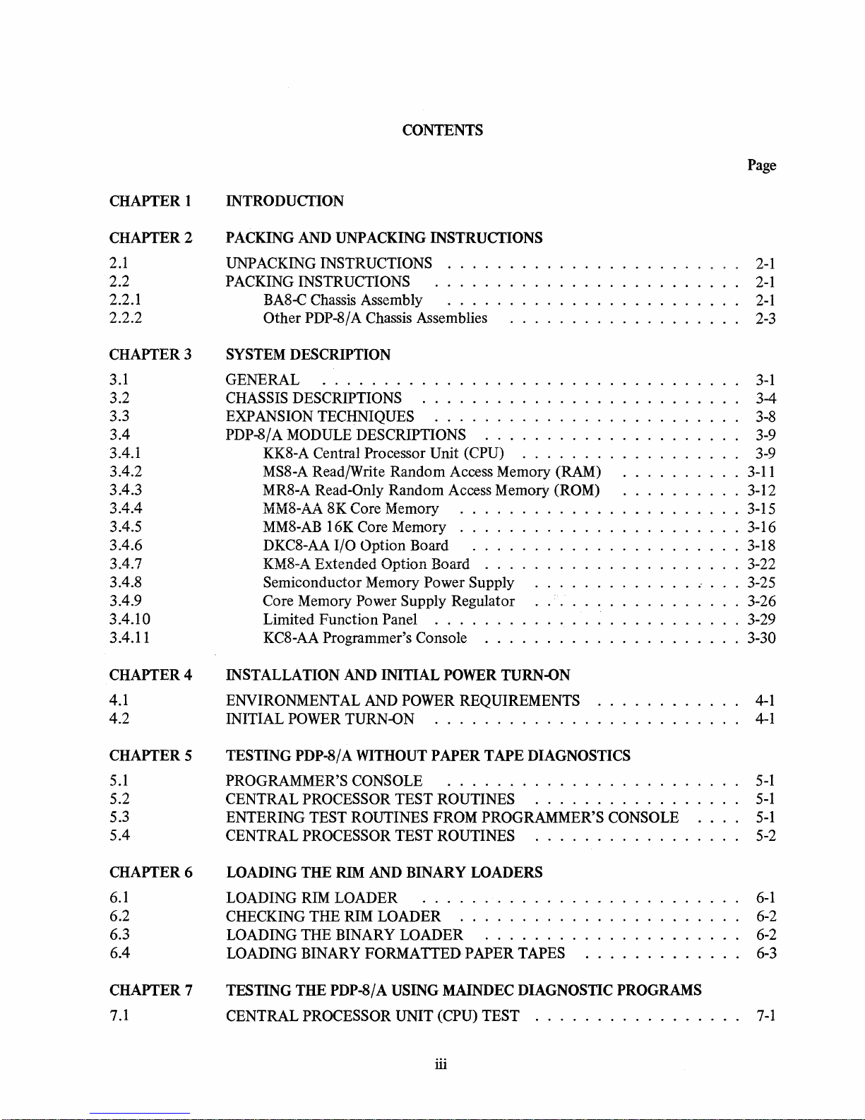
CONTENTS
Page
CHAPTER 1
CHAPTER
2.1
2.2
2.2.1
2.2.2
CHAPTER 3
3.1
3.2
2
3.3
3.4
3.4.1
3.4.2
3.4.3
3.4.5
3.4.6
3.4.7
3.4.8
3.4.9
3.4.10
3.4.11
INTRODUCfION
PACKING AND UNPACKING INSTRUCTIONS
UNPACKING INSTRUCTIONS
PACKING INSTRUCTIONS
BA8-C Chassis Assembly
Other
PDP-8/A Chassis Assemblies
SYSTEM DESCRIPTION
GENERAL
CHASSIS DESCRIPTIONS . . . . . . . . . . . . . . . . . . . .
EXPANSION TECHNIQUES . . . . . . . . . . . . . . . . . . . .
PDP-8/ A MODULE DESCRIPTIONS
KK8-A Central
MS8-A Read/Write Random Access Memory
MR8-A
NHvI8-AA
MM8-AB 16K Core Memory . . . . . . . .
DKC8-AA
K~M8=A
Semiconductor Memory
Core Memory
Limited Function
KC8-AA
.......
Processor Unit (CPU)
Read-Only Random Access Memory (ROM)
8K Core Memory . . . . . . . . . . . . . . 3-15
I/O Option Board
Extended Option Board
Power Supply Regulator
Panel
Programmer's Console
.....
. . . . . . . . . . . . . . . . . . . .
.....................
..................
(RAM)
.......
....
Power Supply . . . . . . . . . . 3-25
...................
........
...
..........
..........
......
.
....
. . . . .
...........
. . . . . . . . . . . 3-30
....
.
....
..
..
..
2-1
2-1
2-1
2-3
3-1
3-4
3-8
3-9
3-9
3-11
3-12
3-16
3-18
3-22
3-26
3-29
CHAPTER
4.1
4.2
CHAPTERS
5.1
5.2
4
5.3
5.4
CHAPTER
6.1
6.2
6
6.3
6.4
CHAPTER
7.1
7
INSTALLATION AND INITIAL POWER TURN-ON
ENVIRONMENTAL AND
INITIAL POWER TURN-ON
TESTING PDP-8/A WITHOUT PAPER TAPE DIAGNOSTICS
PROGRAMMER'S CONSOLE
CENTRAL PROCESSOR TEST ROUTINES
ENTERING TEST ROUTINES FROM PROGRAMMER'S CONSOLE
CENTRAL PROCESSOR TEST ROUTINES . . . . . . . . . . . .
LOADING THE RIM AND BINARY
LOADING
CHECKING THE RIM
LOADING THE BINARY LOADER
LOADING BINARY
TESTING THE PDP-8/A USING MAINDEC DIAGNOSTIC PROGRAMS
CENTRAL PROCESSOR UNIT (CPU) TEST
RIM LOADER
POWER REQUIREMENTS
............
........................
LOADERS
..........
LOADER
FORMATIEDPAPER
.......
.....
iii
.................
.
.
.
TAPES
.
....
. . . . . .
..
..
..
4-1
4-1
5-1
5-1
5-1
5-2
6-1
6-2
6-2
6-3
7-1
Page 5
CHAPTER 8
S.l
S.2
S.3
S.4
CONTENTS (Cont)
ADDITIONAL DIAGNOSTIC TESTS
MEMORY TEST
.........
.
DKCS-AA TEST . . . . . . . . . . .
KMS-A
EXTENDED OPTION BOARD TEST
TESTING
EXTENDED MEMORIES
CHAPTER 9 BASIC PDP-8/A MAINTENANCE
APPENDIX A INSTRUCTION SUMMARY
APPENDIX
B DOCUMENTATION
APPENDIX
C WARRANTY AND MAINTENANCE SERVICES
APPENDIX
D
OMNmus
LOADING
APPENDIX
E POWER CONNECTION
Figure No.
2-1
2-2
2-3
3-1
3-2
3-3
3-4
3-5
3-6
3-7
3-S
3-9
3-10
3-11
3-12
3-13
3-14
3-15
3-16
3-17
3-1S
ILLUSTRATIONS
Title
SA420, SA620, SAS20 Packaging .
PDP-S/A Computer Packaging (Inner)
PDP-S/A Computer Packaging (Outer)
PDP-8/A
Computer
........
.
Part
of
MS320 Module Showing R55, Which is Removed for SA Operation
PDP-8/A Semiconductor
Chassis
..........
.
PDP-8/A Semiconductor Computer Chassis Dimensions
SA Chassis - H9300 (Transformer Cover Removed)
SA620 Chassis . . . . . . . . . . . . . .
SA420/SA620/SAS20 Chassis Dimensions
SA600/SA620 Expansion
.......
.
KKS-A (MS315) CPU Module
.....
.
MSS-A (MS311) Read/Write Random Access Memory
MRS-A (MS312) Read Only Memory (ROM)
MMS-AA SK
Core Memory
.....
MMS-AB
16K Core Memory . . . .
'.
. . . .
DKC8-AA
(MS316) I/O Option Board
D
Etch
Revision
of
DKCS-AA
(MS3l6)
I/O Option Board
KMS-A (MS317) Extended Option Board
.....
Semiconductor Memory Regulator Board (GS016)
SA Master/Slave Switch
.............
.
iv
Page
S-l
S-2
S-6
S-9
Page
2-2
2-4
2-5
3-1
3-3
3-4
3-5
3-6
3-7
3-S
3-9
· 3-10
·
3-11
· 3-13
· 3-15
3-17
·
3-18
· 3-19
..
3-20
3-25
· 3-27
Page 6
Figure No.
3-19
3-20
3-21
6-1
6-2
E-l
Table No.
3-1
3-2
3-3
3-4
3-5
3-6
3-7
3-8
3-9
3-10
3-11
3-12
3-13
3-14
8-1
8-2
9-1
ILLUSTRA
nONS
(Cont)
Title
Core Memory Regulator Board
(G8018)
Limited Function Panel
.....
KC8-AA Programmer's Console
Paper Tape Leader
.......
.
LT33 Teletype Controls
.....
.
PDP-8/ A Electrical Connection
TABLES
Title
PDP-8/ A Computer Assemblies . . . . . . . . . .
PDP-8/ A Computers, Dedicated
Omnibus Slots
....
KK8-A (M8315) Central Processor Unit Switch Settings
MS8-A Read/Write Memory Switch Settings
MR8-A Read
Only Memory Switch
SettLl1gs
. . .
MM8-AA 8K Core Memory Jumper Installation
..
. . . . .
MM8-AB
16K Core Memory Jumper Installation
DKC8-AA
I/O
Option Board Switch Settings, C-Etch Module
DKC8-AA
Option Board Switch Settings, D-Etch Module . .
Auto-Restart Select Switch Settings
..
. . . . . . . . . . .
Bootstrap Select Switch Settings for ROMs Labeled 87 A2 and 88A2
Page
· 3-28
· 3-29
· 3-30
6-2
6-3
E-l
Page
3-2
3-3
· 3-10
..
3-12
·
..
3-14
.....
3-16
·
..
3-16
· 3-20
.....
3-21
..
3-23
· 3-23
· 3-23
·
..
3-24
Bootstrap Select Switch Settings for ROMs Labeled 158A2 and 159 A2
Bootstrap Select Switch Settings for ROMs Labeled 156A2 and 157 A2
Bootstrap/Auto-Restart Switch Settings . . . . . . . . . . . .
.....
Bootstrap Switch Settings for ROMs Labeled
87
A2 and 88A2 (E82 and E87)
Bootstrap Switch Settings for ROMs (E82 and E87) Labeled 158A2 and 159A2
3-24
8-8
8-8
9-1
Basic PDP-8/ A Troubleshooting
.......................
.
v
Page 7

Page 8
CHAPTER 1
INTRODUCTION
There are two basic types
of
computers in the PDP-8/ A family. The first type
is
the
PDP-8/
A, which uses
semiconductor memories (MS8 and MR8). The second type
is
represented by a series
of
computers, each
of
which uses 8K or
16K
core memory (MM8); this series consists
of
the 8A400, 8A420, 8A600, 8A620, 8A800, and
8A820 computers. When a reference applies to both types
of
computers, the designation
"PDP-8/
A"
is
used.
"PDP-8/A
semiconductor" refers to the semiconductor memory computer, while "8A400," for example, refers
to a specific core memory machine and
"8A"
refers to the core memory machines in general.
The
PDP-8fA
Operator's Handbook includes instructions for packing, unpacking, and installing a PDP-8/A
miniprocessor. All computers and modules are tested thoroughly at DIGITAL's manufacturing facilities before
they are shipped. However, many switches and jumper wires can be arranged
by
the customer for specific pur-
poses; furthermore, there
is
a need both to verify system interconnections and site preparations, and to detect
possible hidden damage incurred during shipping. Consequently, a number
of
initial operating tests are also
included in this handbook.
A
PD
P-8
/ A basic system can comprise a variety
of
components. The following three basic systems are the most
common:
1.
A basic PDP-8/ A, * a memory, and a Limited Function Panel. (This computer does not include a KM8
Extended Memory
Option module and, hence, must be a PDP-8/ A semiconductor.)
2.
A basic PDP-8/ A, a memory, a Limited Function Panel, a KM8 Extended Memory Option module,
a DKC8-AA
I/O
Option module, and a Programmer's Console. (Chapter 5 describes operating tests
for this arrangement.)
3.
A basic system as described in
2,
but accompanied by a teletypewriter and diagnostic** programs.
(Chapter 7 describes operating tests for this arrangement.)
*A
basic PDP-8fA
is
defmed as a Central Processor Unit (CPU) and a chassis assembly (chassis, Omnibus, and power supply).
**Diagnostics are test programs written
to
fmd faults
in
the logic. The PDP-8fA programs are supplied
on
paper tape. Diagnostic pro-
grams are optional and may be ordered from
the
Software Distnoution Center, 146 Main St., Maynard,
MA,
01754.
1-1
Page 9

Page 10
2.1
UNPACKING
INSTRUCfIONS
CHAPTER 2
PACKING AND UNPACKING
INSTRUCTIONS
All PDP-8
fA
computers are packaged in two containers; the inner container holds the computer and some kind
of
protective material.
The
steps
in
this section
are
sufficiently general
to
apply to any PDP-8f A.
To
unpack the PDP-8f A computer, proceed as follows.
i.
Open the outer carton and remove the inner carton.
2.
Open the inner carton.
3.
Carefully remove the cardboard from the top and sides
of
the computer.
4.
Carefully remove the computer from the box.
5.
Inspect the computer for damage.
If
the computer
is
damaged, notify the carrier immediately.
6.
Unpack any other boxes included in the shipment.
7.
Check that all equipment, software, manuals, etc., are present as specified on the shipping list inside
the carton.
8.
Save the cartons
and
packing material
to
use if the PDP-8f A is later repacked.
9.
Refer
to
Chapter 4 for PDP-8f A installation procedures.
2.2 PACKING INSTRUCTIONS
Two types
of
packages are used for the PDP-8f A computers. The type used and the applicable packing instruc-
tions depend on the type
of
PDP-8f A chassis assembly.
2.2.1 BA8-C Chassis Assembly
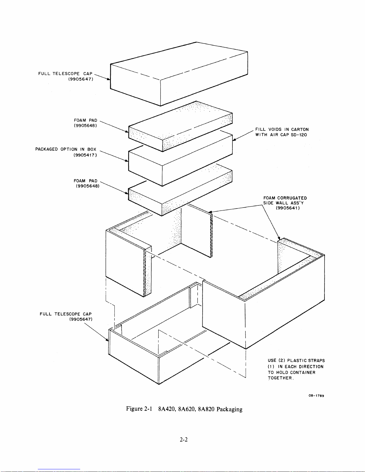
The 8A420, 8A620, and 8A820 computers use a BA8-C chassis assembly (20-slot Omnibus). Figure
2-1
illustrates
the packing procedure. The computer
is
first placed in the inner container (9905417), the empty space
is
filled
with plastic protective material
(AIR
CAP, SD-120), and the container
is
sealed.
The
sealed inner container
is
surrounded with protective foam material which
is
then enclosed by the two telescope caps. Finally, the package
is
secured by two plastic straps.
2-1
Page 11
FULL
TELESCOPE
CAP
(9905647)
FOAM
PAD
(9905648)
PACKAGED
OPTION
IN BOX
(9905417)
FULL
TELESCOPE CAP
(9905647)
Figure
2-1
8A420, 8A620, 8A820 Packaging
2-2
FILL
VOIDS I N CARTON
WITH
AIR
CAP
SD-120
FOAM CORRUGATED
SIDE
WALL
ASS'Y
(9905641
)
ust:
(2)
PLASTIC
STRAPS
(1)
IN
EACH
DIRECTION
TO HOLD CONTAINER
TOGETHER.
08-1789
Page 12

2.2.2 Other
PDP-8/
A Chassis Assemblies
CAUTION
The G8016 Regulator Board assembly used on
PDP-8/A
semiconductor computers contains a battery. This battery,
while not
of
sufficient t'oltage to cause electrical shock,
represents a possible hazard
if
shorted.
If
repacking this
type computer, ensure that there is
no
loose metal, such as
solder, wire, or sheet metal parts, inside the cabinet.
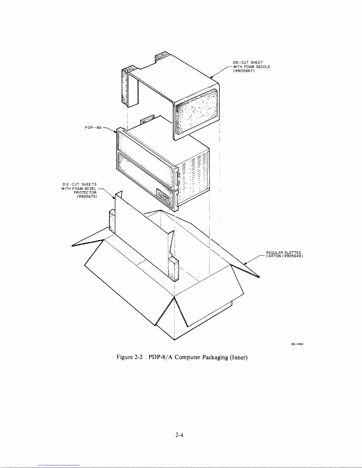
The PDP-8f A semiconductor computer and the 8A400, 8A600,
and
8A800 computers use a chassis assembly
that
has a
lO-s10t
or
12-s10t
Omnibus.
To
pack these computers, proceed as follows.
1.
Place the computer in the smaller
of
the two shipping cartons with the back (side with power cord)
of
the computer against the side
of
the carton.
2.
Place the beveled die-cut sheet with foam protector (part number
9905675)
in front
of
the computer
(Figure 2-2).
If
the Limited Function Panel
and
a pop panel are
on
the computer, the beveled edge
should be down inside the carton.
If
the computer has a Programmer's Console, the beveled edge
should be up
so
that
the cut-out in the cardboard fits the Programmer's Console.
3.
Place the die-cut sheet with foam saddle (part number
9905677)
downward over
the
computer.
The
end with two pieces
of
foam should be fitted around the fans and the other end should be positioned
so that the cardboard fits behind the cabinet mounting flange and the foam
is
against the side
of
the
carton.
4.
Close the flaps and seal the carton with tape.
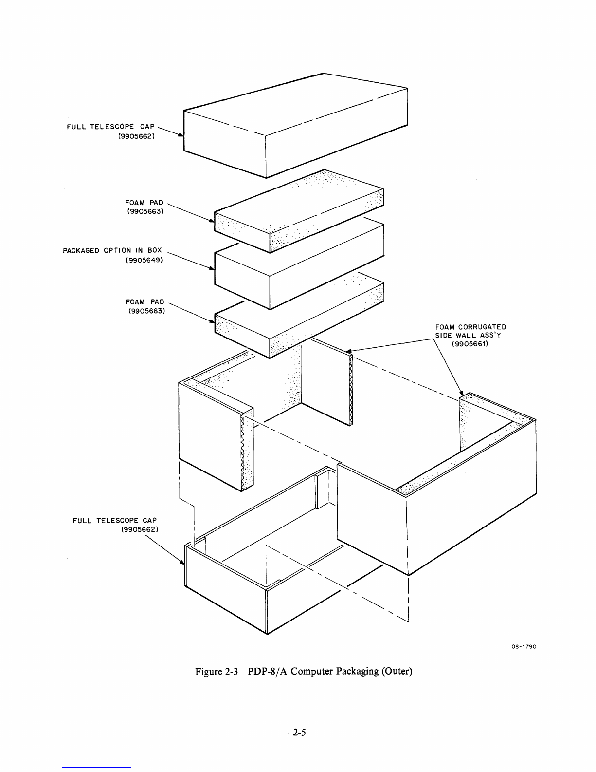
5.
Surround the sealed carton with protective foam material and enclose with telescope caps (Figure
2-
3).
6.
Strap in both directions using steel
or
plastic strapping.
2-3
Page 13
DIE
-CUT
WITH FOAM BEZEL
SHEETS
PROTECTOR
(9905675J
DIE-CUT SHEET
WITH
FOAM
(9905667]
SADDLE
Figure 2-2 PDP-8f A Computer Packaging (Inner)
REGULAR SLOTTED
CARTON
(9905649)
08-1494
2-4
Page 14
FULL
TELESCOPE
CAP
(9905662)
FOAM
PAD
(9905663)
PACKAGED
OPTION
IN BOX
(9905649)
FOAM
PAD
(9905663)
FOAM CORRUGATED
SIDE
WALL
ASS'Y
~
(9905661)
~
Figure
2-3
PDP-8f A Computer Packaging (Outer)
,
2-5
08-1790
Page 15

Page 16
CHAPTER 3
SYSTEM DESCRIPTION
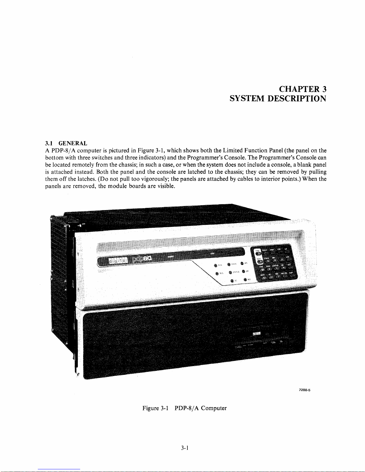
3.1
GENERAL
A
PDP-8/
bottom with three switches and three indicators) and the Programmer's Console. The Programmer's Console can
be located remotely from the chassis; in such a case,
is
attached instead. Both the panel
them
panels
A computer
off
the latches.
are
removed, the module boards
is
pictured in Figure 3-1, which shows
(Do
not
both
the Limited Function Panel (the panel on the
or
when the system does not include a console, a blank panel
and
the console are latched to the chassis; they can be removed by pulling
pull too vigorously; the panels are attached by cables to interior points.) When the
are
visible.
Figure
3-1
PDP-8/A
3-1
7288-5
Computer
Page 17
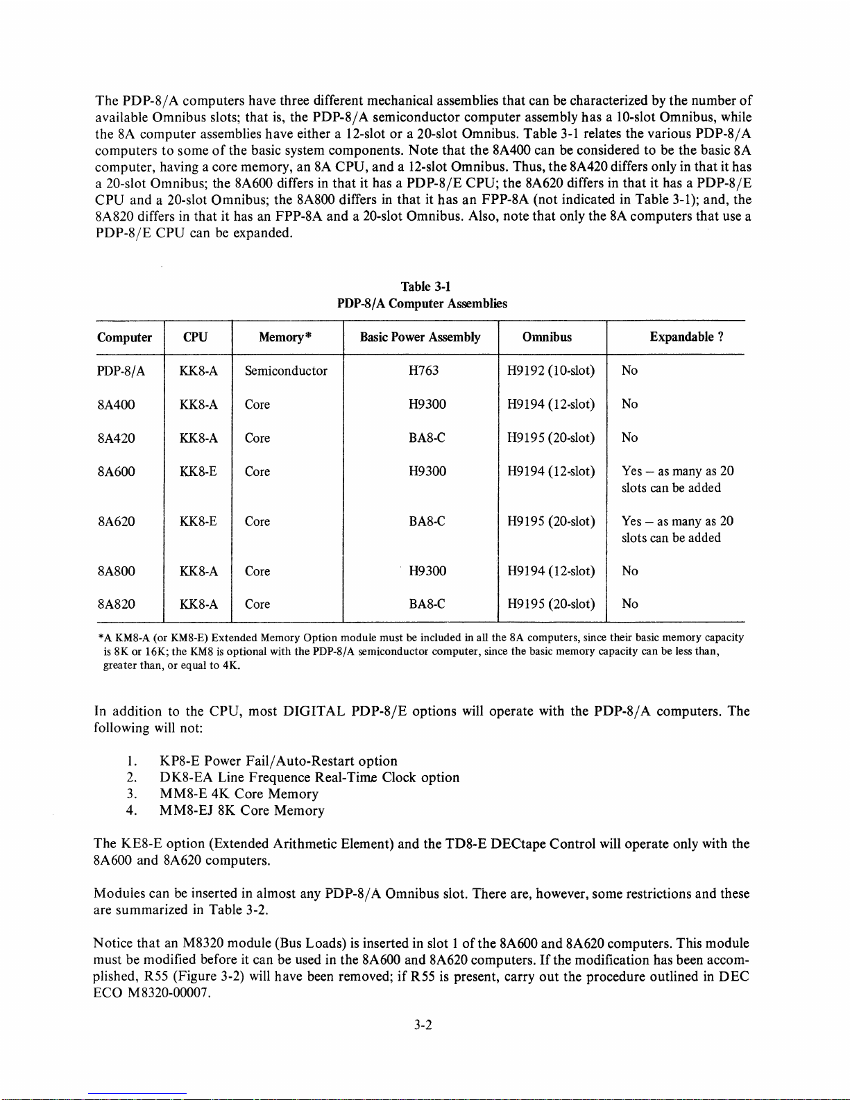
The
PDP-SI
A computers have three different mechanical assemblies
that
can be characterized by
the
number
of
available Omnibus slots;
that
is, the
PDP-SI
A semiconductor
computer
assembly
has
a IO-slot Omnibus, while
the
SA
computer assemblies have either a 12-slot
or
a 20-slot Omnibus. Table
3-1
relates the various PDP-S I A
computers
to
some
of
the basic system components.
Note
that
the
SA400 can be considered to be the basic SA
computer,
having a core memory,
an
SA
CPU,
and
a 12-slot Omnibus. Thus,
the
SA420 differs only in
that
it has
a
20-slot Omnibus; the SA600 differs in
that
it has a
PDP-S/E
CPU;
the
SA620 differs in
that
it has a
PDP-S/E
CPU
and
a 20-s10t Omnibus; the
SASOO
differs
in
that
it
has
an
FPP-SA
(not
indicated in Table 3-1);
and,
the
SAS20 differs in
that
it has an FPP-SA
and
a 20-s10t Omnibus. Also, note
that
only the
SA
computers
that
use a
PDP-S/E
CPU
can be expanded.
Table
3-1
PDP-8fA Computer Assemblies
Computer
CPU
Memory *
Basic Power Assembly
Omnibus
Expandable ?
PDP-8fA
KK8-A
Semiconductor
H763 H9192
(1
O-sIot)
No
8A400
KK8-A
Core
H9300
H9194 (12-s10t)
No
8A420
KK8-A
Core
BA8-C
H9195 (20-slot)
No
8A600
KK8-E
Core
H9300 H9194 (12-slot)
Yes -as
many
as
20
slots can
be
added
8A620
KK8-E
Core
BA8-C
H9195 (20-slot)
Yes -as
many
as
20
slots can
be
added
8A800
KK8-A
Core
H9300
H9194 (12-slot)
No
8A820
KK8-A
Core
BA8-C
H9195 (20-slot)
No
* A
KMS-A
(or
KMS-E)
Extended Memory Option module must
be
included
in
all the
SA
computers, since their basic memory capacity
is
SK
or 16K; the
KMS
is
optional with the PDP-Sf A semiconductor computer, since the basic memory capacity can be less than,
greater than, or equal to 4K.
In addition to the
CPU,
most
DIGITAL
PDP-S/E
options
will
operate
with the
PDP-S/A
computers. The
following will not:
1.
KPS-E Power
Faill
Auto-Restart
option
2.
DKS-EA Line Frequence Real-Time Clock
option
3.
MMS-E
4K
Core
Memory
4. MMS-EJ SK
Core
Memory
The
KES-E
option
(Extended Arithmetic Element)
and
the
TDS-E
DECtape
Control
will
operate
only with the
SA600 and SA620 computers.
Moduies
can
be inserted in almost any
PDP-SI
A Omnibus slot. There are, however, some restrictions
and
these
are summarized in Table 3-2.
Notice
that
an MS320 module (Bus Loads)
is
inserted in slot 1
of
the
SA600
and
SA620 computers. This module
must be modified before it can be used in the
SA600 and SA620 computers.
If
the modification has been accom-
plished, R55 (Figure 3-2) will have been removed;
if
R55 is present, carry
out
the procedure outlined in
DEC
ECO
MS320-00007.
3-2
Page 18
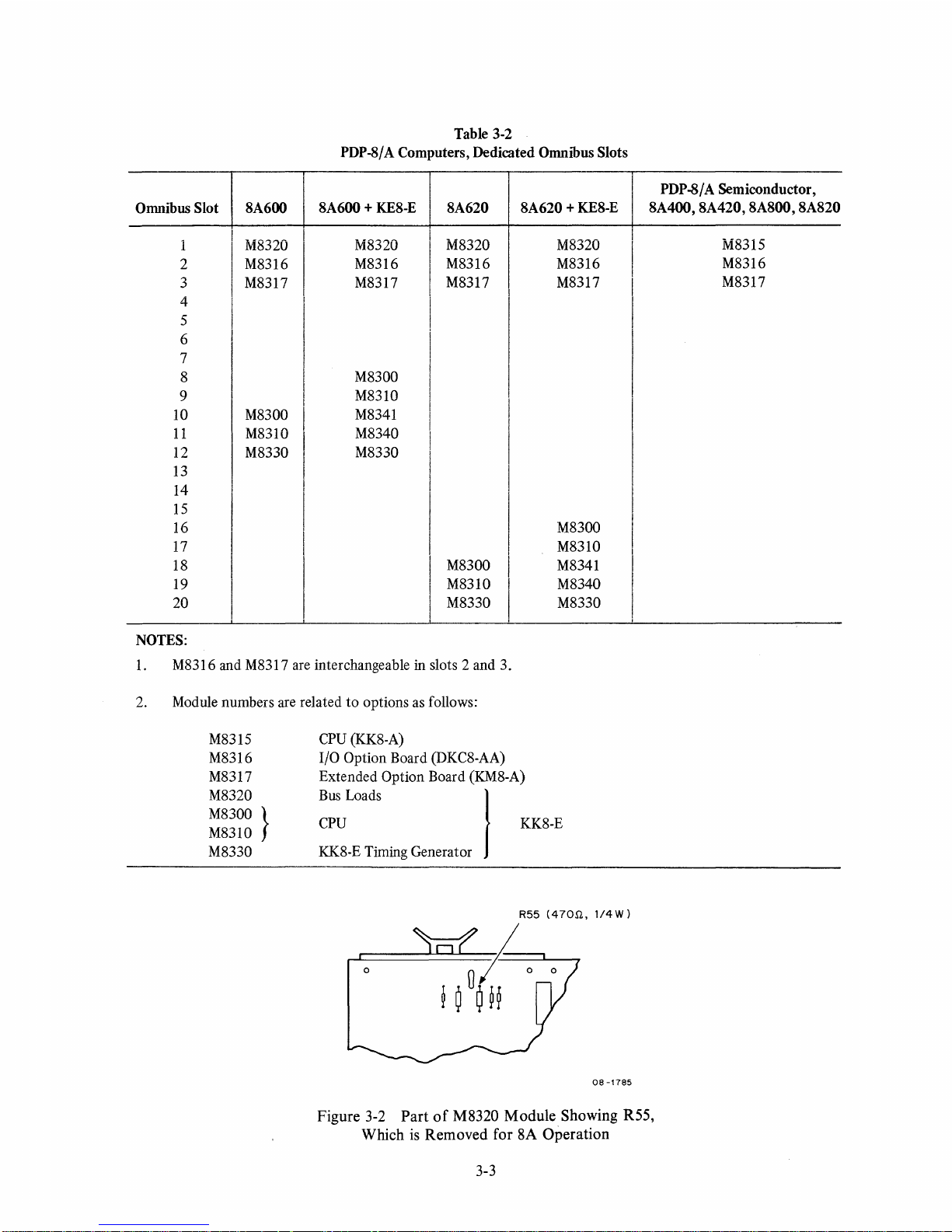
Table 3-2
PDP-Sf A Computers, Dedicated Omnibus Slots
PDP-8/ A Semiconductor,
Omnibus Slot SA600 SA600 + KES-E SA620
SA620
+ KES-E
SA400, SA420,
SASOO,
SAS20
1
2
3
4
5
6
7
8
9
10
11
12
13
14
15
16
17
IS
19
20
NOTES:
I
M8320
M8316
M8317
I
I
I
M8300
I
M8310
M8330
M8320
I
M8316
M8317
I
M8300
M8310
M8341
M8340
I
M8330
I
M8320
M8316
M8317
MS300
MS310
MS330
M8320
M8316
M8317
MS300
MS310
MS341
MS340
MS330
I
I
I
I
1. MS316 and MS317 are interchangeable in slots 2 and 3.
2. Module numbers are related
to
options as follows:
MS315
MS316
MS317
MS320
MS300 }
MS310
MS330
CPU
(KKS-A)
I/O Option Board (DKCS-AA)
Extended Option Board (KMS-A)
Bus Loads
I
CPU
KKS-E
Timing Generator
KKS-E
08
-1785
Figure
3-2
Part
of
M8320 Module Showing R55,
Which
is
Removed for 8A Operation
3-3
M8315
M8316
M8317
Page 19

3.2 CHASSIS DESCRIPTIONS
Three chassis types are available. The
PDP-8/
A semiconductor computer chassis
is
illustrated in Figure 3-3. (The
front panels have been removed.) Modules are inserted in the Omnibus from the front
of
the unit. Both quad-and
hex-size modules can be inserted;
the
fingers
on
connectors E
and F of
the hex size modules do
not
carry
Omnibus signals. (Some hex modules
do
not
have connectors E
and
F.) Figure 3-4 illustrates the dimensions
of
the same computer, as well as indicating the ac line
and
fuse locations.
G8016
REGULATOR
ASSEMBLY
POWER
CONTROL
FUSE
MASTER-SLAVE
SWITCH
Figure 3-3 PDP-8 / A Semiconductor Chassis
3-4
LIMITED
FUNCTION
PANEL
7.2884
Page 20
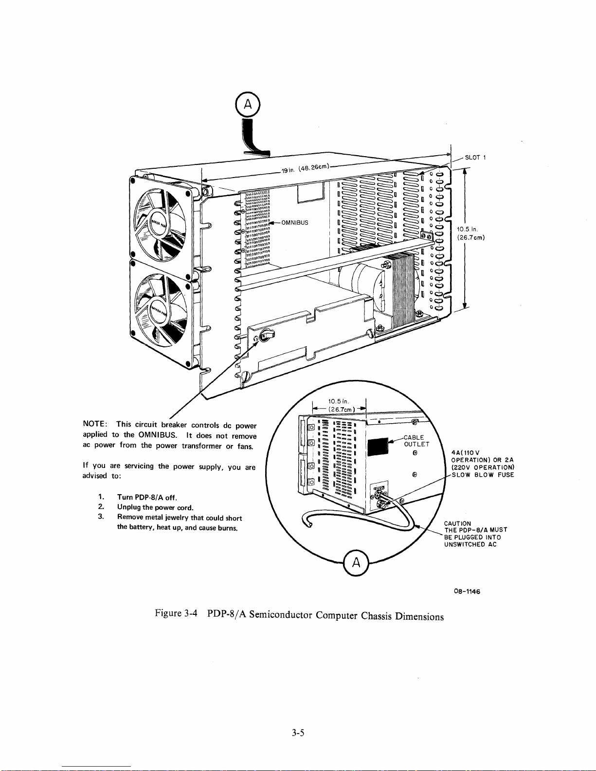
'\9
in.
l48.
26cm)
NOTE:
applied
ac
power
If
you
advised
1.
2.
3.
This
circuit
to
the
OMNIBUS.
from
the
are servicing
breaker
power
the
controls
It
does
transformer
power
supply,
not
to:
Turn PDP-8/A
off.
Unplug the power cord.
Remove metal jewelry that could short
the battery, heat up, and
cause
burns.
Figure 3-4 PDP-8f A Semiconductor Computer Chassis Dimensions
dc power
remove
or
fans.
you
are
4A(110V
OPERATION)
(220V
OPERATION)
SLOW
BLOW
08-1146
OR
FUSE
2A
3-5
Page 21
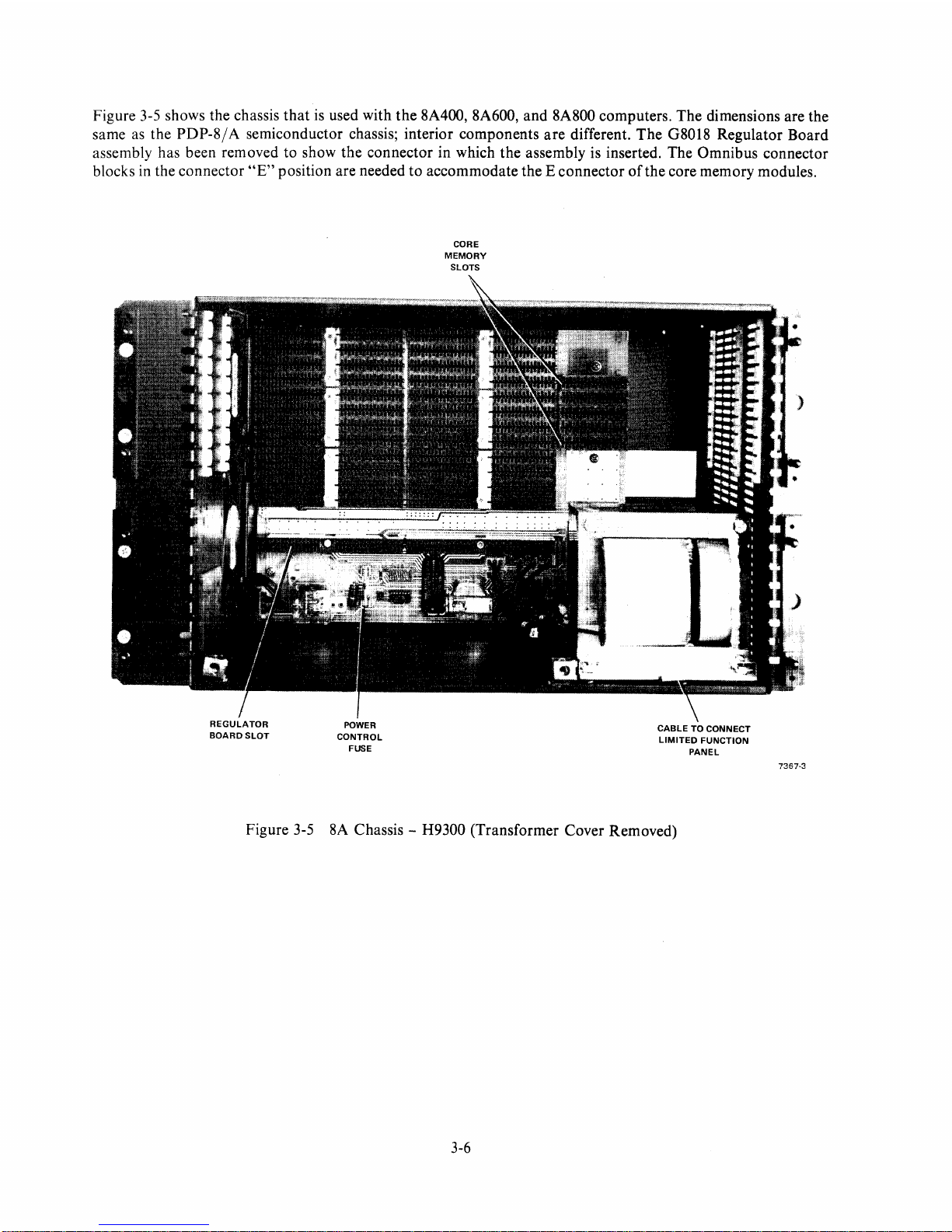
Figure 3-5 shows the chassis
that
is
used with
the
8A400, 8A600, and 8A800 computers. The dimensions are the
same as the
PDP-8/
A semiconductor chassis; interior components
are
different.
The
08018
Regulator Board
assembly has been removed to show the connector in which
the
assembly is inserted. The Omnibus connector
blocks in the connector
HE" position are needed
to
accommodate the E connector
of
the core memory modules.
REGULATOR
BOARD
SLOT
POWER
CONTROL
FUSE
CORE
MEMORY
SLOTS
CABLE
TO CONNECT
LIMITED
FUNCTION
PANEl
Figure 3-5 8A Chassis - H9300 (Transformer Cover Removed)
3-6
7367-3
Page 22
Figure
3-6
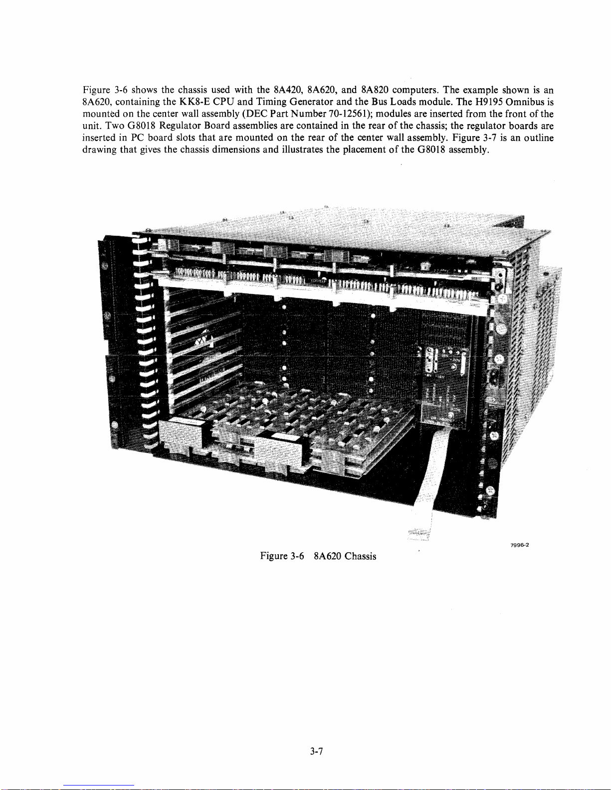
shows the chassis used with the 8A420, 8A620, and 8A820 computers. The example shown
is
an
8A620, containing the KK8-E
CPU
and Timing Generator
and
the Bus Loads module. The H9195 Omnibus
is
mounted on the center wall assembly (DEC
Part
Number
70-12561); modules are inserted from the front
of
the
unit. Two G8018 Regulator Board assemblies are contained in the rear
of
the chassis; the regulator boards are
inserted in
PC board slots
that
are mounted on the rear
of
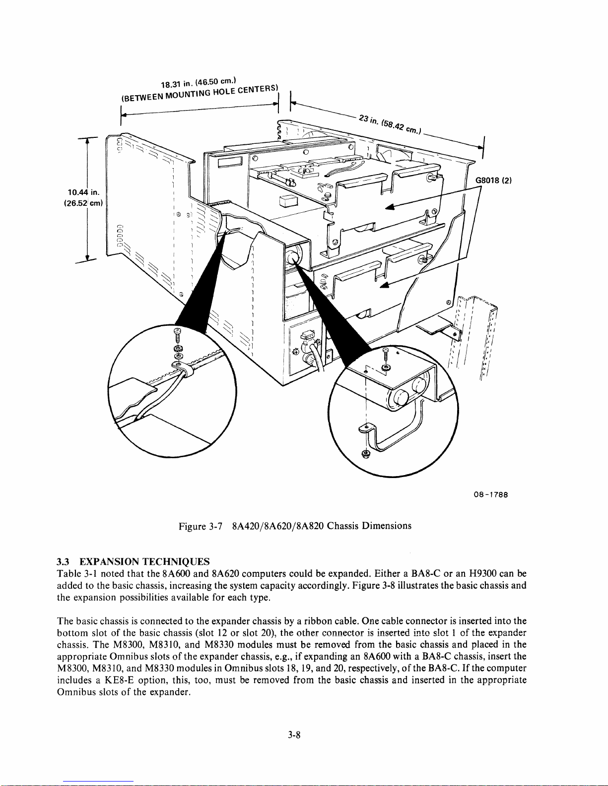
the center wall assembly. Figure 3-7
is
an outline
drawing that gives the chassis dimensions
and
illustrates the placement
of
the G8018 assembly.
7996-2
Figure 3-6 8A620 Chassis
3-7
Page 23
(BElWEEN
1831
in.
(46.50 em.)
~OUNTING
HOLE
CENTER~
~
T
10.44
in.
(26.52: em)
1
~
~~~
8.42
e,".)
~
Figure 3-7 SA420 /SA620 /SAS20 Chassis Dimensions
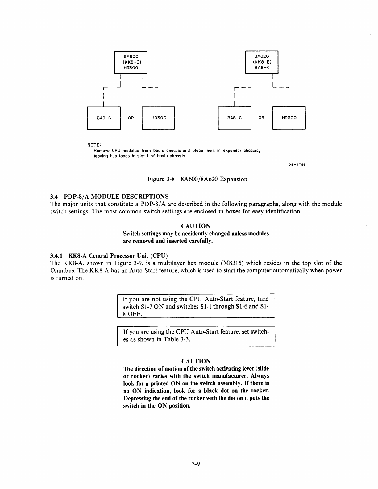
3.3 EXPANSION TECHNIQUES
Table
3-1
noted
that
the SA600
added to the basic chassis, increasing the system capacity accordingly. Figure
the expansion possibilities available for each type.
The basic chassis
bottom
chassis. The
appropriate
MS300, MS310, and MS330 modules in Omnibus slots IS,
includes a
Omnibus slots
slot
is
connected to the expander chassis by a ribbon cable.
of
the basic chassis (slot
MS300, MS310, and MS330 modules must
Omnibus slots
KES-E option, this, too, must be removed from the basic chassis
of
the expander.
and
of
the
expander chassis, e.g.,
SA620 computers could be expanded. Either a BAS-C
3-S
illustrates the basic chassis and
One
cable connector
12
or
slot 20), the
other
connector
be
removed from the basic chassis
if
expanding an SA600 with a BAS-C chassis, insert the
19,
and 20, respectively,
3-S
is
inserted into slot 1
of
the BAS-C.
and
inserted in the appropriate
08
-1788
or
an H9300 can be
is
inserted into the
of
the expander
and
placed in the
If
the computer
Page 24
SA600
(KKS-E)
H9300
I
L_-,
I
BORB
NOTE:
SA620
(KKS-E)
BAS-C
Remove
CPU
modules from basic chassis and place them in expander chassis,
leaving bus loads in
slot 1 of
basic chassis.
Figure 3-8 8A600 /8A620 Expansion
3.4
PDP-8f
A
MODULE
DESCRIPTIONS
08
-1786
The major units
that
constitute a
PDP-8/
A are described in
the
following paragraphs, along with
the
module
switch settings. The most common switch settings
are
enclosed in boxes for easy identification.
CAUTION
Switch settings may be accidently changed unless modules
are removed and inserted carefully.
3.4.1
KKS-A Central Processor Unit
(CPU)
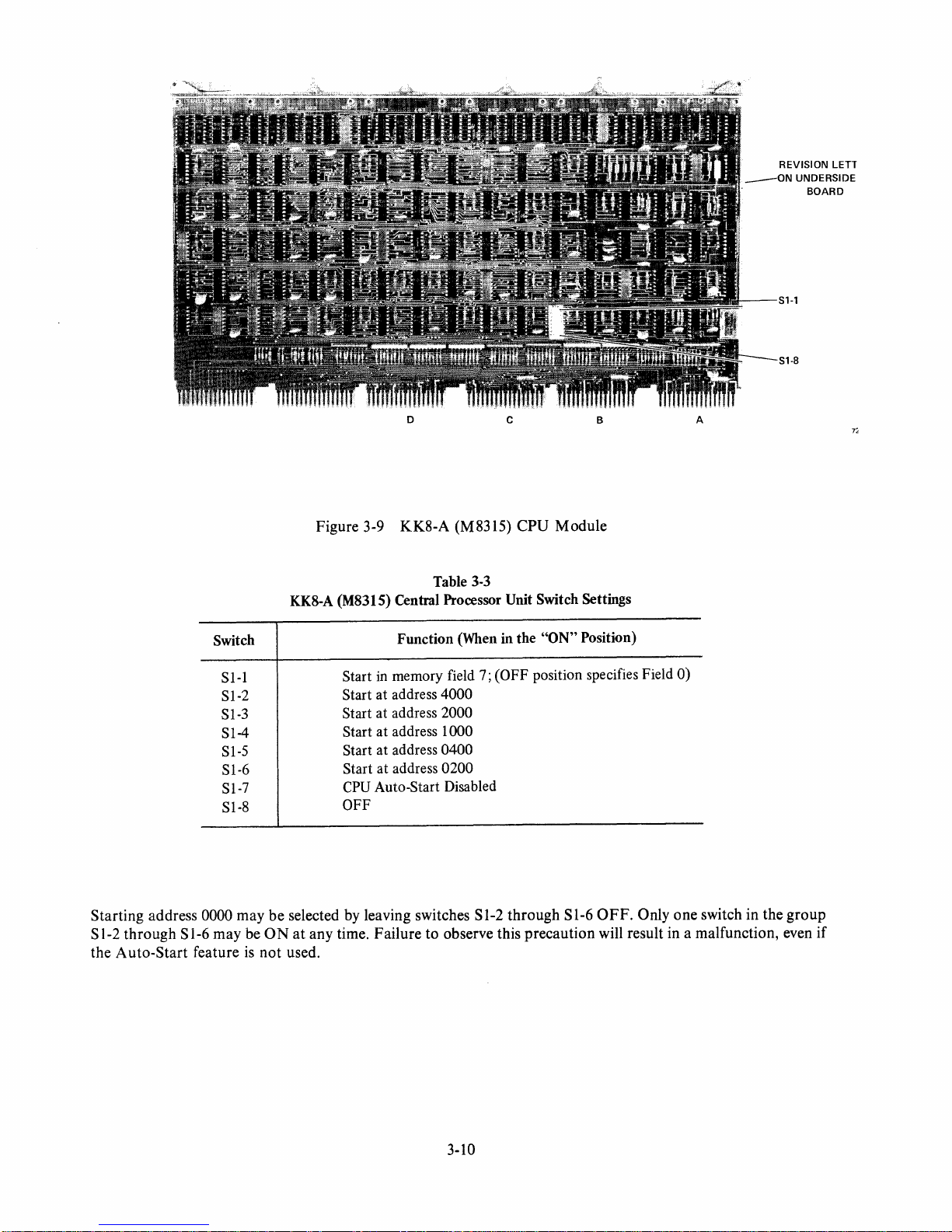
The KK8-A, shown in Figure 3-9,
is
a multilayer hex module (M8315) which resides in the
top
slot
of
the
Omnibus. The KK8-A has an Auto-Start feature, which
is
used to start
the
computer automatically when power
is
turned on.
If
you
are
not
using the
CPU
Auto-Start feature,
turn
switch SI-7
ON
and
switches SI-1
through
S1-6
and
SI-
8
OFF.
If
you are using
the
CPU
Auto-Start feature, set switch-
es
as shown in Table 3-3.
CAUTION
The direction
of
motion
of
the switch activating lever (slide
or rocker) varies with the switch manufacturer. Always
look for a printed
ON
on
the switch assembly.
If
there is
no
ON indication, look for a black dot on the rocker.
Depressing the end
of
the rocker with the dot on it puts the
switch in the
0 N position.
3-9
Page 25
__
ON
REVISION LETT
UNDERSIDE
BOARD
S1-1
S1-8
Switch
Sl-l
SI-2
SI-3
Sl4
Sl-S
SI-6
Sl-7
SI-8
D
Figure
KK8-A (M8315) Central Processor Unit Switch Settings
Start
3-9
KK8-A
Function
in
memory field 7; (OFF position specifies Field 0)
(M8315)
Table 3-3
(When in
c
CPU
the
Module
"ON"
B
Position)
Start at address 4000
Start at address 2000
Start at address looO
Start at address 0400
Start at address 0200
CPU
Auto-Start Disabled
OFF
A
Starting
SI-2
the
address 0000
through
Auto-Start
Sl-6
feature
may
may
be
is
be
selected by leaving switches
ON
at
any
not
used.
time.
Failure
Sl-2
to
observe this
3-10
through
precaution
Sl-6
OFF.
Only
one
switch
will result in a malfunction, even
in
the
group
if
Page 26
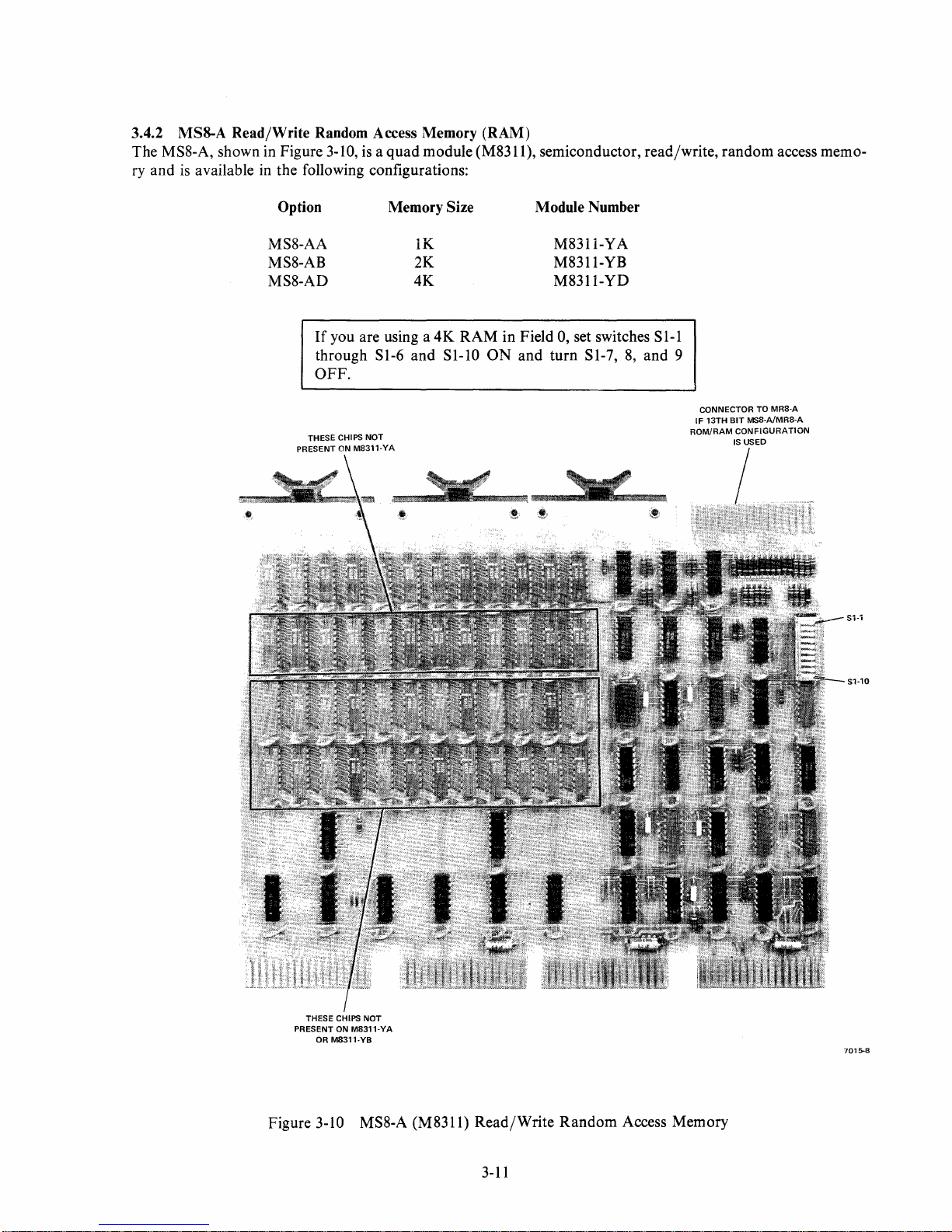
3.4.2 MS8-A
MS8-A, shown in Figure 3-10,
The
ry and
is
Read/Write
available in the following configurations:
Random Access Memory (RAM)
is a quad
module (M8311), semiconductor, read/write,
random
access memo-
Option
MS8-AA
MS8-AB
MS8-AD
If
through SI-6
OFF.
Memory Size
lK
2K
4K
you are using a
and
4K
SI-10
Module Number
M8311-YA
M8311-YB
M8311-YD
RAM
in Field 0, set switches SI-1
ON
and
turn
SI-7,
8,
and 9
CONNECTOR TO MRS-A
IF
13TH
BIT
ROM/RAM
MSS-A/MRS-A
CONFIGURATION
S1-1
THESE CHIPS
PRESENT ON
OR
MS311-YA
M8311-YB
NOT
Figure 3-10 MS8-A (M8311)
Read/Write
Random
S1-10
7015-8
Access Memory
3-11
Page 27
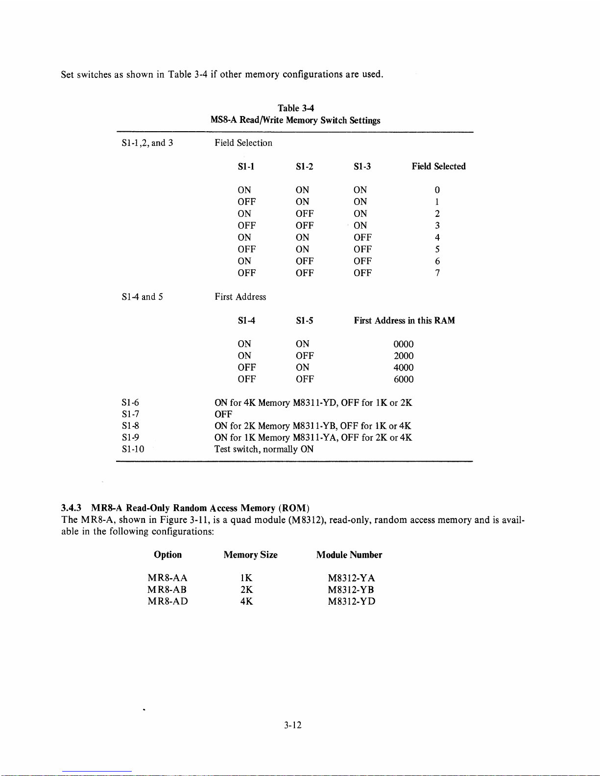
Set switches
as
shown
in
Table
3-4
if
other
memory
configurations
are
used.
Table
34
MS8-A
Read/Write Memory Switch Settings
SI-1 ,2, and 3 Field Selection
SI-1 SI-2
81-3
Field Selected
ON
ON ON
0
OFF ON
ON
1
ON
OFF
ON
2
OFF OFF
ON
3
ON ON
OFF 4
OFF
ON
OFF
5
ON
OFF
OFF
6
OFF
OFF
OFF
7
Sl-4and5
First Address
SI-4 81-5 First Address
in
this
RAM
ON ON
0000
ON OFF
2000
OFF
ON
4000
OFF OFF
6000
SI-6
ON
for
4K
Memory M8311-YD, OFF for 1K or 2K
SI-7
OFF
SI-8
ON
for 2K Memory M8311-YB, OFF for
lK
or
4K
SI-9
ON
for
lK
Memory M8311-YA, OFF for 2K or
4K
Sl-10
Test switch, normally
ON
3.4.3 MRS-A Read-Only Random Access Memory
(ROM)
The
MRS-A,
shown in
Figure
3-11, is a
quad
module
(MS312), read-only,
random
access
memory
and
is avail-
able in
the
following configurations:
Option
MRS-AA
MRS-AB
MRS-AD
Memory Size
lK
2K
4K
3-12
Module Number
MS312-YA
MS312-YB
MS312-YD
Page 28

S9-1
S9-8
THESE
THREE
CONNECTORS
ARE
REMOVED
TO
PROGRAM
THE
ROM,
BUT
THEY
MUST
BE
IN
PLACE
FOR
NORMAL
OPERATION
CONNECTOR
TO
MS8-A
IF
13TH
BIT
MS8-A/MR8-A
ROM/RAM
CONFIGURATION
IS
USED
Figure 3-11
MR8-A
(M8312)
Read
Only
Memory
(ROM)
The
first address
is
always location 0000
of
the
selected memory field.
I f you
are
using a 4K
ROM
in Field 0 with no connections
to
RAM,
set the following switches
ON:
SI-1 through SI-8;
S3-1
through S3-8;
S5-1
through S5-8;
S7-1
through S7-8;
S8-1
through S8-8;
S9-1
through S9-8; S4-1, 2,
3,4,
6, 7;
and
S6-3
through S6-8. Set the following switches OFF:
S2-1
through S2-8; S4-5, 8; S6-1, 2.
If a RAM
is
used with
top connectors, change
S4-7
to
OFF and
S4-8
to
ON.
3-13
S3
S1-1
Sl·8
54
S2
7230-1
Page 29

Set switches
as
shown
in Table 3-5
All switches must be
grammed (i.e., while
if
MRS-
other
configurations
are
used.
CAUTION
OFF
when the M8312 is being pro-
data
is being loaded into
Table 3-5
A Read Only Memory Switch Settings
ROM).
Switch
SI-1 to SI-8
S2-1
,8, and 5
82-2 and 4
82-3,6 and 7
Function/Position
ON
Size 8elect 8witch 8ettings
S2
..
S2-1
ON
ON
OFF
OFF
Field 8elect 8witch 8ettings
Field
0
1
2
3
4
5 ON
6 OFF
7
S
ON
ON
OFF
S2·6
OFF
ON
OFF
ON
OFF
ON
S2-5
OFF
OFF
OFF
S2-3
OFF
OFF
ON
ON
OFF
OFF
ON
ON
Memory Size
lK
2K
4K
S2-7
OFF
OFF
OFF
OFF
ON
ON
ON
ON
S3-1
to
S3-8
84-1,2,3,4, and 6
84-5
84-7
84-8
85-1
to
S5-8
86-1
and 86-2
86-3,4,5,6,7, and 8
87-1
to
87-8
88-1
to
88-8
89-1
to
89-8
ON
ON
OFF
OFF
for ROM/RAM Combination; otherwise
ON
for ROM/RAM Combination; otherwise OFF
ON
OFF
ON
ON
ON
ON
3-14
ON
Page 30

3.4.4 MM8-AA
The
MM8-AA,
of
core memory.
8K
Core Memory
shown in Figure 3-12,
If
you
are using core memory
Wl-3
and
is
a hex module (G649) with
in
Wl-2
and remove W2-4
an
Fields 0
and
W3-4.
H219-A Stack Assembly
and
1,
install
that
contains
8K
Figure 3-12 MMS-AA SK
3-15
Core
7388-2
Memory
Page 31

Install
or
remove
jumpers
as
shown
MM8-AA
in
Table
8K
3-6
if
other
Table
3-6
Core Memory
memory
Jumper
fields
are
Installation
in
use.
3.4.5
The
of
core
I nstall
Fields Used
o and 1
2 and 3 Removed
4 and 5 In Removed
6 and 7 Removed Removed
MMS-AB
MMS-AB,
memory.
or
remove
16K
shown
jumpers
Core
in
Figure
as
WI-3
In
Memory
3-13, is a
If
the
MMS-AB
ers
WI-3
W3-4
should
shown
MM8-AB
and
in
hex
Wl-2
be
Table
16K
module
is
removed.
WI-2 W2-4 W3-4
In
In
(0650)
installed
3-7
Core Memory
should
if
other
Table 3-7
in
be
Removed
In
Removed
In
with
an
H219-B
Fields 0 through
installed
memory
Jumper
and
fields
Installation
Stack
3,
jump-
W2-4
are
used.
Assembly
and
Removed
Removed
In
In
that
contains
16K
Fields Used
o to 3
4
to
7
WI-3 WI-2 W2-4
In
Out
In
In
Out
In
3-16
W3-4
Out
Out
Page 32

7388-1
Figure
3-13
MMS-AB
3-17
16K
Core Memory
Page 33

3.4.6 DKC8-AA
There
14).
the
(side 1
are two
OK
other
as etch revision D (shown in
is
the
component
viewing side 2).
I/O
Option Board
C8-AA
hex
modules
(M 8316) in existence;
side). Lettering
Figure
similar
3-15).
to
the
one
The
etch
following
is defined as
etch
revision C (shown in
revision is identified
appears
near
the
on
side 2
of
lower right
Figure
the
PC
corner
3board
(when
Option
Board
1
Side 2
M8316
50109000
The
letter
0 indicates
the 0 etch
revision level; differences
S1-1
that
exist
revision.
are
indicated in
The
information
the
description.
in
this section is
J1
PROGRAMMERS
CONSOLE
not
totally applicable
J2 PROGRAMMERS
CONSOLE (CONNECTS
TO BOTTOM CONNEC-
TOR OF PROGRAMMERS
CONSOLE)
to
each
J5
PARALLEL
If 0
TRANSMIT
J4
PARALLEL
If 0 RECEIVE
J3
SERIAL
LINE
UNIT
-
{
{ "
------"'!'
..
,',
Figure
3-14
OKC8-AA
(M8316)
I/O
Option
7015-6
Board
3-18
Page 34

REVISION LETTER
ON
UNDERSIDE
OF
BOARD (SIDE 2)
J3
SERIAL
LINE
UNIT
J5
PARALLEL
I/O
TRANSMIT
J4
S1-1
S1-10
PARALLEL
I/O
RECEIVE
SIDE
1
J2
PROGRAMMER'S
CONSOLE (CONNECTS)
TO BOTTOM
CONNECTOR
OF
PROGRAMMER'S CONSOLE
J1
PROGRAMMERS
CONSOLE
Figure 3-15 0 Etch Revision
of
OKC8-AA
(M8316)
I/O
Option
Board
The 0 KC8-AA combines four options:
8071-1
L Serial Line
Unit
(SLU),
110
to
9600 (50
to
9600 for revision
D)
baud
rate interface for Teletype,@
VT50,
or
other
compatible serial line unit
2_
Real-Time Clock - Crystal controlled
at
100
Hz
3_
General-Purpose Parallel
I/O
- 12-bit
I/O
for
user's device
or
another
POP-8/
A
NOTE
The General-Purpose Parallel
I/O
on
the D etch revision
of
the M8316 module can
be
used
as
an interface for the
LA180.
Data
to
the LA180 must be supplied in com-
plemented form. The
lOTs
are
different from the LA8
interface designed for the LAl80. A BC80-A cable, available from DIGITAL, must be used to connect the GeneralPurpose Parallel
I/O
to the LA180.
®Teletype
is
a registered trademark
of
Teletype Corporation.
3-19
Page 35

4.
Console Logic - Logic
to
connect the
KC8-AA
Programmer's
Console
to
the
Omnibus
Revision C:
For
Teletype (ASR33)
operation
without
real-time clock software, set switches S 1-4, 6,
and 8 to
the
ON
position; set switches SI-1, 2,
3,
5,
and 7 to
the
OFF
position.
Revision D:
For
Teletype (ASR33) operation
without
real-time clock software, set switches
SI-I,
3,4,6,8,
and
9
to
the
ON
position; set switches
Sl-2,
5,
and 7 to
the
OFF
position.
(Sl-10
is
a spare.)
For
other
operation, set switches as shown in Tables 3-8 and 3-9.
Table 3-8
DKC8-AA
I/O Option Board Switch Settings, C-Etch Module
Switch
Function
Sl-1,2and3
Baud Rate
as
shown in Table below:
SI-1
SI-2
SI-3 Baud Rate
OFF
OFF
OFF
110
OFF
OFF
ON
150
OFF
ON
OFF
300
OFF
ON ON
600
ON
OFF OFF
1200
ON
OFF
ON
2400
ON
ON
OFF
4800
ON ON
ON
9600
S14
Clear Data Available at Time State 1 (normally
ON)
Sl-5
ON
enables Real Time Clock
Sl-6
Test (normally
ON,
OFF
for special testing)
Sl-7
ON
for 1 stop bit,
OFF
for two stop bits
Sl-8
ON
enables TTY filter
in
20
rnA
CKT
(used only for 100 baud)
3-20
Page 36

Table 3-9
DKC8-AA Option Board Switch Settings, D-Etch Module
Switch
Sl-1, 2, 3, and 4
Sl-5
Function
as
Baud rate
*OFF
ON
= Real Time Clock enabled
OFF = Read Time Clock disabled
shown in table below:
SI-4 SI-3
ON
ON
ON ON
ON
ON
ON
ON
ON
OFF
OFF
OFF ON
OFF
OFF
OFF
OFF
ON
ON
ON
OFF
OFF
OFF OFF
OFF
ON
ON
ON
OFF
OFF
OFF
OFF
SI-2
ON
ON
OFF
OFF
ON
ON
OFF
ON
ON
OFF
OFF OFF 3600
ON
ON
OFF
OFF
SI-1 Baud Rate
ON
OFF
ON
OFF
ON 150
OFF 300
ON 600
OFF 1200
ON
OFF 2000
ON
ON
OFF 7200
ON
OFF 19.2K
50
75
110
134.5
1800
2400
4800
9600
Sl-6
Sl-7
Sl-8
Sl-9
*Serial Line will
ON
= Test Switch (always ON)
ON
= 1 Stop Bit in SLU character
OFF = 2 Stop Bits in SLU character
ON;:: ASR/KSR 33 DR35 fIlter in (across SLU 20 rnA REC'V Leads.
ON
if
Baud Rate
OFF -filter out
ON = TS1
OFF
not
run at this baud rate. This setting
clears DATA AVAIL flip-flop in Parallel I/O Section
= DATA AVAIL
is
110
or
not
is
below.)
cleared by TSI
not
to be used.
3-21
Page 37

3.4.7 KMS-A Extended Option Board
The KMS-A, shown in Figure 3-16,
is
Power-Fail/ Auto-Restart
Bootstrap Loaders - Provide commonly used
and
Memory Extension
Timeshare Control
If
you are using paper tape under control
strap switches, no Auto-Restart, and timeshare enabled,
set the following switches
S2-1, S2-5 through S2-7; set the following switches
Sl-5 through Sl-7, S2-2 through S2-4,
a hex module (MS317)
I/O
loaders
ON:
SI-1 through SI-4, SI-S,
that
combines the following options:
of
the boot-
OFF:
and
S2-S.
Figure 3-16 KMS-A (MS317) Extended
3-22
Option
7299-1
Board
Page 38

Other
switch settings for
the
KM8-A
are listed in Tables 3-10
through
3-14.
Program
S2-5
Hi-Lo
RIM*
ON
RK8-E*
ON
TC08*
ON
RF08/DF32D*
OFF
TA8-E*
OFF
NOTE
There
are
three types
of
bootstrap
ROMs
used on the
KM8-A. E82 and E87 have different labels for the different bootstrap
ROMs.
Switches on modules
that
have E82
and E87 (Figure 3-16) labeled 87A2 and 88A2 should be
set according to Table 3-11.
If
E82 and E87 are labeled
158A2 and 159A2, use Table 3-12 for switch settings.
For
CL8
systems using the RX8-E, E82 and E87 are labeled
156A2 and 157A2; use Table 3-13.
(If
Table 3-13 is used,
Auto-Restart address
0 must be selected, i.e., S2-2 is
OFF,
S2-3 is
OFF,
and S2-4 is
OFF.)
Restart
Address
0
200
2000
4200
S2-6
ON
OFF
OFF
ON
ON
Table 3-10
Auto-Restart Select Switch Settings
S2-2
S2-3
OFF OFF
OFF
ON
ON
OFF
ON ON
Table
3-11
Bootstrap Select Switch Settings
for
ROMs
Labeled 87 A2 and 88A2
S2-7
S2-8
SI-1
ON
OFF
ON
ON
OFF
ON
OFF
ON
OFF
ON
ON
ON
ON
OFF
ON
S2-4
OFF
OFF
OFF
OFF
SI-2
ON
OFF
ON
OFF
OFF
*May
only be used with 4K
of
Read/Write Memory in Field
O.
Program
S2-5
Hi-La
RIM
ON
RK8-E
ON
RX8-E
ON
RF08jDF32D
OFF
TA8-E
OFF
Table 3-12
Bootstrap Select
Switch Settings for
ROMs
Labeled 158A2 and 159A2
S2-6
S2-7
S2-8 SI-1
ON
ON
OFF
ON
OFF
ON
OFF
ON
OFF
OFF
ON
OFF
ON
OFF
I
ON
OFF
ON
OFF
OFF OFF
3-23
SI-2
ON
OFF
ON
ON
ON
Memory
SI-3
Address
ON
7737
ON
0024
ON
7613
OFF 7750
OFF
4000
Memory
SI-3
Address
ON
7737
ON
0024
ON
0033
OFF
7750
OFF
4000
Page 39

Program
S2-5 S2-6
RX8E TEST
ON
ON
Feature
Bootstrap Enabled And Auto Restart
Disabled
Bootstrap Enabled And Auto Restart
Enabled
Bootstrap Disabled And Auto Restart
Enabled
Bootstrap Enabled And Auto Restart
Disabled
Bootstrap Enabled And Auto Restart
Disabled
Bootstrap And Auto Restart Disabled
Time
Share Enabled
Time
Share Disabled
Table 3-13
Bootstrap Select Switch Settings
for
ROMs Labeled 156A2 and 157 A2
S2-7 S2-8
SI-1
SI-2 SI-3
ON
ON ON
OFF
ON
Table 3-14
Bootstrap/Auto-Restart
Switch Settings
Start Switch
or
Activating
Signal
BOOT
Key
BOOT Key or
AC
OK*
ACOK*
I
ACOK*
AC
OK* or BOOT Key
I
Bootstrap Activated In Run Or Stopped State
Bootstrap Activated In Stopped State Only
Not Used
*Starts if power voltage becomes adequate.
3-24
First
First
ROM
Memory
Address
Address
004
0000
Switches
SI-6
SI-7 SI-8
OFF
OFF
ON
ON
ON
ON
ON
ON OFF
ON
OFF
OFF
ON
OFF
ON
OFF
OFF OFF
S2-1
OFF
ON
SI-4
OFF
ON
SI-5
Page 40

3.4.8 Semiconductor Memory Power Supply
The H763 Semiconductor Memory Power Supply can supply
20 A
at
5.0
V.
It
will
support
only semiconductor
memory
(RAM
and ROM).
The
regulator (08016, shown in Figure 3-17) plugs into a dedicated backplane slot
near the
bottom
of
the chassis. The power supply has battery
backup
for power failures.
The
machine will be
totally supported for approximately
30-40 seconds after
an
ac line failure.
~
nun
n
+5 v ADJUST
CAUTION
This area
of
the
G8016
is
normally covered
with
an
insulating shield. Removal
of
the
shield exposes
the
battery
terminals.
Should
you
accidentally
short
these terminals
with
a ring
or
watchband,
you
W2 could receive a
burn.
POWER
FAILUl)
POWER
FAIL
DOWN
7015-11
Figure 3-17 Semiconductor Memory Regulator Board
(08016)
3-25
Page 41

To
enable control
the
ON-OFF
to the
identified in Figure 3-3.)
All PDP-8f A dc power supply outputs are provided to
drive logic inside the chassis. DIGITAL is not responsible
for the performance
used outside of the chassis.
Refer to Appendix D (Omnibus Loading Chart) to ensure
current rating is not exceeded.
MASTER
of
the
PDP-8/
switch, set
(to the right) position. (The switch
the
NOTE
of
the
CAUTION
A system power from
MASTER/SLAVE
PDP-8f
A
if
any dc power is
switch
is
I n the 8A computers, the
ON
/OFF,
Panel; remove the panel
it
is
3.4.9 Core Memory Power
The core memory power supply supplies the following voltages
The G
board
PANEL
shown in the
+5 V at
-5
+
-15 V at
+20 V at
8018
slot
25
V at 2 A
15 V at
2 A
2 A
4 A
regulator (Figure 3-19) plugs into a dedicated backplane slot near the
is
pictured in Figure 3-5.)
MASTER
A
MASTER/SLAVE
LOCK,
and
to
gain access
position (to the right when viewing the front
Supply Regulator
switch is mounted
BOOT switches. This
to
the
MASTER/SLAVE
board
on
the printed circuit
is attached to the rear
switch. The switch
of
at
the currents specified:
the
is
switch).
bottom
board
that includes the
of
the Limited Function
illustrated in Figure 3-18;
of
the chassis. (The
3-26
Page 42

I
MASTER/SLAVE
SWITCH
Figure3-18 8A
Master jSlave S .
wItch
3-27
08-1787
Page 43

+5V
CIRCUIT
BREAKER
ADJUSTMENT
TOOL MUST
ENTER HERE
FOR
+5V
ADJUSTMENT
POWER
OK
LIGHT
(LIT
WHEN
ALL
DC
VOLTAGES ARE
PRESENT)
ADJUSTMENT
TOOL MUST
ENTER HERE
FOR
+20
VOLT
ADJUSTMENT
+5
V ADJUSTMENT
-5 V FUSE
POWER
POWER
+20 V
FUSE
FAIL
(4A)
(2.5 A)
FAIL
UP
DOWN
Figure 3-19 Core Memory Regulator Board (GSOlS)
3-28
+15 V
FUSE
-15 V FUSE
(2.5 A) (2.5 A)
7404-1
Page 44

3.4.10 Limited Function Panel (Figure 3-20)
The Limited Function Panel has three external switches and three indicator lights as defined below. (The MAS-
TER/SLA
VE switch
is
mounted in the rear
of
the panel for 8A computers.)
7288-3
Figure 3-20 Limited Function Panel
3-29
Page 45

Lights
The
POWER
light, which indicates
that
the
PDP-8/
A is operating
on
ac power.
The
RUN
light, which indicates
that
the
PDP-8/A
RUN
flip-flop is set.
The
BATTERY
CHARGING
light indicates either
that
the power supply
battery
is
being charged
(PDP-
8/
A semiconductor computer)
or
that
both
G8018 regulators
are
operating
properly (8A420, 8A620,
and
8A820 computers). The light
is
present
on
the
8A400, 8A600,
and
8A800 computers
but
is
not
used.
Switches
The
ON-OFF
switch, which
turns
ac power
on
when in the up position. (This switch will
not
turn
battery
power on unless ac
is
present.)
Turn
power
off
before removing
the
power
cord
from the wall receptacle;
otherwise, the
PDP-8/
A will run
on
battery
power
for
as
long as the battery lasts.
On
those systems having a Programmer's Console, the
PANEL
LOCK
switch disables the following
switches:
HLT
ISS, E
NEXT,
E THIS, D
THIS, D NEXT,
LA, LXA,
INIT,
BOOT,
and
RUN.
The down
position activates the
Programmer's Console; the up position panel-locks the console.
The
BOOT switch initiates the
bootstrap
function (if it
is
enabled) on the
KM8-A
Extended
Option
Board
(M 8317).
It
is
normally left
in
the
down
position.
The
BOOT
switch
is
not
affected by
PANEL
LOCK.
3.4.11 KC8-AA Programmer's Console (Figure 3-21)
The
Programmer's
Console
has
7-segment
LED
displays
of
the Extended
Memory
Address (EMA), Memory
Address (MA),
and
the Status Register.
The
console can be located up
to
15
ft
from the
PDP-8f
A. Two BC08R
cables connect the console
to
the M8316 module (JI and 12).
;
~sooo6
N£XT
STATE
MD
LXA
0CDCDCDO
ORUN
OSTATE
OMD
THIS
BUS
STATUS
SR
INIT
CDCDCDCDOI
NEXT
AC
MQ
HLT/SS
RUN
I
00000
)
_....:::
--==--:.~..:::;::._~..;::.l
Oaus
o
STATUS
OSR
08-1121
Figure 3-21 KC8-AA
Programmer's
Console
3-30
Page 46

CHAPTER 4
INSTALLATION AND INITIAL
POWER
TURN-ON
4.1
ENVIRONMENTAL
AND
POWER
REQUIREMENTS
Recommended
operating
conditions for the
PDP-Sf
A are an
ambient
temperature
of
5°
to
50° C
(41
° - 122°
F)
and
a noncondensing relative humidity
of
10-95 percent. Voltage requirements
are
90-132 Vac single
phase
(using approximately 3.2 A),
or
lSO-264 Vac single phase (using
approximately
1.6
A). Line frequency
may
be
49-51 Hz
or
59-61 Hz, depending
on
the
power
transformer
used in
the
power
supply. Check
the
label
at
the
rear
of
the
computer
to
determine the correct voltage
and
frequency.
WARNING
Ensure
that
the ac outlet provides a non-current-carrying
ground.
4.2
INITIAL
POWER
TURN-ON
After unpacking the computer, allow
at
least 30 minutes for
the
machine
to
stabilize
to
ambient
temperature
before applying power. This time should be increased
to 1 hour
or longer when the difference between storage
or
shipping
temperature
and
the
operating
ambient
temperature
exceeds 30° F (17° C).
Install
the
equipment, using the following procedure:
1.
Check switch settings
on
all modules. (See instructions in
Chapter
3.)
2. Ensure
that
the regulator circuit
breaker
is
ON.
(The
breaker
is pictured in Figure 3-4.)
3.
Turn
OFF
the
ON/OFF
switch
on
the
Limited
Function
Panel (Figure 3-20).
4. Ensure
that
all ac power is received from
the
same
branch
circuit
if
the
system
has
more
than
one
power cord.
5.
Plug in the power cord.
If
a power
control
is used, plug
the
power
cord
into the receptacle
marked
UNSWITCHED
AC.
WARNING
Do not touch the computer after plugging
it
in
until
grounding has been checked.
6.
Before touching
the
computer,
check
the
frame
to
ground
voltage
to
ensure
that
less
than
10 Vac
is
present.
7.
Without
touching any metal
part
of
the
PDP-S/A,
turn
ON
the
power
ON/OFF
switch.
4-1
Page 47

8.
Repeat step
6.
In case of difficulty, have an electrician check the socket into which the computer has
been connected. (Refer to Appendix E for power connection information.) If no difficulty
is
encoun-
tered, the computer frame
is
properly grounded, and there
is
no danger in touching it.
9.
Power
is
now applied
to
the PDP-8/A. The fans should be running, and the BATTERY
CHARG-
ING
light should light momentarily
or
stay on. (The light
is
not
used in the H9300 chassis assembly.)
If
none
of
the above occur, check the
MASTER/SLAVE
switch (refer to Paragraph 3.4.8). Turn the
power
OFF
before checking the
MASTER/SLAVE
switch. This switch should be in the MASTER
(to the right) position. Then turn the power ON. If the condition still exists, refer to the basic mainte-
nance section
in
Chapter
9.
10.
Turn the
PDP-8/
A power
switc.h
OFF
and the Teletype
LINE/OFF/LOCAL
switch to the
OFF
position.
11.
Connect the Teletype signal cable to the short cable
(DEC
Part
Number
BCOSM-IF, plugged into J3
of
the M8316) in the PDP-8/A.
The
cable connectors are keyed for proper mating.
12.
Plug the Teletype into the same ac outlet as the
PDP-8/
A.
13.
Turn the power
ON/OFF
switch on the
PDP-8/
A to
ON.
14.
Turn the Teletype
LINE/OFF/LOCAL
switch to LINE. Only the hum
of
the Teletype's running
motor and the
PDP-8/
A fans should be heard.
4-2
Page 48

CHAPTER 5
TESTING
PDP-8/A
WITHOUT PAPER TAPE DIAGNOSTICS
The procedures in this chapter are used to test
the
PDP-8f A computer from the Programmer's Console.
No
paper tape diagnostic programs are required for these tests.
5.1
PROGRAMMER'S
CONSOLE
The
Programmer's Console
is
shown in Figure
3-21
and
is
fully described in the
PDP-8/A
Miniprocessor
Handbook
and the
PDP-8/
A User's Manual. Its use in testing the
PDP-8f A is
described in detail as needed
in
the paragraphs below.
5.2
CENTRAL
PROCESSOR
TEST
ROUTINES
When no
MAINDEC
diagnostics are available, small routines may be keyed into memory and run to check
PDP-8f
A operation. These tests will not completely check
out a PDP-8f A but
will locate the most common
failures. All routines start at address
0200.
If
any failures occur, carefully examine each instruction
of
the rou-
tine.
If
the instructions are correct, switch power
OFF
and check all
of
the module switch settings. (All mem-
ory contents are lost when power
is
switched
OFF
and
the routines must be reloaded.)
If
the routine
is
not
entered properly, reenter the routine and try
to
run it again.
These routines are also useful when
MAINDEC
programs
cannot
be loaded because
of
a hardware problem.
5.3 ENTERING
TEST
ROUTINES
FROM
PROGRAMMER'S
CONSOLE
The following procedure should be used
to
run Routine
1,
the first
PDP-8f
A test.
l.
Press
MD,
then DISP. This wi11let you see what you deposit.
2.
Press,
in
order, 0 0 0 0 LXA. Select memory field
O.
3.
Press,
in
order, a 2 0 0 LA. Start loading instructions
at
address 200.
4. Press,
in
order,
700
1 D
NEXT.
Deposit an instruction.
5.
Press, in order, 2 3
00 D NEXT.
Deposit an instruction.
6.
Press,
in
order, 5 2
OlD
NEXT.
Deposit an instructi9n.
7.
Press, in order, 5 2
00 D NEXT.
Deposit an instruction.
8.
Press, in order, 0 2
00
LA.
Now
get ready to start
at
location 200.
9.
To
see the accumulator (AC), press AC, then DISP.
10.
Press
INIT,
and
RUN.
Start
the program.
5-1
Page 49

All
other
routines should be entered into
memory
using this procedure.
NOTE
If
you make a mistake while you are entering a number,
and you have not pressed D
NEXT,
LA etc., you can
correct the entry by reentering the entire number.
The
number appearing in the
DISP
indicator is the entry
that
the
PDP-8/
A will use.
5.4
CENTRAL
PROCESSOR
TEST
ROUTINES
The
following routines
should
be
used
to
check
the
CPU:
Routine 1 - This
program
will increment
the
AC
slowly so
that
the
user
can
see
that
it
is
working.
The
inter-
nal
numbering
system
of
the
PDP-8/
A does
not
use 8
and
9.
0200
0201
0202
0203
7001
2300
5201
5200
/Increment
the
AC
by I;
start
here.
/Increment
a location
and
skip
if
it is zero.
/Jump
back
l.
/Start
program
over again.
Routine 2 - This routine
should
print a pattern
of
all
printable
characters.
Omit
this routine
if
your
POP-
8/ A is
not equipped with a Teletype
or
similar terminal.
NOTE
Ensure
that
the Teletype is set to
LINE
for routines 2
and 3.
The
following line will
print
out
while this routine is running.
Characters
mayor
may
not
be
printed
after
the
letter Z, depending
on
the column width
of
the terminal. These extra
characters
should
be
disregarded.
Disregard the first line printed.
!"#%$,O* +
,-.j0123456789:;~
=
=?@ABCDEFGHIJKLMNOPQRSTUVWYZ
(Random
Characters)
0200
0201
0202
0203
0204
7001
6046
6041
5202
5200
II
ncrement the A C by I;
start
here.
ITransmit.
/
Am I done
transitting?
IN
0 I am
not
done
transmitting.
IYes I am done.
Jump
back
and
start
over.
Routine 3 - This
routine
will
print
what
is
typed
on
the
terminal
(echo characters).
Type
several sentences, en-
suring
that
the terminal prints
out
what
you type.
Omit
this step
if
your
PDP-81 A
is
not
equipped
with a
terminal.
0200
0201
0202
0203
0204
0205
0206
6031
5200
6036
6046
6041
5204
5200
IHas
a key been pressed?
IN
0,
go
back
and
wait.
I A key was hit.
Read
it.
ITransmit
the
character
to
the
printer.
I
Am I done
printing?
IN
o.
Go
back
one.
IYes I am done.
Let's
go
back
to wait for
another
key.
5-2
Page 50

Routine 4 -
The
following
program
checks
some
of
the
Operate
instructions.
The
program
should
halt
at
loca-
tion
00216
(ADDRS
should read
00217)
with the
AC
cleared
(AC
=
0000)
0200
7240
0201
7001
0202
7640
0203
7402
0204
7120
0205
7010
0206
75iO
0207
7410
0210
7402
0211
7001
0212
7002
0213
1202
0214
7420
0215
7402
0216
7402
IClear
the
AC,
then complement the
AC.
IIncrement
the
AC
by
1.
ISkip
if
AC
= 0, then clear the AC.
IError halt.
Computer
should
not
halt
here.
ISet
the
link to
1.
IRotate
the
AC
right
1.
The
AC
should then equal
4000.
ISkip
if
AC
bit 0 =
o.
ISkip
unconditionally.
IHalt.
Computer
should
not
halt
here.
IIncrement
the
AC
by
1.
IByte swap.
AC
should
equal
0140.
I
Add
7640
to
0140.
ISkip
if
link equals
1.
IHalt on error.
IGood.
Halt
if
AC
= 0000.
Routine 5 -
The
following routine tests the ISZ instruction.
The
program
should
halt
at
location
00207
(ADDRS
should read
00210)
with the
AC
cleared (AC =
0000).
To
read
the AC, depress
AC
and
then
DISP.
0200
0201
0202
0203
0204
0205
0206
0207
7300
3300
7001
2300
5202
7440
7402
7402
IClear
the
AC
and
link.
IStore 0 in location
300.
IIndex
the AC.
jlndex
location
300.
I
Jump
back
and
do
again.
IDone. Check
if
AC
=
0000.
IError
(AC
and
location
300
should
be zero).
IGood. Halt.
Routine 6 - This routine tests the
JMS
instructions.
It
should
halt with
ADDRS
00215,
with the
AC
cleared
(AC
=
0000).
To
read the AC, press
AC,
then
DISP.
0200
0201
0202
0203
0204
0205
0206
0207
0210
0211
0212
0213
0214
0215
7300
3300
3204
4204
0000
1204
7041
1215
7440
7402
2300
5202
7402
0204
IClear
the
AC
and
link.
IZero pass counter.
IZero entry.
IJMS
to
subroutine.
IReturn address written here.
IGet
return
address.
IComplement
and
index the AC.
I
Add
to
known
good
return address.
ISkip
on 0 AC.
IError halt.
IIncrement
pass counter.
IDo
again.
IGood. Halt.
IConstant.
5-3
Page 51

Routine 7 - This routine tests the
Jump
instructions.
The
program
should halt
at
location 00214.
(ADDRS
should read 00215.) Run this test twice.
0200
0201
0202
0203
0204
0205
0206
0207
0210
0211
0212
0213
0214
5210
7402
5206
7402
5212
7402
5204
7402
5202
7402
2300
5200
7402
/Jump
210.
/Error
halt.
/Jump
206.
/Error
halt.
/Jump
212.
/Error
halt.
/Jump
204.
/Error
halt.
/Jump
202.
/Error
halt.
/Loop
to do this program 4096 times.
/Start
program
over again.
/Good.
Halt
after 4096 passes.
5-4
Page 52

CHAPTER 6
LOADING THE
RIM
AND
BINARY LOADERS
Programs
in binary
format
may
be
used in machines with
4K
or
more
of
read/write
memory.
The
RIM
loader
must
be
used to
load
the
binary
loader.
The
binary
loader
is
then
used
to
load a program
in
binary
format.
The
RIM
and
binary
loaders reside in
the
highest 1 K
of a 4K
memory.
Machines
with less
than
4K
of
mem-
ory require
the
RIM
loader
to
be
loaded
at
addresses in
the
lowest 1 K
of
memory. Use
of
the
binary
loader
on
machines with less
than
4K
of
read/write
memory
is
not
recommended
because
of
the
length
of
the
binary
loader
routine.
Each
test
procedure
will tell you where
to
load
the
RIM
loader.
6.1
LOADING
RIM
LOADER
The
RIM
loader
is
a 17-instruction
program
needed
to
load
the
binary
loader
and
other
RIM
formatted
tapes.
There
are
two
methods
of
loading
the
RIM
loader.
The
first
method
consists
of
manually
loading each instruc-
tion
through
the
Programmer's
Console
keys as described in
the
next few
paragraphs.
The
second
method
consists
of
using the
bootstrap
option,
if
there
is
4K
or
more
of
read/write
memory
and
the
KMS-A
Extended
Option
Board
(MS317)
is
in
the
computer.
If
using
the
second
method,
go
directly
to
Paragraph
6.3.
Enter
the
RIM
loader
through
the
Programmer's
Console
keys as follows.
Press keys, in
order,
from left
to
right as they
appear
in
the
following steps.
1.
MD
2.
0000
3.
XXXX
4. 6032
5.
6031
6. 5357
7.
6036
S.
7106
9.
7006
10.
7510
11.
5357
12.
7006
13.
6031
14. 5367
15.
6034
16.
7420
17. 3776
18. 3376
19.
5356
DISP
LXA
LA
DNEXT
DNEXT
DNEXT
DNEXT
DNEXT
DNEXT
DNEXT
DNEXT
DNEXT
DNEXT
DNEXT
DNEXT
DNEXT
DNEXT
DNEXT
DNEXT
/Enables
memory
data
to
the
readout
dislay.
/Sets
instruction
and
data
field
to
O.
/
ADDRS
should
read
the
OXXXX value. (See
Note.)
/DISP
should
read 6032.
/D
ISP
should
read
6031.
/DISP
should
read 5357.
/DISP
should
read
6036.
/DISP
should
read
7106.
/DISP
should
read 7006.
/DISP
should
read
7510.
/DISP
should
read
5357.
/DISP
should
read
7006.
/D
ISP
should
read
6031.
/DISP
should
read
5367.
/D
ISP
should
read
6034.
/DISP
should
read
7420.
/DISP
should
read
3776.
/DISP
should
read 3376.
/D
ISP
should
read 5356.
6-1
Page 53

20. 0000
21. 0000
22.
XXX X
DNEXT
D
NEXT
LA
/DISP
should read 0000.
/DISP
should read 0000.
/
AD
DRS should
be
OXXXX.
NOTE
If
you have a
4K
RAM,
enter 7756.
If
you have less
than 4K
of
RAM, enter 0156 for loading all tests except
version A
of
the MS8-A test. (Enter 1756 for this case
only.)
6.2
CHECKING
THE
RIM
LOADER
After completing the
RIM
loader procedure, the
program
may be checked by repeating the first three steps
and
pressing E
NEXT.
Each time E
NEXT
is
pressed, the next four digits
of
the
program
should
appear
in
the
DISP
lights. When you
are
sure the
RIM
loader
is
in memory correctly, proceed to the binary loader pro-
cedure
or
load
and
run
RIM
Format
MAINDECs
(Chapter
7)
if you have less
than
4K
of
read/write
mem-
ory
in
your system.
6.3 LOADING
THE
BINARY LOADER
NOTE
Do not use the binary loader procedure
if
the memory
size is less than 4K.
I.
Place the tape labeled Binary Loader (DEC-08-LBAA-PM) in the Teletype reader, with the
START
/STOP
/FREE
lever set
to
FREE.
Position the
tape
so
that
the printed
arrow
on the tape
points toward you,
and
the single row
of
data
holes
at
the beginning
of
the tape
is
over the read
head (Figure 6-1).
o
00
00
0
~
0000
o
00
00
0 0
00
0 0 0 0 0 0 0 0 0 0
00 0 00
0 T
c()~
00
0 0 0
00
0 0
00
0 0 0 0 0 0 0
00 0 00
0 0 0
00
0 0 0 0
00
0
00 00
00
000
o 0 0
000
000000000000000000000000000000000000000000000
~------------------~y~--------------------~I~
LEADER;
SINGLE
ROW
OF DATA
HOLES
(HOLE
"8")
PROGRAM
DATA
08-0843
Figure
6-1
Paper Tape Leader
2.
Ensure
that
the
LINE/OFF/LOCAL
switch
of
the Teletype
is
set to
LINE,
and
the
paper
tape
reader
START/STOP/FREE
lever
is
set
to
START.
See Figure 6-2.
3.
If
the
KM8-AA
Extended
Option
Board (M8317)
is
not
available, the
RIM
loader must be loaded
at this time using the
RIM
loading
procedure
(Paragraph
6.1).
4.
If
the
RIM
loader was keyed in manually
through
the keys, press, in order, 7756, LA,
INIT,
and
RUN.
The
RUN
light should be
on
and
the Teletype reader should be reading tape.
5.
If
the
KM8-AA
Extended
Option
Board (M 8317) was set up for
Hi-Lo
RIM,
ensure
that
the
BOOT switch on the Limited Function Panel
is
down,
and
then press the
BOOT
key on the Pro-
grammer's
Console twice.
The
RUN
light should go
on
and
the Teletype reader should read tape.
6-2
Page 54

TAPE
UNWINDS
CLOCKWISE
TAPE
HOPPER
PUNCH
MECHANISM
PUNCH
OFF/ON
PAPER TAPE
READER
MECHANISM
PAPER
ROLL
COUNTE R-CLOCKWISE
UNWINDS
J
6.
7. After the
LOADING
6.4
1.
2.
3.
If
the
tape
fails to read in
loader
procedure
tape
(Paragraph
is
read
to
should stop reading tape.
BINARY
Press,
in
check the
If
the content
FORMATTED
order, 7777, LA,
RIM
loader
of
and
address 07777 was 5301, press 7777, LA,
Place the binary-formatted
read head.
Figure 6-2 LT33 Teletype Controls
or
stops before
the
end
of
tape, reload the
6.1).
the trailing single row
The
binary loader should now be in memory.
MD,
PAPER
DISP,
TAPES
and E THIS.
of
data
The
holes, press
DISP
reload the binary loader.
and
paper
tape in .the reader, with the single row
LINE/OFF/LOCAL
2428
RIM
the
loader
HLT
ISS
using the
key.
The
register should read 5301; if not,
LSR.
of
data
holes over the
RIM
reader
4.
Place the Teletype
LINE/OFF/LOCAL
switch
6-3
to
LINE.
Page 55

5.
Place the reader switch
in
the
START
position.
6.
Press
INIT,
then
RUN.
The
reader should start reading tape.
7.
The
Programmer's Console
RUN
light should
go
out
when the first
bit
of
trailer (row
of
single
data
holes
at
the end
of
tape)
is
over the read head.
The
reader should automatically stop. Move
the reader lever
to
STOP
or
FREE.
8.
Press AC, then DISP. The DISP register should read 0000.
If
the DISP register does
not
equal
0000, the tape must be reloaded.
9.
Now
the program
is
ready to run.
6-4
Page 56

CHAPTER 7
TESTING
THE
PDP-8f
A USING
MAINDEC DIAGNOSTIC PROGRAMS
MAINDECs
the
KMS-AA Extended Option Board,
tested with
memory starting in location 0000
PDP-Sf A
The
If
your
before attempting to run diagnostics.
are test programs designed to test
MAINDEC
read/write
machine has a MRS Read-Only Memory, you should consult your local Field Service representative
programs consists
of
Option
KKS-E
DKCS-AA
KCS-AA
memory can be any
Memory
MSS-AA
MSS-AB
MSS-AD
MMS-AA
MMS-AB
or
and
field 0,
KKS-A
the
KKS-A
read/write
of
a box, an Omnibus, a power supply,
and
the
of
the following:
or
KKS-E
memory. The minimum
following options:
Description
CPU
I/O
Option
Programmer's Conso]e
ASR33 Teletype
Size and Type
1 K Semiconductor
2K
Semiconductor
4K
Semiconductor
SK
Core
16K
Core
CPU,
Board
the
DKCS-AA
PDP-Sf
A system
at
least
I/O
Option
lK
Board,
that
of
read/write
can be
7.1
CENTRAL
The
CPU
test
are encountered.
The
CPU
instruction; it then tests the remaining instructions.
Two variations
memory; the
are enclosed in boxes.
figuration. (Refer
1.
PROCESSOR
is
a good overall test
test checks the
of
the
CPU
other
applies if it has less than 4K. In the steps below,
You
to
the sticker
Load the
RIM
CPU
test exist. One variation applies
should enter the information
loader (Paragraph 6.1), starting with
UNIT
(CPU)
of
the PDP-Sf A. This test should be the only one
for proper operation. The program first stops
on
the back
~4K:
TEST
of
the
7756
or
do
PDP-S/A.)
<4K:
7-1
if
the
PDP-S/A
the
steps which are memory-size-dependent
the
operation indicated for your memory con-
one
of
the following addresses:
0156
at
has
run
unless specific problems
step 7
to
check the
4K
or
more
of
read/write
HALT
Page 57

2.
For
systems with
For
systems with less
3.
Place the PDP-SI A
S)
is
over the read head.
4K
or
than
CPU
more
of
4K
of
test in the
The
tape
memory,
load
the binary loader
memory, proceed
paper
tape
number
is:
to
step
3.
reader. Ensure
(Paragraph
that
the header
6.3).
Itrailer
code (hole
~4K:
MAINDEC-S-DJKKA-PB
4.
Run
the
~4K:
Press 0000 and LXA.
Press 7777
Press
Press
INIT,
~4K:
Tape
Press AC, then DISP.
DISP
5.
Set up location 0021
a.
Press 0021, then LA.
b.
Press 4000, then D
c.
Depress 0021 then LA. Depress 4000 then D
appropriate
loader:
<4K:
Press 0156
and
LSH.
7777 and LA.
then press
RUN.
Tape
will stop automatically.
indicators should equal 0000.
in
the program as follows:
THIS.
will read
<4K:
MAINDEC-OS-DJKKA-PM
and
LA.
into
memory.
<4K:
Tape
Press
must be
HL
T ISS.
stopped
when trailer
THIS.
1
is
reached.
6.
Start
program as follows:
a.
Press 0000, then LSR.
b.
Press 0200, then LA.
Press
Press
INIT.
RUN.
(RUN
c.
d.
7.
Program will stop
a. Press STATUS, then DISP.
b. Depress AC, then DISP.
S.
Depress
will
9. While the program
not
RUN.
halt.
Allow the
is
light will go off) with
DISP
indicators sould equal 4000.
DISP
indicators should equal 7777.
program
to run for
ADDRS
10
minutes.
= 00222.
If
no errors
are
detected, the
still running, depress any key on the Teletype. Program should halt.
7-2
program
Page 58

These
programs
check.
should be run to isolate specific problems. They should
8.1 MEMORY TEST
The
MS8-A MOS
self
in
memory
tioning correctly.
1.
Load
2.
• Place tape labeled
per
3.
Run
and
RIM
tape
RIM
Memory
tests 'all
reader.
loader
loader
Test
checks all locations in
of
memory
(Paragraph
"1-4K
using one
not
6.1), starting with address:
I
~4K:
MS8-A
of
the following:
ADDITIONAL
occupied by
7756
MOS
Memory
Memory
the
program.
<4K:
Test"
CHAPTER 8
DIAGNOSTIC TESTS
not
be
run
as a periodic confidence
Field 0 for
This
0156*
(MAINDEC-08-DJMSA-A-PM)
proper
test assumes
operation.
that
the
It
relocates it-
CPU
is
in
the
func-
pa-
~4K:
Press 0000, then LXA.
Press 7756, then LA.
Press
a.
Tape
b.
4. Set up location 0021 :
Press 0021
a.
b. Press 4000 and D
5.
Set up location 0023:
a. Press 0023 and LA.
Do
b.
*Use 1756 if the
tape
is
Rev A
INIT,
then
RUN.
Tape
must be stopped when trailer
and
LA.
THIS.
one
of
the following:
If
4K: Press 7777 and D
If
2K: Press 3777
If
1 K: Press 1777 and D
(MAINDEC-08-DJMSA-A-PM).
and D THIS.
<4K:
Press 0156, * then LA.
will read into memory.
is
reached (Press
THIS.
THIS.
The
revision letter
is
HL
T ISS.)
the single letter
just
before the final
PM.
8-1
Page 59

6.
Start
program
as follows:
a.
Press 0000, then LSR.
b.
Press 0200, then LA.
c.
Press
INIT,
then
RUN.
7.
Allow
program
to
run
for 5 minutes.
There
should
be no halts.
At
the
end
of
5 minutes, while pro-
gram
is
still running:
a.
Press 0400, then LSR.
b.
Program
will halt.
8.2 DKC8-AA
TEST
The
DKC8-AA
I/O
Option
test
program
tests for
proper
operation
of
the
serial
I/O,
parallel
I/O,
and
real-
time clock
contained
on the M8316 module.
In
addition
to the·
paper
tape(s),
the
following
equipment
is
needed:
W987
Quad
Module
Extender
Three
Termi-Point
1umpers
(Available
In
a package
of
100, type 915.
Any
length
may
be used, al-
though
8 in.
is
probably
most
useful.)
BC08R cable (any stock length)
These items are supplied with the
PDP-8/ A maintenance
kit,
and
may also be
ordered
separately using the
numbers
above.
This
test requires placing
the
DKC8-AA
on a module
extender; hence a
table
to
support
the
Programmer's
Console
or
cables
to
extend the panel cables
should
be
available.
I.
Turn
PDP-8/ A power
OFF.
Without
altering the M8316 switch settings, remove
the
M8316 from
the
PDP-8/
A.
Be
sure
to
provide
enough
slack in
the
Teletype cable
and
the parallel
I/O
cables
to allow easy removal
of
the
module. Plug
the
W987
Quad
Extender into the slot previously occu-
pied by
the
M8316,
and
plug
the
M8316 into the extender. Remove the parallel
I/O
cables (if
used) from 14
and
15; be sure
to
mark
the cables so they can
be
properly reinstalled
at
the end
of
this test. Plug
one
end
of
the BC08R cable into 14. Plug
the
other
end
of
the
BC08R
cable into
15.
There
should
be
one
fold
and
no twists in
the
cable.
Do
not
remove the Teletype cable
or
the
cables
to
the
Programmer's
Console.
Turn
PDP-8/ A power
ON.
2.
Using the same
procedure
as for steps 1 - 4
of
the
CPU
test
(Paragraph
7.1),
load
the tape into
memory.
The
tape
to
be
ioaded
is:
I
~4K:
CAUTION
Do not use the loading procedure for the
memory test.
<4K:
MAINDEC-08-D1DKA-PBl
MAINDEC-D1DKA-PM
1
8-2
Page 60

3.
Without
turning power off, remove the Teletype cable from
13
and
install three Termi-Point
jump-
ers as follows:
J3-E to J3-H
J3-K to
J3-KK
J3-S to J3-AA
Change S
1-5
on the M8316 from
OFF
to
ON.
Make
no
other
switch changes
at
this time.
4.
Set up location 0021 as follows:
Press 0021, then LA.
Deposit one
of
the following numbers by entering it via the numeric keys; then press D THIS:
If 1 K:
Enter 6000.
If 2K: Enter 6001.
If
4K: Enter 6003.
If
8K: Enter 6007.
If 16K: Enter 6017.
5.
Start program as follows:
a.
Press 0000, LSR, and LXA.
b.
Press 0200,
INIT,
and
RUN.
6.
Allow program to run for 5 minutes.
There
should be
no
halts while program
is
still running.
Press 0400, then LSR.
Program will halt.
Then:
~4K:
<4K:
Proceed to Step
9.
Proceed
to
Step
7.
7.
Omit
this step if
~4K.
Return S
1-5
to
OFF.
Remove the Termi-Point
jumpers
from J3
and
reinstall the Teletype cable.
(Be sure it
is
installed so the printed
"A"
on
the cable connector
is
at
the same end as the printed
"A"
on J3.)
Load:
MAINDEC-08-DJDKA-PM2
and then repeat steps
3,
4, and 5
of
this test. Allow
program
to run for 5 minutes (no halts).
Then:
Press 0400 and LSR.
Program will halt.
8-3
Page 61

8.
Omit if
~4K.
Return SI-5 to
OFF.
Remove the Termi-Point jumpers from
J3
and reinstall the Teletype cable
as
described in step
7.
Load:
MAINDEC-08-DJDKA-PM3
and
then repeat steps
3,
4,
and
5.
Allow
program
to
run for 5 minutes (no halts). Then:
Press 0400 and LSR.
Program will halt.
9.
Perform this step regardless
of
memory size.
For
a C etch revision: Set SI-3 and SI-7 ON; leave Sl-5
ON.
For
a 0 etch revision: Set
Sl-l,
2,
4,5,
and 7 ON; set Sl-3
OFF.
Continue, for either revision.
Remove the Termi-Point jumpers from J3; now connect:
J3-F to J3-J
J3-E
to
J3-M
Start program, as described in step
5,
and allow program to run for 5 minutes (no halts). Then:
Press 0400 and LSR.
Program will halt.
Then
do
one
of
the following:
~4K:
<4K:
Proceed to Step 11. Perform Step
10.
10.
Skip this step
if
~4K.
For
a C etch revision: Set SI-3, Sl-5,
and
Sl-7
OFF.
For
a 0 etch revision: Set
Sl-l,
3,
and
4 ON; set
S
1-2
and 7
OFF.
Continue, for either revision.
Remove Termi-Point jumpers from J3. Replace Teletype cable
as
described in Step
7.
Load:
MAINDEC-08-DJDKA-PM4
and repeat steps
3,
4,
and
5.
Allow program to
run
for 5 minutes. Then:
Press 0400 and LSR.
Program will halt.
8-4
Page 62

11.
Perform
this step regardless
of
memory
size.
Press 0000, then LSR.
Then
do
one
of
the
following:
~4K:
Depress
400, then LA.
<4K:
Press 1200,
then
LA.
1
,
Press
INIT,
then
RUN.
The
program
should
run
for 30 seconds ± 0.5 second from
the
time
the
RUN
button
is pressed,
and
then halt.
Now:
~4K:
<4K:
Press 4023, then LA,
Press 1223,
then
LA,
Press
INIT,
then
RUN.
Program
will halt.
For
a C etch revision: Set
S1e3
and
S1e7
ON;
set
SI-8
OFF.
For
a D etch revision:
Set
S1-1,
2,4,
and
7
ON;
set
Sl-3
and 8 OFF.
Continue,
for either revision.
Press 0001
and
LSR.
Press
RUN.
WARNING
Do
not depress
INIT.
The
program
should
run
for 30 seconds ± 0.5 seconds
and
then
halt.
12.
Perform
this step regardless
of
memory
size.
Turn
PDP-8/ A power
OFF.
For
a C
etch
revision: Set
SI-3,
5,
and 7 OFF;
set
SI-8
ON.
For
a 0
etch
revision: Set SI-1,
3,4,
8,
and 9 ON;
set
SI-2,
5,
and 7 OFF.
Continue,
for either revision.
Remove all
Termi-Point
jumpers.
Replace
Teletype cable
on
J3, ensuring
that
the
pin
letters
on
the
cable
and
board
connector
match.
Remove
the BC08R cable from
J4
and
J5. Reinstall parallel
I/O
cables
(if
used).
Remove
the
W987
Quad
Extender from
the
PDP-8/
A,
and
reinstall
the
M8316. Be
careful
not
to
alter
switch settings accidently while inserting
the
M8316.
8-5
Page 63

8.3 KM8-A
EXTENDED
OPTION
BOARD
TEST
NOTE
Make
sure you have the correct diagnostic program.
MAINDEC-08-DJKMA-A
is
for M8317 modules having
ROMs
E82 and E87 labeled 87A2 and 88A2;
MAIN-
DEC-08-DJKMA-B
is for
ROMs
labeled 158A2 and
159A2.
The
KMS-A
Extended
Option
Board
test
program
tests
the
circuitry
contained
on
the MS317 module.
As
in
the
previous test, the
module
under
test
is
placed
on
a W9S7
Quad
Module
Extender
to
allow
the
operator
to
alter
switch settings
without
turning
off
power
to
the
PDP-Sf
A. Again,
it
is advisable
to
have a
table
to
support
the
Programmer's
Console.
The
series
of
tests below
is
designed for
operation
on a PDP-S/A
with
4K
or
more
of
memory, since two
of
the
three
options
on this
module
require
at
least
4K
of
memory. Also available for this
option
are test
programs
which will
run
in
lK
of
memory.
Consult
your
local
DIGITAL
Sales Office
if
more
information
on
the
lK
programs
is
needed.
1.
Turn
OFF
power
to
the
PDP-S/A,
and
place
the
MS317
on
the
W9S7
Quad
Extender.
The
MS317
must
be plugged
into
slot 2
or 3 of
the
Omnibus.
2.
Write
on
paper
the
position
of
all switches
on
the
M S317,
and
then place all these switches in the
OFF
position.
Unplug
the
controllers for
any
options
that
can
be
bootstrapped
(such as
the
PCS-E, TAS-E,
RKS-E
controllers
and
the
KAS-E positive
I/O
adapter),
but
leave
the
Teletype connected.
3.
Turn
power
ON,
and
load
RIM
at
address 7756 using
the
keys.
Do
not
attempt
to
use
the
bootstrap;
it was
disabled
at
Step
2.
Load
the
binary
loader
(Paragraphs
6.1
and
6.3).
4.
Read
in
the
tape
(MAINDEC-OS-DJKMA-PBl),
using
the
binary
loader
(Paragraph
6.4).
5.
Set
up
location 0021 by pressing 0021, then LA.
Deposit
one
of
the
following
numbers
(depending
on
memory
size)
by
entering it via the numeric keys
and
then
pressing D
THIS.
For
4K:
Enter
7003.
For
SK:
Enter
7007.
For
12K:
Enter
7013.
For
16K:
Enter
7017.
For
32K:
Enter
7037.
Start
program:
Press 0000,
LXA,
then LSR.
Press 0200,
INIT,
then
RUN.
6.
Allow
program
to
run
for
10
minutes. Then:
Press 0400 and LSR.
Program
will halt.
8-6
Page 64

7.
Turn
S2-1
ON.
Then:
Press 4255
Press 0000,
Program
8.
Set up for
Press 4465, LA,
Program
"Fest
9.
the
Turn
S2-5, S2-6, S2-7, SI-1, SI-2,
lever is in either
Press:
BOOT
BOOT
HLT/SS
0000, then
4401, LA,
Program
will halt.
Bootstrap
will halt.
paper
tape
will
halt
and
LSR,
bootstrap
the
LSR
INIT,
with
LA.
INIT,
test:
INIT,
STOP
and
ADDRS
and
then
as follows:
or
FREE
then
RUN
then
RUN.
RUN.
SI-3,
SI-6, SI-7,
position.
= 04462 if
paper
and
tape
SI-8
ON.
bootstrap
Make
sure
is correct.
that
the
Teletype reader
10.
Check any
a.
Repeat
other
step
b. Set switches according
Leave SI-6, SI-7
c.
Depress:
BOOT
BOOT
HLT
NOTE
There is no point
PDP-8/A
PDP-8/
is equipped with the option (e.g., unless your
A is equipped with
in
checking a bootstrap unless your
an
RK8-E, do not try to test
the RK8-E bootstrap).
bootstraps
as
follows:
8.
to
Table
8-1
or
8-2, depending
on
the
NOTE
For those M8317 modules
that
have
ROMs
labeled 87A2
and 88A2, use Table 8-1 for bootstrap select switch
tings. (See Figure 3-16 for switch and
For those modules
that
have
ROMs
ROM
locations.)
labeled 158A2 and
159A2, use Table 8-2 for switch settings.
and
SI-8
ON.
ISS
bootstrap
set-
you
are
testing.
8-7
Page 65

Bootstrap
S2-5
Hi-Lo
RIM
ON
RK8-E
ON
Te08
ON
RF08jDF32D
OFF
TA8-E
OFF
Bootstrap
S2-S
Hi-Lo
RIM
ON
RK8-E
ON
RX8-E
ON
RF08jDF32D
OFF
TA8-E
OFF
Table
8-1
Bootstrap Switch Settings
for
ROMs
Labeled 87 A2 and 88A2 (E82 and E87)
S2-6
S2-7
S2-8 SI-1 SI-2
ON
ON
OFF
ON
ON
OFF
ON
OFF
ON
OFF
OFF
OFF
ON
OFF
ON
ON
ON ON
ON
OFF
ON
ON
OFF
ON
OFF
Table 8-2
Bootstrap Switch Settings for
ROMs
(E82 and E87)
Labeled IS8A2 and IS9A2
S2-6
S2-7 S2-8
SI-1 SI-2
ON ON
OFF
ON ON
OFF
ON
OFF
ON
OFF
OFF
OFF
ON
OFF
ON
ON
OFF
ON
OFF
ON
ON
OFF
OFF OFF
ON
SI-3
ON
ON
ON
OFF
OFF
SI-3
ON
ON
ON
OFF
OFF
d. Enter
the
value
of
SR
from
Table
8-1
or
Table 8-2, then press, in order:
LSR, 4400, LA,
INIT,
then
RUN.
e.
Program
will halt with
ADDRS
= 04462
if
bootstrap
is correct.
SR
0000
0004
0001
0002
0003
SR
0000
0004
0003
0001
0002
11.
Make
sure the
BATTERY
CHARGING
light on the Limited
Function
Panel
is
off.
If
this light
is
on,
leave
PDP-8/A
power
on
but
do
not
attempt
the following test until the
BATTERY
CHARGING
ligh t
is 0 ff.
NOTE
Unless you have experienced a recent power failure while
the
PDP-Sf A was running
or
have unplugged the PDP-
8/
A power cord without first turning the
ON/OFF
switch
to
OFF,
it
is
very unlikely
that
the BATTERY
CHARG-
IN
G light will
be
on
by
the time you get to this test.
12.
Turn
ON
SI-1,
3,
6,
7,
and
8;
S2-3,
5,
and
7.
Turn
OFF
SI-2, 4,
and
5;
S2-1,
2,
4,6,
and
S.
13.
Enter the following:
Press 4600 then LA. Press 0000, LSR,
INIT,
and
RUN.
PDP-Sf
A will halt.
S-S
Page 66

14.
Depress 0002,
15.
Without
receptacle.
the
LSR,
operating
ADDRS
Programmer's
INIT,
the
panel
should
Console
and
RUN.
ON/OFF
display 04764,
should
be
switch,
off.
and
unplug
the
RUN
the
power
lights
cord
on
of
the
the
PDP-8/A
Limited
from
Function
the
Panel
wall
and
8.4
A
to
as
good
32K
1 K
Reinsert
unplugged
16.
Repeat
17.
Turn
Remove
disturb
Console.
TESTING
test
of
Random
of
memory.
1.
Load
2.
Place
press:
the
power
any
Step
15
OFF
power.
the
W987
the
switch settings
EXTENDED
extended memories,
Memory
the
RIM
I
;'4K:
7756
MAINDEC-08-DJEXA-PM
LA
0000,
then
INIT,
then
cord.
longer
Reference
loader,
than
four
times.
Return
Quad
MEMORIES
as described in
LXA
RUN
Extender,
the
Instruction
The
program
necessary, since
the M8317 switches
on
this
CPU,
and
in
should
the
and
replace
module
the
Exerciser test.
paper
or
memory
Paragraph
tape
begin
running
batteries will discharge.
to
the
original positions, written
the
M8317 in
any
adjacent
extension
This
test
6.1,
starting
<4K:
0156 I
reader,
enter
again.
the
PDP-8/A
modules. Replace the
control
may
may
also
be
with
one
same
address as given for Step 1,
Do
not
leave
power
down
box. Be careful
Programmer's
be
made
by
running
used in systems with as little
of
the
following addresses:
at
cord
Step
not
the
2.
to
lK
and
Press
HLT
ISS
when trailer
3. Set up location 0021
Enter
one
of
the
following
For
1 K:
Enter
For
2K:
Enter
For
4K:
Enter
For
8K:
Enter
For
12K:
Enter
For
16K:
Enter
For
32K:
Enter
4. Enter
5.
the
Press 0000,
Press 0200,
Run
2 minutes for
following:
then
INIT,
each
is
by
pressing 0021
numbers
4000.
400
1.
4003.
4007.
4013.
4017.
4037.
LSR.
and
RUN.
lK
of
over
read
memory
station.
and
LA.
(depending
(4K: 8 minutes, 8K:
8-9
on
memory
size);
then
16
minutes, etc.).
depress D
THIS.
Page 67

Page 68

CHAPTER 9
BASIC
PDP-8j A MAINTENANCE
Table
9-1 lists
some
basic
PDP-8/ A problem
symptoms
and
their
possible causes.
Symptom
No
lights
Fans
not
running
Fans running,
but
no lights
RUN light does
not
come on
after
BOOT switch
is
activated
BATTERY
CHARGING light
stays
on
RUN light comes on when
power switch
is
turned on
RUN light stays on after
AC
power
is
unplugged
Peripheral will not BOOT
with BOOT switch
Machine remains powered
even with
ON/OFF switch
set to
OFF.
Light on the G80
IB
Regulator
Board
is
out
(BA computers)
Table
9-1
Basic PDP-8/ A Troubleshooting
Possible Problem
Fuse Blown
Power Switch
is
OFF
AC
power
not
connected
MASTER/SLAVE switch in wrong position
Circuit breaker on the regulator assembly
is
OFF.
Check
switches on
KMB-A
Extended Option Board (MB317). Switch settings are
in
Chapter 3, Tables 3-10 through 3-14.
The battery requires a minimum
of
15
hours
of
charging after a complete
dis-
charge. The light normally flashes on momentarily after power
on
if
battery has
been fully charged.
This function
is
switch selectable
on
KKB-A
CPU
Module
(MB315)
and
KMB-A
Extended Option Module (MB317).
Do
not
unplug
AC
power unless PDP-B/A power
is
shut off. The PDP-B/A
behaves
as
if
there has been a power failure, and the battery supply takes over.
BOOT switch
on
Limited Function Panel in wrong position, it should be down.
PANEL
LOCK should be down. Check switches on the Extended Option Board
(MB317).
Check switches
on
DKCB-A
I/O Option Board (MB316). Switch
settings are
in Chapter 3.
Fuse in power control relay circuit
is
blown. Set ON/OFF switch
to
OFF,
then
unplug the power cord before attempting to change this fuse.
Turn
off
power, remove regulator board, check
+5
V circuit breaker and
-5
V,
±15 V, and 20 V fuses.
9-1
Page 69

Page 70

A-I
APPENDIX
A
INSTRUCTION
SUMMARY
Page 71

Page 72

BASIC
INSTRUCTIONS
Cycles
AND
0000
logical
AND
2
TAD
1000
2's complement add
2
ISZ 2000 increment, and skip
if
zero
DCA
3000
deposit and clear AC
JMS
4000
jump
to
subroutine
JMP 5000
jump
lOT
6000
in/out
transfer
OPR 7000 operate
10
11
[op
CODE 0 5 ADDRESS
INDIRECT
ADDRESSING
O=DIRECT
1 =
INDIRECT
(ADD: 1 CYCLE)
MEMORY
PAGE
---------'
O=PAGEO
1
=CURRENTPAGE
Memory
Reference
Instruction
Bit
Assignments
GROUP 1
OPERATE
MICROINSTRUCTIONS
(1
CYCLE)
Sequence
NOP
7000
no operation
ClA
7200
clear AC
Cll
7100
clear
link
CMA
7040
complement AC
CMl
7020
complement
link
RAR
7010
rotate AC and
link
right one
RAl
7004
rotate AC and
link
left
one
RTR
7012
rotate AC and
link
right
two
RTl
7006
rotate AC and
link
left
two
lAC
7001 increment AC
BSW
7002
swap
bytes in AC
ROTATE
1 POSITION IF A 0, 2 POSITIONS IF A 1
----
logical
Sequences
1 -
ClA
Cll
2-
CMACMl
3 -
lAC
4 -
RAR,
RAl,
RTR,
RTl,
BSW
Group
1 Operate
Instruction
Bit
Assignments
10
11
SMA
SZA
SPA
SNA
SNl
SZl
SKP
OSR
HlT
ClA
GROUP 2
OPERATE
MICROINSTRUCTIONS
(1
CYCLE)
7500
7440
7510
7450
7420
7430
7410
7404
7402
7600
skip on minus AC
skip on zero AC
skip on plus AC
skip on on zero AC
skip on non-zero
link
skip on zero
link
skip
unconditionally
inclusive on switch register
with
AC
halts the program
clear
AC
Sequence
1
o 1 2 4 6 7 B 10
11
E~IllClA
I SMA I
sz/\~~_~~5~~~
REVERSE SKIP SENSING OF BITS
5,
6,
7
---
logical
Sequences:
1
(Bit 8 is
Zero)
Either
SMA
or
SZA
or
SNl
1
(Bit 8 is
One) -
Both
SPA and
SNA
ilnd
SZl
2
ClA
3 - OSR,
HlT
Group
2 Operate
Instruction
Bit
Assignments
COMBINED
OPERATE
MICROINSTRUCTIONS
(1
CYCLE)
CIA
7041
complement and increment AC
lAS
7604 load AC
with
switch register
STL
7120
set
link
(to
1)
GlK
7204
get
link
(put
link
in AC
bit
11)
ClA
Cll
7300
clear AC and
link
Cll
RAR
7110
shift
positive number one right
Cll
RAl
7104
shift
positive number one
left
Cll
RTl
7106
clear
link,
rotate 2
left
Cll
RTR 7112
clear
link,
rotate 2 right
SZA
ClA
7640
skip
if
ACooO,
then clear AC
SZA
SNL
7460
skip
if
AC"O
or
link
is
1,
or
both
SNA
CLA
7650
skip
if
AC-iO, then clear AC
SMA
CLA
7700
skip
if
AC<O,
then clear
AC
SMA
SZA
7540
skip
if
AC,';;O
SMA
SNL
7520
skip
if
AC<O
or
link
is
1,
or
both
SPA
SNA
7550
skip
if
AC>O
SPA
SZL
7530
skip
if
AC:;;'O and the
link
is
0
SPA
CLA
7710
skip
if
AC;;;'O, then clear AC
SNA
SZL
7470
skip
if
AC/O
and link=O
MO
MICROINSTRUCTIONS
(1
CYCLE)
NOP
CLA
MOL
MOA
CAM
SWP
ACL
ClA
SWP
7401
7601
7421
7501
7621
7521
7701
7721
no operation
clear AC
load
MO
from AC then clear AC
inclusive
OR
the MO
wrlh
the AC
cleor AC and MO
swap AC and MO
load
MO
into
AC
load AC
from
MO Ihen clear MO
6 10
11
Li2L~_liJ~=~lM-_~-~L'---:JI--'-~~~--r=rTJ
LO(lical Sequence:
l-CLA
2
MOA,
MOL
3
-ALL
OTHERS
MO
Microinst
ruction
Bit
Assignments
SKON
ION
10F
SRO
GTF
RTF
CAF
INTERNAL
lOT
MICROINSTRUCTIONS
PROGRAM
INTERRUPT
AND
FLAG
(1
CYCLE)
6000
6001
6002
6003
6004
6005
6007
skip
if
interrupt
ON, and
turn
OF
F
turn
interrupt
ON
turn
interrupt
OF F
skip on
interrupt
request
get
interrupt
flags
restore
interrupt
flags
clear all flags
10
11
DEVICE~~_ I OP~RA~
lOT
Instruction
Bit
Assignments
Page 73

DKC8-AA
I/O
OPTION BOARD INSTRUCTIONS
SERIAL
LINE
UNIT
lOT
INSTRUCTIONS
(1
Cycle)
Receive
KCF 6030 Clear Receive flag, do
not
set
Reader
Run.
KSF
6031 Skip
if
Receive
flag
is
set.
KCC
6032 Clear Receive flag and AC,
set
Reader
Run.
KRS
6034
Read
Receive
Buffer.
KIE
6035
Load
AC11
into Interrupt Enable.
AC11 = 1.
Set interrupt Enable.
AC11
=0.
Clear Interrupt Enable.
KRB
6036 Combined KCC & KRS.
Transmit
TFL
6040
Set
Transmit Fiag.
TSF
6041
Skip
if
Transmit flag
is
set.
TCF
6042
Clear Transmit flag.
TPC
6044
Load AC4-AC11 into transmit buffer
and
transmit.
SPI
6045
Skip
if
transmit or receive flag
is
set
and
if
interrupt
enable
is
set.
TLS
6046
Combined TCF
and
TPC
commands.
GENERAL
PURPOSE
PARALLEL
I/O
INSTRUCTION
(1
Cycle)
DBST
6570
Skip on Data Accepted, clear Data Accepted
and
Data Available.
DBSK
6571
Skip on Data Ready flag.
DBRD 7572
Read
Data In
to
ACO-AC11.
DBCF
6573
Clear Data Ready flag,
issue
Data Accepted Out
pulse.
DBTD
6574
Load ACO-AC11 into buffer
and
transmit Data
Out.
DBSE
6575
Set
I nterrupt Enable
to a 1.
DBCE
6576
Reset
Interrupt Enable
to a O.
DBSS
6577
Issue
a Strobe pulse.
REAL TIME CRYSTAL CLOCK INSTRUCTIONS
(1
Cycle)
CLLE
6135
Load
Interrupt Enable from AC11
AC11 = 1,
set
Interrupt Enable
AC11
= 0, clear I nterrupt Enable
CLCL
6136
Clear Clock flag.
CLSK
6137
Skip
if
Clock flag =
1.
A-4
Page 74

KMS-A
EXTENDED
OPTION
BOARD
INSTRUCTIONS
MEMORY
EXTENSION/TIME
SHARE
CONTROL
INSTRUCTIONS
(1
Cycle)
GTF 6004
RTF
6005
CDF
62Nl
CIF 62N2
CDFCIF
62N3
RDF
6214
RIF 6224
RIB
6234
RMF
6224
CINT
6204
SINT
6254
CUF
6264
SUF
6274
POWER
FAIL/AUTO
RESTART
SPL
6102
CAL
6103
SBE
6101
Jam Transfer the status
of
the flags and
link
into
AGO,
AC2, and
AC4-ACll.
(0 = cleared, 1 =
set)
ACO = Link
AC2 = Interrupt
Request
AC4 = Interrupt
Enable
AC5-11
= User Mode and
Save
Field
Transfer the contents
of
AC5,
AC6-AC11
to
the user
buffer
flip-flop,
the instruction
buffer
and data field, and
inhibit
processor interrupts
until
the
next
JMP
or
JMS in-
struction.
User
Field
flip-flop
and the Instruction Field
are
loaded at the conclusion
of
the next JMP
or
JMS
instruction. The
CPU
loads the contents
of
AGO
into
the
Link
and enables the interrupt system in response
to
this
lOT.
Load the Data Field register
with
the program selected
number N (N
=
0-7).
Load the I nstruction
Buffer
with
the program selected
number N (N
=
0-7)
and
inhibit
program interrupts
untii
the next JiviP
or
JivlS
instruction.
Load the Data Field and Instruction Buffer
with
program
selected number N
(N = 0-7).
Combines CDF and CIF.
OR's
the content
of
the Data Field register
with
AC6-
AC8.
OR's the contents
of
the Instruction Field register
with
AC6-AC8.
OR's the contents
of
the
Save
Field
with
AG6-AC8
and
AC9-AC
11. The time
share
bit of
the
Save
Field
is
ORed
into
AC5.
Restores the contents
of
the
Save
Field register
into
the
I nstruction Buffer, Data Field, and
(if
time
share
is
enabled)
user
buffer.
Clear User
Interrupt
flip-flop.
Skip
if
User
Interrupt
flip-flop
is
set.
Clear User
Buffer
flip-flop
(exit time
share
mode).
Set User
Buffer
flip-flop
(enter time share model
following
next JMP
or
JMS instruction.
(1
Cycle)
Skip
if
AC
Low
flip-flop
is
set.
Clear AC
Low
flip-flop.
Skip
if
Battery
Empty
flip-flop
is
set.
A-5
Page 75

Page 76

APPENDIX B
DOCUMENTATION
A
Communications
Services Index
that
lists
documentation
available
for
the
PDP-8f A may
be
obtained
by
writing:
Digital
Equipment
Corporation
Communications
Services
146
Main
Street
Maynard.
Massachusetts 01754
A
purchase
order
must
accompany
all
documentation
orders.
The
foHowing
documents
wiii be
of
interest
to
the
PDP-8f A user:
•
PDP-8/
A Miniprocessor Handbook: Provides
the
user with a basic description
of
the
PDP-8f
A, basic
interfacing information,
and
descriptions
of
DIGITAL
interface
hardware
and
basic
operation
and
programming
information.
• Introduction to Programming (1973 Edtion):
Provides
the experienced
and
inexperienced
programmer
the
information
necessary to
program
the
PDP-8f
A Miniprocessor.
•
PDP-8/
A User's Manual (EK-8A002-MM-001): Provides
the
user with detailed
information
on
inter-
facing, troubleshooting,
and
maintenance.
•
OS/8
Handbook: Provides the user the
information
to
operate
and
program
the
PDP-8f A operating
under
the
OSf8
system.
• Illustrated Parts Breakdown (EK-8AOOO-IP-001)
Diagnostics
and
supporting
documentation
are
available from
DIGITAL's
Software
Distribution
Center.
The
PDP-8
Software Price List
may
be
obtained
by
writing:
Digital
Equipment
Corporation
Software
Distribution
Center
146
Main
Street
Maynard,
Massachusetts 01754
The
price list includes ordering instructions.
8-1
Page 77

The
following software kits
are
available for testing
the
PDP-Sf
A:
PDP-8f
A Basic Software Kit (ZF006-RB)
MAINDEC-OS-DJKKA-PB
M
AINDEC-OS-DJKKA-D
MAINDEC-OS-DJMSA-PB
MAINDEC-OS-DJMSA-D
MAINDEC-OS-DJEXB-PB
MA INDEC-OS-DJEXB-D
MAINDEC-OS-DJMMA-PB
MAINDEC-OS-DJMMA-D
PDP-Sf A CPU
Test
PDP-sf A CPU
Test
Instructions
1-4K
MSS-A
MOS
Memory
Test
1-4K
MSS-A
MOS
Memory
Test Instructions
2-32K
Processor Exerciser
2-32K
Processor Exerciser Instructions
4-32K
Memory
Test
4-32K
Memory
Test Instructions
PDP-8f
A IK and 2K Basic Software Kit (ZF007-RB)
MAINDEC-OS-DJKKA-PM
1
MAINDEC-OS-DJKKA-D
MAINDEC-OS-DJMSA-PM
MAINDEC-OS-DJMSA-D
MAINDEC-OS-DJEXA-PM
MAINDEC-OS-DJEXA-D
MAINDEC-OS-DJEXB-PM
MAINDEC-OS-DJEXB-D
PDP-Sf A CPU
Test
PDP-Sf A CPU
Test
Instructions
1-4K
MSS-A
MOS
Memory
Test
1-4K
MSS-A
MOS
Memory
Test
Instructions
1-32K
Random
Memory
Reference Instruction
1-32K
Random
Memory
Reference
Instructions
Exerciser
Instructions
2-32K
Processor Exerciser
2-32K
Processor Exerciser Instructions
IK and 2K DKC8-AA Option Software Kit (ZF207-RB)
MAINDEC-OS-DJDKA-PM
1
MAINDEC-OS-DJDKA-PM2
MAINDEC-OS-DJDKA-PM3
MAINDEC-OS-DJDKA-PM4
MAINDEC-OS-DJDKA-D
DKCS-AA
Option
Test 1
DKCS-AA
Option
Test 2
DKCS-AA
Option
Test 3
DKCO-AA
Option
Test 4
DKC8-AA
Option
Test Instructions
4K DKC8-AA
Option Software Kit (ZF208-RB)
M
AINDEC-08-DJDKA-PB
I
MA
INDEC-OS-DJD
KA-D
DKCS-AA
Option
Test
DKCS-AA
Option
Test Instructions
4K KM8-AA Option Software Kit (ZF209-RB)
MAIND
EC-OS-DJKMA-PB 1
MAINDEC-OS-DJKMA-D
KMS-AA
Option
Test
KMS-AA
Option
Test Instructions
IK, 2K KM8-AA Option Software Kit (ZF210-RB)
M A
IND
EC-OS-
DJK
MA-
PM
1
MAINDEC-OS-DJKMA-PM2
MAINDEC-OS-DJKMA-PM4
MAINDEC-OS-DJKMA-D
MR8-A
ROM
Software Kit (ZF211-RB)
MAINDEC-08-DJMRA-PM
MAINDEC-OS-DJMRA-D
KMS-AA
Option
Test 1
KMS-AA
Option
Test 2
KMS-AA
Option
Test 3
KMS-AA
Option
Test Instructions
MRS-A
ROM
Compare
Test
MRS-A
ROM
Compare
Test Instructions
B-2
Page 78

MRS-SA
ROM
Loader Software Kit (ZF204-RM)
MAINDEC-08-D1MRA-PB
MAINDEC-08-D1MRA-D
MAINDEC-08-01MRB-PB
MA
IND
EC-08-
DJM
RB-D
MRS-FB
lK
Software Kit (ZF196-RB)
MAINDEC-08-DHMRC-PB
MAINDEC-08-DHMRC-D
MAINDEC-08-DHMRE-PB
M
AIND
EC-08-D
HM
RE-D
These kits should be ordered by
PROM).
ROM
ROM
PROM
PROM
PROM
PROM
Compare
Compare
PROM
PROM
MR8-A
MR8-A
MR8-SA
MR8-SA
MR8-FB
MR8-FB
1 K MR8-FB
lK
MR8-FB
the
kit number (i.e., ZF196-RB
Test
Test Instructions
Loader Program
Loader Program Instructions
Compare
Compare
Test
Test Instructions
Internal Test
Internal Test Instructions
is
the kit number for the 1 K MR8-FB
B-3
Page 79

Page 80

APPENDIX C
WARRANTY AND MAINTENANCE
SERVICES
WARRANTY
STATEMENT
The
PDP-8/
A unit is
warranted
against defects in
workmanship
and
material
under
normal
use
and
service
for a
period
of
thirty (30) days from the
date
of
shipment
as indicated
by
the
warranty
seal located
on
the
rear
of
the unit.
Any
such defect discovered
by
the buyer shall
be
corrected
by
DIGITAL
at
its nearest au-
thorized factory repair
depot
as indicated
on
the following pages.
It
will
be
the
buyer's
responsibility to re-
turn
the
equipment
prepaid.
Transportation
charges for the
return
to
the
buyer shall
be
paid
by
DIG
IT
AL.
As
a condition
of
this warranty, shipping instructions for
the
return
of
the
equipment
must
be
obtained
from
the nearest
authorized
factory repair
depot
prior
to shipment.
Warranty
service
on
the
MR8-A
Read-Only
Memory
can only be
honored
at
the Westminister
Manufacturing
facility.
DIGITAL
does
not
assume any lia-
bility
in
connection with the
shipment
of
the equipment.
If
DIGITAL
determines
that
the
equipment
is
not
defective within the terms
of
this
warranty,
the
buyer
shall
pay
DIG
IT
AL
the
cost
of
all
transportation
and
labor
at
the then prevailing
DIG
IT
AL
repair rates.
AUTHORIZED
FACTORY
RETURN
WARRANTY
REPAIR
DEPOTS
NORTH
AMERICA
CHICAGO
Digital
Equipment
Corporation
Depot
Repair
Department
5600
Apollo
Drive
Rolling Meadows, Illinois
60008
Tel: (312) 640-5515
KANATA
Digital
Equipment
of
Canada,
Ltd
Depot
Repair
Department
100
Herzberg
Road
Kanata,
Ontario,
Canada
Tel: (613) 592-5111
MAYNARD
Digital
Equipment
Corporation
Depot
Repair
Department
111
Powder Mill
Road
Maynard,
Massachusetts
01754
Tel: (617) 897-5111
SUNNYVALE
Digital
Equipment
Corporation
Deepot
Repair
Deprtment
310 Soquel
Way
Sunnyvale,
California
94086
Tel: (408)
735-9200
AUSTRALIA
AND
JAPAN
SYDNEY
Digital
Equipment
Australia Pty,
Ltd.
Depot
Repair
Department
123-125 Willoughby
Road
Crows
Nest
N.S.W.,
Australia
Tel: (202) 439-2566
TOKYO
Digital
Equipment
Corp.
International
Kowa
Building
25
(Third
Floor)
8-7
Sun
ban
Cho
Chiyoda-ky,
Tokyo,
102,
Japan
Tel: (03) 264-7101
C-l
Page 81

EUROPE
BRUSSSELS
Digital
Depot
108
Rue
Equipment
Repair
d'Arion
SA/DV
Deprtment
B-1040 Bruxelies, Belgium
Tel:
(02) ] 3-92-56
HOLLAND
Digital Equipment B.V.
Depot
Kaap
Repair
Hoorndreef
Department
38
Postbus 9064
NL
Utrecht
Tel: (02) 87905]
MILAN
Digital Equipment S.P.A.
Depot
Repair
Department
Corso Garibaldi
1-20121 Milano, Italy
(02) 879051
Tel:
MUNICH
Digital
Depot
0-8000
Wallensteinplatz
Equipment
Repair
Department
M unchen 40
GmBH
2,
West
Tel: 35-031
Germany
READING
Digital Equipment Co., Ltd.
Depot
Building 8, Arkwright
Repair
Department
Road
Reading, Berkshire, England
ORE4
Tel:
861196
STOCKHOLM
Digital
Depot
Englundsvagen 7,3
Equipment
Repair
Department
AB
TR
S-17141 Solina, Sweden
(08) 98-13-90
Tel:
VIENNA
Digital Equipment
Corp.
Ges, G-B
Mariahilferstrasse 136
A-1150 Wien
Austria
(0222) 855186
Tel:
ZURICH
Digital Equipment
Corporation
Schaffhauserstr, 315
CH-8050 Zurich/Switzerland
Tel:
(01) 464191
AG
PARIS
Equipment Digital S.A.R.L.
Depot
Repair
Department
2 Place Gustave Eiffel
CIDEX
108,
L225
Rude
d'Arion
94 533 Rungis, France
(01) 6877-2333
Tel:
C-2
Page 82

Option
Module Number
Omnibus Loading
+5V
OMNIBUS
-15
V
APPENDIX D
LOADING
+15V
+20
V
PDP·8/A-AC
AD
PDP-8/A-AE
AF
PDP-8/A-AK
AL
PDP-8/A-BC
BD
PDP-8/A-FA
FB
KK8-A
MM8-AA
MM8-AB
MS8-AA
MS8-AB
MS8-AD
MR8-AA
MR8-AB
MR8-AD
6.4 A
7.0A
8.2 A
8.9 A
8.8 A
M8315
M8311-YA 1.4 A
M8311-YB 2.4 A
M8311-YD
M8312-YA
M8312-YB
M8312-YD
5.0A
1.60A
1.70 A
3.2 A
2.15 A
3.10 A
5.00
0.04 A
0.04 A
0.04 A
0.04 A
0.35 A
0.04 A
2.0A
2.0A
A
MR8-FB
DKC8-AA
KM8-AA
KC8-AA
DB8-E
M8349
M8316
M8317
Programmer's Console 1.5 A
M8326
D-I
3.8 A
2.0 A
2.0A
0.80A
0.1 A
0.1 A
Page 83

Option
Omnibus Loading (Cont.)
Module Number
+5V
-IS
V
+15V
+20 V
DRS-E
DPS-E
KLS-JA
TAS-E
Power Available
GS016
Power Supply
GSOlS Power Supply
*Total current must not exceed 1.0
MS63
MS39, MS66
2.25 A
I.S0A
MS655 1.0
MS331
2.S0A
+5
20A
25
A.
V
A
A
0.05 A 0.105 A
-15
0.75
2.0A
V
A*
+15 V
0.75 A*
2.0A
D-2
Page 84

The
proper
power
connection for
the
PDP-8/A is shown in
Figure
APPENDIX E
POWER CONNECTION
E-l.
r;;-VAC
I
'
I
I
ELECTRICAL
CONNECTION
THESE
CON~~~1!"g~~
ONLY t
AT
THE
SERVICE
ENTRANCE
I
I
I
I
I
L
_________
~O/24~VAC
CONNECTION
I
I
I
ELECTRIC~
THESE
CONNECTIONS I
PREMADE
ONLY \
S~~V~~~
ENTRANCE
I I
I
I
I
I
L
___
_
-
--
1--
- CURRENT.FOR
RE::
--
1-
- -
\
I
I
I
I
I
L
* A
VOLTAGE
IS
A
CONSIDERABLE
AND
VOLTAGE.
- - - - - - -
EARTH
GROUND -
NO
LOAD I
SAFETY
PURPOSES
BARE,
ril
.--:-:-=:-::-
_______
L=-
- - - - - - -
EARTH
CURRENT
.---
IS
CARRYING
_________
GROUND -
_________
BETWEEN
NO
FOR
SAFETY
THIS
DISTANCE
SIGNIFICANT
LOAD
PURPOSES
WIRE
FROM
-I
FRAME
I
GREEN,
OR
CONDUIT
CuRRENT
g~~§0~~gRS
-----~-~-~---J~
WALL
RECEPTACLES
(
FEMALE)
I L
-----L---------J-I-
_
AND
FRAME
INDICATES
THE
SERVICE
CURRENT.
THIS
VOLTAGE
I'
I
\ TO
-
~-
I * I BLACK I I
~-=-
GREEN
PDP-8/A
CORD
CONNECTS
THIS
- - - - - - - -
~
---
--
-~
~
~
WIRE
OF
POWER GROUND,
PIN
~
--
-06
=
-=
-=-
~o~~
I
I
_
--.J
GREEN WIRE
PDPCORD CONNECTS
TO
THIS PIN
I * BLACK I I
__
~-----------
- - - - - - - - - -- -
I
I
_-.J
THAT
THE
ENTRANCE
SHOULD
(THE
NOT
RECEPTACLE
WATT-HOUR
EXCEED
8/A
POWER
IS
METER
5%
OF
OF
--I-J
ON A LINE
f'
FRAME
TO
HIGH-QUALITY
#4
1
f3~r~iER
WHITE
TO
HIGH-QUALITY
GROUND,
#4
WHITE
k-J
WHICH
AND FUSE
THE
NOMINAL
BOX)
LINE
AWG
AWG
Figure E-l
PDP-8i
A Electricai Connection
E-I
Page 85

Page 86

I
I
I
I
I~
E-<
I~
o
I~
1
6
I
I
I
I
I
I
I
PDP-8/A
OPERATOR'S
HANDBOOK
EK-8AOO
1-0P-002
Reader's
Comment
Your comments and suggestions will help us in
our
continuous effort to improve
the
quality and usefulness
of
our publications.
What
is
your
general reaction
to
this manual? In
your
judgment is
it
complete, accurate, well organized, well
written, etc.?
Is
it
easy
to
use?
What features are most useful?
------------------------------------------------------------------------------------
What faults do you find with the manual?
Does this manual satisfy the need
you
think
it
was intended
to
satisfy?
Does
it
satisfy
your
needs?
_________
_
Why?
_______________________
__
Would
you
please indicate any factual errors
you
have found.
Please describe
your
position.
Name
_________________
Organization
Street
City
____________
_ State
________________
_
Zip
or
Country
_______
_
Page 87

- - - - - - - - - - -
FoldHere
- - - - - - - - - - -
- - - - - - - -
DoNotTear-FoldHereandStaple
- - - - - -
--
BUSINESS REPLY MAIL
NO POSTAGE STAMP NECESSARY
IF
MAILED IN THE UNITED STATES
Postage will be paid by:
Digital
Equipment
Corporation
Technical
Documentation
Department
146
Main St.
Maynard, Massachusetts
01754
FIRST
CLASS
PERMIT NO. 33
MAYNARD, MASS.
Page 88

Digital Equipment Corporation
Maynard, Massachusetts
printed
in U.S.A.
 Loading...