

Page 1
Page 2
.
~nmnomn
0
000
processor
handbook
digtal equipment corporation
Page 3
Copyright©
The
material
purposes and is
Digital
sponsibility
this
handbook.
Digital
Equipment
1975
in
this
Equipment
for
any
The
following
Corporation,
by Digital
manual
subject
to
Corporation
errors
are
Equipment
is
for
change
assumes
which
trademarks
Maynard, Massachusetts:
Corporation
informational
without
no re-
may
appear
of
notice.
in
DEC
FLIP CHIP
DIGITAL
LSl-11
PDP
FOCAL
DEC
US
ii
Page 4
CONTENTS
CHAPTER
CHAPTER 2 SPECIFICATIONS
CHAPTER 3 ADDRESSING MODES ....
CHAPTER 4
1 INTRODUCTION
The LSl-11 Concept .
1.1
1.2
PDP-11/03
Features .
1.3
System
1.4
Microcomputer
1.5
1.5.1 General Registers
1.5.2
i.5.3
·
LSl-11
1.6
LSl-11 BUS
1.7
1.7.1
1. 7
1.7.3
LSl-11
2.1
2.2
PDP-11/03
2.3
H9270
2.4
PDP-11/03
Single Operand Addressing ....
3.1
Double Operand
3.2
Direct
3.3
3.3.1
3.3.2
3.3.3
3.3.4
Deferred
3.4
3.5
Use
3.5.1
3.5.2
3.5.3
3.5.4
3.6
Use
3.7
Summary
3.7.1
3.7.2
4.1
Introduction
4.2
Instruction
4.3
List
4.4
Single Operand
4.5
Double Operand
4.6
Program
Architecture
The Processor
Instruction
Memory
Bidirectional
.2
Master
Interlocked
Operating
Backplane Packaging and
Addressing
Register Mode ....
Autoincrement
Autodecrement
Index Mode
of
the
Immediate
Absolute
Relative Addressing .
Relative Deferred Addressing
of
Stack
General Register
Program
INSTRUCTION SET
of
Instructions
Slave Relation
Operating
Packaging and
(Indirect)
PC
as a General Register .
Pointer
of
Addressing Modes
Formats
Instructions
Control
Status
Set .
Organization
Lines
Communication
Specifications
Addressing
Addressing ..... .
Counter
Instructions
Instructions
..........
Specifications ... .
Mode .
(Mode
(Mode
Addressing
Mode .....
as General Register .
Addressing
........ .
..
.
Word .....
.
.................
Mounting
Mounting
.
4)
6)
.
...............
Addressing
............
.
..
.....
.
................. .
.
1-1
1-1
1-1
1-1
1-3
1-4
1-5
1-7
1-8
1-9
1-10
1-12
1-12
1-12
2-1
2-1
2-2
2-2
2-2
3-1
3-3
3-3
3-5
3-5
3-7
3-8
3-9
3-11
3-13
3-14
3-15
3-16
3-16
3-17
3-17
3-17
3-19
4-1
4-1
4-2
4-4
4-6
4-24
4-34
iii
Page 5
CHAPTER 5 PROGRAMMING TECHNIQUES
5.1 The Stack ·
5.2 Subroutine Linkage ....
5.2.1 Subroutine
5.2.2
Argument
5.2.3
Subroutine
LSl-11 Set Subroutine Calls
5.2.4
5.3
Interrupts
5.3.1· General Principles .
5.3.2
5.4
5.5 Device Registers
CHAPTER 6 EXTENDED ARITHMETIC OPTION
6.1 General ......... .
6.2
6.3
CHAPTER 7
7-1 General
7.2
7.3 CDT/Console Microcode
APPENDIX A
APPENDIX B
APPENDIX C
APPENDIX D
APPENDIX E
Nesting
Programming
Fixed Point
Floating Point
CONSOLE OPERATION
Interfacing
Memory
Instruction
LSl·ll
Instruction
Summary
Calls
Transmission
Return ...................... .
. . . . .
..
. . . .
..
. . . . .............. .
Peripherals
Arithmetic
Arithmetic
Map
PDP-11
of
............
....
Timing
Family
Index
LSl-11
(EIS)
.................
(FIS) .
.
of
Instructions
Computers
..
5·1
5-1
5.5
5.5
5-6
5.9
5.9
5·10
5-10
5-11
5·13
5-14
..
.
6·1
6·1
6-1
6-6
7·1
7-1
7-1
7-2
A·l
B·l
....... .
.....
C·l
D·l
E·l
iv
Page 6
The LSl-11
of
computer
microcomputer
fore,
small
sion
systems
(PDPll/03)
This
floating
Since
to
optimize
hardware
process. The
tensively
The
effort
sive
design
nel MOS
requires
have
mils x 200
carried
DECsystem-10.
system
levels
logic
Transfer
1/0
equipment).
All
the
lieve,
quality
them.
(PDPll/03)
the
us,er can
for
computer
of
the
LSl-11,
tool
includes
instruction
the
main
total
have been
simulated
of
engineering
semiconductor
many
approximately
mils
out
for
for
computer-aided-design,
of
simulation
(Gate Level), and
Level). Finally,
preparation
is
necessary
computers
systems.
package
truly
application.
the
at
lower
maintains
programs
set
design
system
initial
and
bringing
circuits.
50,000
(0.16
the
basic
The
in
to
at
is
the
It
offers
that
crosses
add
computer
PDPll/03,
cost
without
traditional
up
to
(FIS)
and
objective
performance,
carefully
PDP-11 was
benchmarked.
the
LSl-11
ranging
densities
In
fact,
active
square
circuits
basic
logic
were
carried
the
behavior
complete
the
design
support
the
our
lowest
smallest
the
Yet
64K
extended
of
considered
specified
to
over
the
inches).
that
masks
main
cost
member
user
minicomputer
traditional
power
for
our
offers a completely
are
elements
out
and
traditional
sacrificing
PDP-11
bytes
and
instruction
the
PDP-11
the
interaction
at
in
the
marketplace
many
disciplines.
state-of-the-art,
4-chips
systems
Extensive
comprise
were
which
on a
of
the
production
goal:
by
which
that
in an area
is
DECsystem-10
of
the
PDP-11
performance
industry
in
systems
performance.
architectural
the
family
every
the
comprise
those
laid
based on a PDP-11.
microprograms
were
providing
you,
barriers.
previously
user,
the
integrated
use
ISP
circuit
out
simulated
of
compatibility.
of
the
set
(EIS).
has
always
of
software
step
in
language
has
required
The basic N-chan-
since
the
the
of
about
simulation
elements-using
using
an
to
computers,
high
our
performance
users, can
boxed ver-
The
(optional)
the
processor
check
(Register-
(including
family
in a
There-
too
smaller
LSl-11
been
and
design
and
ex-
exten-
PDP-11
4 x
200
was
Applicon
Two
the
we
be-
apply
a
fL~
C.
Gordon
Vice President,
Digital
v
Bell
Equipment
Engineering
Corporation
Page 7

vi
Page 8
CHAPTER
1
INTRODUCTION
1.1 THE
DIGITAL
ily
of
a
family
vices. Today,
computer
the
The LSl-11 is a
of a minicomputer.
almost
1.2
The
is designed as an
LSl-11
mounting
description
LSl·ll
introduced
PDP-11
LSl-11.
Computer
of
processors,
the
products
16-bit
any
instrumentation,
PDP-11/03
PDP-11/03, a 3lh
microcomputer, a modular
box is designed
of
PDP-11/03
1.3 FEATURES
The LSl-11 has
400
Plus
•
• Extensive
than
More
set.
This
user
to
ture
from
tions,
velopment
linkers, editors,
higher
The processor
oxide
elements
The
latter
struction
(ODT),
processor
bus, a
clock
other
plus all
10-inch
the
Instruction
400
instruction
take advantage
the
used
to
programs
level languages.
Compute
semiconductor
as well as
are
programmed
set,
along
operator
also
4096-word
input,
priority
features
to
of
the
above-mentioned features, are
printed
CONCEPT
the
first
PDP-11 Processor in 1970. Since
products
but a family
PDP-11
on
the
microcomputer
Due
to
"H x 19"W x 13%
off-the-shelf
following
Set
instructions
set
standard
explicitly
as in
loaders,
Power and Small Processor Size
module
contains a 16-bit
circuit
is
(MOS) chips,
two
with
interfacing,
MOS random-access
interrupt
provide
board.
has been
family
market,
its
size and
data processing,
to
mount
specifications,
features:
make
(also used by
of
standard
software
access
utility
built
microcoded
to
routines
stand-alone
of
is
the
with
with
microcomputer
power supply, and a
in a
up
PDP-11 software. The
is
the
processor
the
PDP-11
packages,
around a set
emulate
for
and
boot-strap
buffered
control
peripherals, software, and serbroadest
one
unique
"D
refer
the
the
the
which
read-only
the
on-line
logic, power-fail/
operation.
constantly
of
the
or
boxed version
standard
LSl-11
PDP-11/
addition
family
include
powerful
parallel
memory
evolving-not
family
the
latest
additions
speed and
capabilities,
controller
system.
to
operating
of
contained
It
mounting
19"
Chapter
's
extensive
35,40)
of
two
status
word (PSW),
include
four
N-channel
control
memories
PDP-11/35,40
debugging
loader capability. The
input/
(RAM), a real-time
auto
The
entire
then, a fam·
of
instruction
it
configuration.
of
consists
cabinet. For a
just
compatible
being
can
the
set
fit
into
LSl-11,
of
an
box. The
2.
instruction
permits
only
new
assemblers,
systems, and
(microms).
techniques
output
restart, and
on one 8.5-by-
the
depar-
instruc-
De-
metal
and
data
in-
(I/
0)
processor,
1-1
Page 9
•
Modularity
The processor, memory, device interfaces, backplane, and interconnecting
the
tailoring
• Serial and Parallel
Serial and
cessor bus
to
prototype
interfaces.
• Choice
Memory
than
the
ory, a 1024-word
automatically
memory
512-word
•
16-Bit
Direct
• Word
Very
swap,
• Asynchronous Operation
System
with
software changes.
• Stack Processing
Hardware
structured
•
Direct
Inherent
vices.
• 8 General-Purpose Registers
For
• Priority-Structured
Daisy-chained
• Vectored
Fast
• Single
Powerful and convenient
• Power-Fail/ Auto Restart
Whenever
power loss, a microcoded power-fail sequence is
is restored,
Four
hardware are all
type
and size
to
meet
specific
of
memory,
modular
application
in design. Module selection, such as
and device interfaces, enable
requirements.
custom
1/0 Modules
parallel
peripherals when and
processor board. Included are a non-volatile 4096-word core mem-
accumulators
with
systems
of
Memory
modules are offered
is available
(PROM/ ROM)
increments
Word (Two
addressing
or
Byte Processing
efficient
or
mask.
components
faster
devices means
sequential
data, subroutines, and
Memory
in
Interrupts
interrupt
and Double Operand
DC
options
1/0
modules
external devices. These modules
without
with
the
static
refreshed by central processor microcode, and read·only
handling
Access (OMA)
the
grant
response
power sequencing signals
the
are available
RAM, a
with
(2048
8-Bit
Bytes)
of
32K
16-bit
of
run
at
memory
architecture
or
address generation.
I/
0 System
signals provide a
without
set
processor can
are available
if
required, and also
penalizing
4096-word
capacity
words in 256-word
8-bit
their
faster
is
Instructions
of
for
power up sequencing.
later
for
applications
MOS random-access
4096-word
to a maximum
words.
characters
highest
operation
manipulation
interrupts.
direct
memory
priority-structured
device polling.
programming
automatically
possible speed;
for
interfacing
simplify
facilitate
development
requinng
dynamic
without
without
indicate
RAM
of
increments).
the
other
makes
it
access
instructions.
an
initiated.
return
to
the
connection
assembly
of
customized
more
storage
memory
which can be
4096
words in
need
to
replacement
hardware
easy
to
for
multiple
1/0 system.
impending
When power
the
run state.
pro-
of
on
rotate,
or
handle
de-
AC
J-2
Page 10
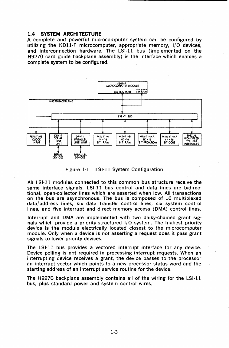
1.4
SYSTEM
A
complete
utilizing
interconnection
and
H9270
card
complete
ARCHITECTURE
and
the
KDll-F
guide
system
H9270
BACKPLANE
powerful
microcomputer,
hardware.
backplane
to
be configured.
microcomputer
appropriate
The
LSl-11 bus
assembly)
LSI
·11
system can be
memory,
(implemented
is
the
interface
BUS
configured
1/0 devices,
which
enables a
on
by
the
SERIAL PARALLEL
DEVICES
All LSl-11
same
tional,
on
data/
modules
interface
open-collector
the
bus are asynchronous. The bus is composed
address lines,
lines, and five
Interrupt
nals
device is
module.
signals
The
Device
interrupting
an
starting
The
bus, plus
and
provide a priority-structured
which
the
Only when a device is
to
lower
LSl-11
bus
polling
device receives a
interrupt
vector
address
H9270
backplane
standard
DEVICES
MSVll·A
11( • 16
SIT RAM
MSV11·8
BIT
Figure 1-1 LSl-11 System
connected
signals. LSl-11 bus
lines
six
interrupt
DMA
are
module
electrically
priority
provides a vectored
is
not
required in processing
which
of
an
interrupt
assembly
power
to
which
are asserted when low. All
data
transfer
and
direct
implemented
not
devices.
grant,
points
to
service
contains
and system
this
common
control
memory
located closest
asserting
interrupt
the
a new processor
41(•16
RAM
MMVll·AA
41(
BIT
Configuration
bus
structure
and data lines are bidirec·
of
control
with
1/0
lines, six system
access
two
daisy-chained
system. The
(DMA)
to
16
highest
the
microcomputer
a request does
interface
interrupt
device passes
for
requests. When an
to
status
routine
for
the
device.
all
of
the
control
wiring
wires.
SPECIAL
HIGH·SPfEO
•16
UO
CORE
INTERFACES
receive
transactions
multiplexed
control
control
grant
priority
it
pass
any
device.
the
processor
word
and
for
the
LSl-11
USER
the
lines.
sig-
grant
the
1-3
Page 11
1.5 MICROCOMPUTER
The
microcomputer
of
location
logic
speed, general-purpose registers which can be used as
address pointers,
processor does both single and
both
directly
cessor
The
The
(microcode
the
operations
16-bit
word and
between
registers.
microcomputer
four
chips
read-only
connected
LSl-11
and
index
1/0
processor is
are
the
memory)
bus
instruction
8-bit
devices and
to
for
peripherals
registers, and
double
byte data. The bus
implemented
control
chip,
chips.
the
LSl-11 bus
decoding.
other
operand
memory
the
and
performs
It
contains
specialized
addressing
without
with
data
chip, and
controls
permits
disturbing
four
Control Chip
This
chip
and
•
• Location
• Return Register
• Data
•
provides
control
Programmable
anism
for
tions.
accesses
Transfer
data/
address port.
Interrupt
cessor
and
the
for
generating
Counter
are
Logic-Provides
four
microinstruction
the
data access port.
Translation
(LC)-Stores
being made.
(RR)-Used
Control
external flags
It
Array
microinstruction
Logic-Provides
control
(PTA)-Provides a decoding
the
address in
to
hold a microsubroutine
over
for
the
address sequence,
contains
addresses
control
three
system.
the
the
microm
and
internal
following
from
timing
flags
Data Chip
The data
microinstructions.
• Register
quired
Arithmetic
•
operations
•
Condition
section.
•
Data/
chip
File-Provides
data.
and Logic
necessary
Flags
Address
incorporates
It
offers
Unit
for
Logic-Monitors
Port-Provides
the
paths, registers, and logic
the
following
multiple
(ALU)-Performs
instruction
registers
the
access
features:
for
execution.
status
to
the
storage
the
of
the
data
arithmetic
result
address lines.
Microm Chips
The
microm
basic
nique)
An
optional
cessor, via a
instruction
chips provide storage
PDP-11/35,40
firmware,
fifth
socket
set
resident
chip
to
include
of
instruction
ASCII/ console routine, and
(third
available on
microm)
fixed
the
set,
resident
the
microcomputer
and
floating
microcode
ODT
(octal
can be added
point
module,
arithmetic
for
bootstrap.
to
the
time
arithmetic
multiple
accumulators,
functions.
and
handles
data
transfers
the
LSI
40-pin
two
microm
for
the
microm
features:
macroinstruc-
from
return
address.
signals
for
the
to
execute
of
frequently
and logic
from
the
emulation
debugging
the
LSl-11 pro-
to
extend
instructions.
al-
and
high-
The
pro-
chips.
mech-
which
for
pro-
re-
ALU
of
the
tech-
the
1-4
Page 12
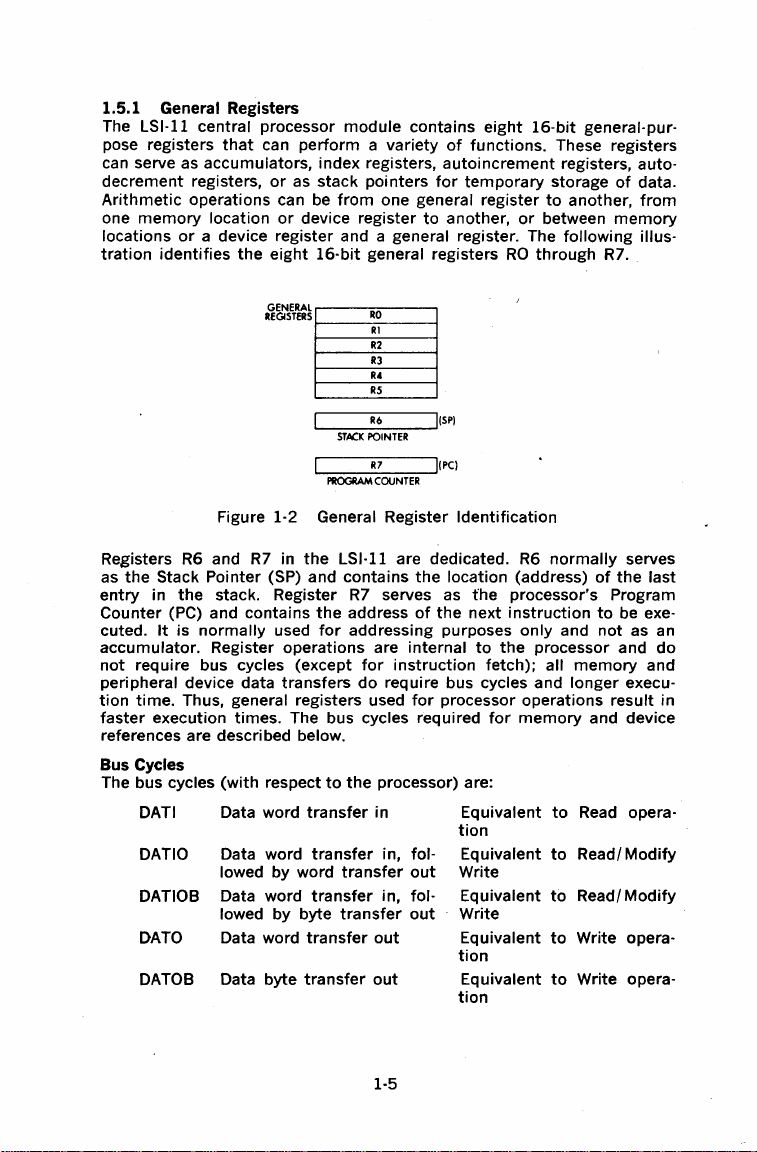
1.5.1 General Registers
LSl-11 central processor
The
pose registers
can serve as
decrement
Arithmetic
one
memory
locations
tration
identifies
that
can
accumulators, index registers,
registers,
or
operations can be
location
or
a device register and a general register. The
the
or
eight
module
contains
perform a variety
as
stack
pointers
from
one general register
device register
16-bit
general registers
eight
of
functions.
autoincrement
for
temporary
to
another,
16-bit
These registers
registers, auto-
storage
to
or
between
following
RO
through
general-pur-
of
another,
memory
R7.
data.
from
illus-
GENERAL
REGISTERS
STACK
PROGAAM
Figure 1-2 General Register
Registers R6 and
as
the
Stack Pointer (SP) and
entry
in
the
Counter (PC) and contains
It
cuted.
is
accumulator.
not
require bus cycles (except
peripheral device data
tion
time.
faster
Thus, general registers used
execution times. The bus cycles required
R7
in
stack. Register
normally
Register
used
operations
transfers
the
LSl-11 are dedicated. R6
contains
R7
the
address
for
addressing purposes
for
do
references are described below.
Bus Cycles
The bus cycles
DATI Data word
DATIO
DATIOB
DATO
DATOB
(with
respect
transfer
Data word
transfer
lowed by word
Data word
transfer
lowed by byte
Data word
Data byte
transfer
transfer
to
the
transfer
transfer
RO
Rl
R2
RJ
R•
RS
R6
POINTER
R7
COUNTER
It
SP)
ltPC)
Identification
the
serves as
are internal
location (address)
of
the
instruction
the
processor's Program
next
instruction
to
the
fetch);
require bus cycles and
for
processor operations result in
for
processor) are:
in
Equivalent
ti
on
in, fol- Equivalent
out
Write
in, fol- Equivalent
out
Write
out
out
Equivalent
ti
on
Equivalent
ti
on
normally
of
to
only
and
not
processor and
all
memory
longer
memory
and device
to
Read opera-
Read/
to
Read/
to
Write opera-
to
Write
to
serves
the
last
be exe-
as an
and
execu-
Modify
Modify
opera-
do
1-5
Page 13
Every processor
instruction
requires one
or
operation required is a DATI, which fetches an
tion
addressed by
referenced in
required
for
however, one
Note
the
which
processor
distinction
may
instructions;
cycles since
the
memory
instruction
or
more
change
these
operations
Program Counter (R7).
or
in an
1/0
execution.
additional
between
the
state
DMA
operations
device, no
If
memory
bus cycles are required.
interrupts
of
the
processor, can
do
not
change
and DMA operations:
can
occur
Addressing Memory and Peripherals
The
maximum
memory.
addressed in
(28K-32K)
dressing. However,
space
to
An
LSl-ll
direct
LSl-ll's
precisely
are
usually
1/0; he can
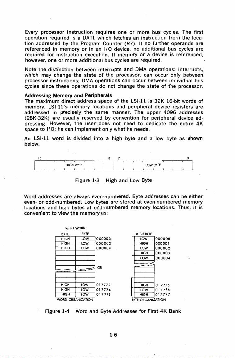
word is
address space
memory
locations
the
same manner. The
reserved by convention
the
user does
implement
divided
only
into
a high byte and a low byte as shown
of
the
LSl-11 is
and peripheral device registers are
not
need
what
he needs.
below.
more
bus cycles. The
instruction
If
no
additional
or
a device is referenced,
further
bus cycles are
from
operands are
Interrupts,
occur
32K
only
individual
of
the
16-bit
4096
the
processor.
addresses
between
the
state
upper
for
peripheral device ad-
to
dedicate
the
loca-
between
words
entire
first
bus
of
4K
15
: HIGH:
BYTE
Figure 1-3 High and Low Byte
Word addresses are
even-
or
odd-numbered. Low bytes are stored
always even-numbered. Byte addresses can be
locations and high bytes
convenient
to
view
the
16-BIT
WORD
BYTE
HIGH LOW
HIGH LOW
HIGH LOW
HIGH
HIGH
HIGH
WORD ORGANIZATION
memory
Figure 1-4 Word and Byte Addresses
:
at
odd-numbered
BYTE
000000
000002
000004
___.-"'.'.
OR
01
LOW
LOW
01
017776
LOW
as:
7772
7774
1-6
7
1
LOW0PifTE:
I I
at
even-numbered
memory
8-BIT
BYTE
LOW
HIGH
LOW
HIGH
LOW
HIGH
LOW
HIGH
t
BYTE
ORGANIZATION
for
First
0
memory
locations. Thus,
000000
000001
000002
000003
000004
01
7775
017776
017777
4K
Bank
either
it
is
Page 14
Certain
and
trap
3768 are
Several
itiated)
1.5.2
memory
of
traps.
The Processor
handling
usually
these
locations
and peripheral device registers. Addresses
reserved
are reserved in
have been reserved by
for
trap
and device
particular
Status
Word (PSW)
convention
interrupt
for
system
for
vector
(processor
interrupt
from O to
locations.
in·
lS
[~=~=~~~~---~~=~=-~---~~~Rl-ORTY~:
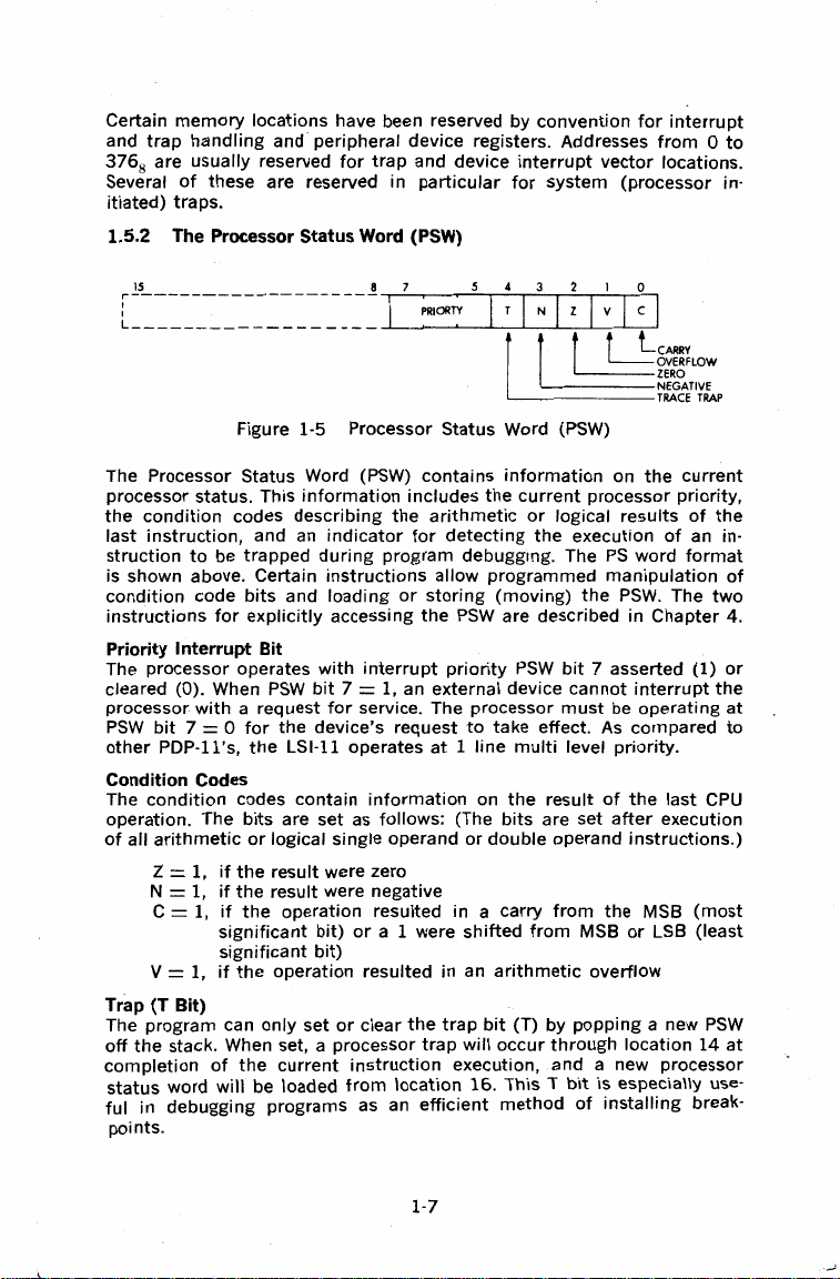
Figure 1-5 Processor Status Word (PSW)
The Processor Status Word (PSW)
processor status. This
the
condition
last
instruction,
struction
is shown above. Certain
condition
instructions
Priority
The processor operates
cleared
processor
PSW
bit
other
PDP-ll's,
Condition
condition
The
operation. The
of
all
arithmetic
Z = 1,
N
C
V = 1,
Trap
(T
The
program
off
the
completion
status
ful
in
debugging
points.
codes
to
be
code
for
Interrupt
(0).
When
with
7 = 0
Codes
if
= 1,
if
=
l,
if
significant
significant
if
Bit)
can
stack. When set, a processor
of
word
will
information
describing
and an
trapped
bits
explicitly
a request
for
the
codes
bits
or
the
the
the
the
the
be loaded
indicator
during
program
instructions
and
loading
accessing
Bit
with
PSW
the
LSl-11
contain
are set as follows: (The
logical single operand
result
result
operation
operation
only
current
programs
interrupt
bit
7 = 1, an external device
for
service. The processor
device's
operates
information
were zero
were negative
resulted in a
bit)
or
a 1 were
bit)
resulted
set
or
clear
instruction
from
as an
the
or
request
location
~r~l_N_l_z~l
)
1
~-
-----NEGATIVE
'---------TRACE
contains
includes
arithmetic
for
allow
storing
the
at 1 line
the
trap
efficient
information
the
current
detecting
PSW
priority
in
trap
execution,
or
debugging. The
to
or
shifted
an
will
the
programmed
(moving)
are described in
PSW
take
effect.
multi
on
the
bits
double
carry
from
arithmetic
bit
(T)
occur
16.
This
method
logical
bit
cannot
must
level
result
are set
operand
from
by
through
and
T
b"1t
0
_v
~I
~c
I
UJ:~'°"
TRAP
on
the
processor
execution
PS
manipulation
the
7 asserted
be
As
priority.
of
after
the
MSB
overflow
popping
a new processor
is
of
installing
current
priority,
results
PSW.
especia\ly use-
of
the
of
an in·
word
format
The
two
Chapter
(1)
interrupt
operating
compared
the
instructions.)
MSB
or
a new
location
last
CPU
execution
(most
LSB
(least
PSW
14
break-
the
of
4.
or
at
to
at
1-7
Page 15
1.5.3
Instruction
Implementing
mits
the
of
with all associated application notes, software,
reliability,
programs.
The
registers
the
puter
usually have
tions, operate
all data
one
ulated
are used
in
register can be tested
into
pare data logically
The basic
address
very efficiently in one step such operations as
operands
user
experience
customer
instruction
to
most
comprehensive and powerful
in
the
manipulation
set
of
as
flexibly
to
peripheral device registers. For example, data in an external device
memory
order
instructions
or
LSl-11 Approach
ADD
Conventional Approach
LOA
ADD B
STA B
Addressing
Much
of
dressing capabilities. LSl-11 addressing modes
ward
bit
able-length
to
gram
the
or
backward addressing, address indexing,
word addressing,
be used
storage space.
Set
the
PDP-11
to
take
with
the
complement
provide
16-bit
three
or
accumulator
instructions.
as
manipulate
or
disturbing
or·arithmetically
code
moving
A,
B
A
power
instruction
for
each addressing mode. The
instruction
advantage
PDP-11
references, and
more
class. Unlike conventional
classes
operations in
memory
data in
or
of
for
an
operand
of
the
8-bit
formatting
of
family-more
uses
than
400
of
instructions
control
Since peripheral device registers can be manip-
by
the
memory
modified
the
general registers. One can add
the
LSl-11 uses both single and
words
or
from
Add
store results
Load
accumulator
Add
cumulator
Store result
LSl-11 is derived
byte addressing, and stack addressing. Vari-
repertoire in
Digital
Equipment
than
17,000
the
the
flexibility
powerful hard-wired
instruction
instructions,
the
central processor,
can be used equally well
directly
in a device register.
bytes. The LSl-11
one location
contents
contents
contents
allows a
documentation,
DECUS
LSl-11 are accomplished
by
at
at
library
of
repertoire
16-bit
(memory
and 1/0
the
CPU
adding
of
location A
location B
of
memory
of
memory
location B
from
its
include
indirect
minimum
result
is efficient use
the
LSI
chip
Corporation's
units
installed,
training,
of
application
the
general-purpose
instructions-
of
computers, which
reference instruc-
without
therefore
or
to
another.
wide range
number
any com-
instructions),
instructions
bringing
or
double
operand
performs
subtracting
to
location
location A
location B
sequential for-
addressing, 16-
of
set per-
years
with
that
for
data
com-
two
into
to
ac-
of
ad-
words
of
pro-
it
B;
1-8
Page 16
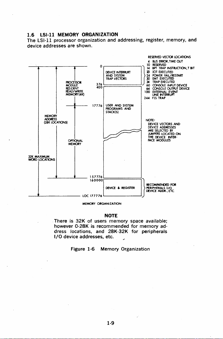
1.6
LSl·ll
MEMORY
ORGANIZATION
The LSl-11 processor organization and addressing, register, memory, and
device addresses are shown.
RESERVED
VECTOR
ERROR,
TIME
TRAP
INSTRUCTION, T BIT
EXECUTED
FAIL/RESTART
EXECUTED
EXECUTED
~~~D~
EVENT
NTERRUPT
TRAP
VECTORS
AND
ADDRESSES
BY
LOCATED
NTER-
ADDR.,
ETC:
LOCATIONS
OUT
1
~1~
ON
32K
MAXIMUM
WORD
LOCATIONS
----''---------
PROCESSOR
MODULE
RESICfNT
READ/WRITE
MEMORY(4K)
~MORY
ADORE
SS
(28K
LOCATIOllS)
OPTIONAL
MEMORY
_......_
___
4
O
~--------.
DEVICE
INTERRURT
AND
SYSTEM
TRAP
VECTORS
!6~
~============:
1 7 7 7 6
USER
AND
SYSTEM
PROGRAMS
STACK(S)
.....__
__
:~~~~~::=========:}
DEVICE & REGISTER
LOC
177776
....__
MEMORY
ORGANIZATION
AND
_____
BUS
10
RESERVED
14
BPT
~
!OT
24
PONER
30
EMT
}
34
TRAP
~
~~
100
EXTERNAL
LINE
244
FIS
NOTE:
DEVICE
DEVICE
ARE
SELECTED
JUMPERS
THE
DEVICE
l'ACE
MODULES
=~=~OFOR
DEVICE
__,
There is
however
32K
of
0-28K
is recommended
users
memory
dress locations, and 28K-32K
NOTE
1/0
device addresses, etc.
Figure 1-6 Memory Organization
1-9
space available;
for
memory
for
peripherals
ad-
Page 17
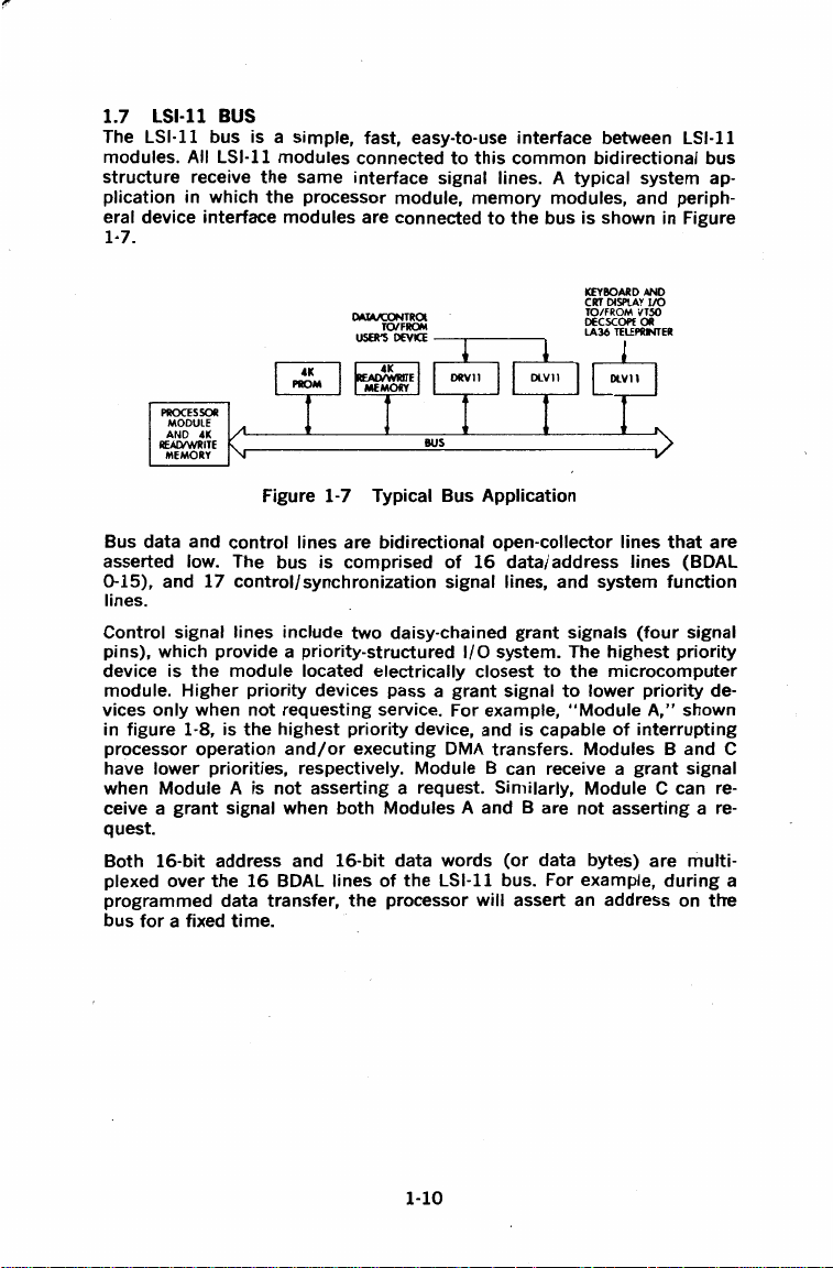
1.7
LSl·ll
The
LSl·ll
modules. All LSl-11
structure
plication
eral device
BUS
bus
receive
in
which
interface
is a
modules
the
the
modules
1·7.
PROCESSOR
MODULE
AND
41(
~ITE
MEMORY
Figure
Bus
data
and
control
asserted low. The bus
0-15),
and
17
control/synchronization
lines.
Control
pins),
device
module.
vices
in
processor
have
when
ceive a
which
only
figure
lower
Module
signal
lines
include
provide a priority-structured
is
the
module
Higher
priority
when
not
the
highest
requesting
and/or
1·8, is
operation
priorities,
A is
signal
not
when
grant
quest.
Both
16-bit
over
a fixed
address
the
16
data
time.
BOAL
transfer,
plexed
programmed
bus
for
simple,
fast, easy-to-use
connected
same
interface
processor
are
OoUAJCONTROI.
TO/FROM
USER'S
4K
PROM
1·7
Typical
lines
are
bidirectional
is
comprised
two
located
electrically
devices pass a
service. For example,
priority
executing
respectively.
asserting
both
Modules A and
and
16·bit
lines
of
the
to
this
signal lines. A
module,
memory
connected
DEVICE
-~--~
Bus
Application
of
16
signal lines,
daisy-chained
1/0
closest
grant
device,
and
OMA
Module
a request.
data
words
the
LSl·ll
processor
will
interface
common
between LSl-11
bidirectional
typical
modules,
to
the
bus
is
shown
KEYBOARD
CRT
DtSPl.AY
TO/FROM VT50
DECSCOPE
LA36
TELEPRNTER
open-collector
data/address
and
system
grant
signal
to
to
signals
The
the
lower
highest
microcomputer
system.
"Module
is
capable
transfers.
of
Modules B and
B can receive a
Similarly,
(or
B are
data
Module
not
asserting
bytes)
bus. For example,
assert
an address
system
and
periph·
in
Figure
ANO
l/O
OR
lines
that
lines
(BOAL
function
(four
signal
priority
priority
A,"
shown
interrupting
grant
signal
C can re·
are
during
on
bus
ap-
are
de·
C
a re·
multi·
a
ttre
1·10
Page 18
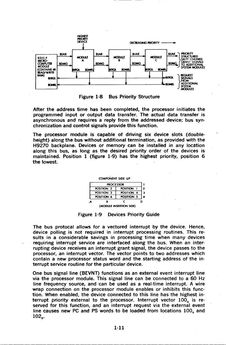
HIGHEST
PRIORTY
DEVICE
DECREASING
FRIORITY
-
~-----.
KDIH
MICRO·
COMPUTER
MODULE
(CO'HAINS4K
READIWRITE
RAM)
After
programmed
asynchronous and requires a
chronization
The
height)
H9270
along
maintained.
the
BIAK
the
address
input
and
control
processor
along
module
the
backplane. Devices
this
bus,
as
Position 1
lowest.
~E
A
Figure 1-8
time
has been completed,
or
output
data
reply
signals
is capable
bus
without
additional
or
long
as
the
(figure
COMPONENT
POSITION 2 POSITION 1
POSITION 3 POSITION 4
POSITION 6
_A
(MODULE
MOOULE
8 .
Bus
Priority
transfer.
from
provide
of
memory
desired
1-9) has
SIDE
PROCESSOI!
POSITION S 4
8
INSERTION
Figure 1-9 Devices
for
The bus protocal
device
polling
sults
in
requiring
rupting
processor, an
contain
terrupt
One bus signal
via
the
is
a considerable savings in processing
interrupt
device receives an
interrupt
a new processor
service
routine
line
processor module. This signal line can be connected
allows
not
service
(BEVNT)
a vectored
required in
are
interfaced
interrupt
vector. The
status
for
the
particular
functions
interrupt
grant
vector
word
and
line frequency source, and can be used
wrap
connection
tion.
When enabled,
terrupt
served
priority
for
line causes new
this
on
the
the
external
function,
PC
and
processor
module
device connected
to
the
words
processor.
interrupt
to
be loaded
and an
PS
1028.
BIAIC
MOOUlE
c
e
Structure
the
processor
The
actual
the
addressed device; bus syn-
this
function.
driving
six device
termination,
can be
UP
C D
Priority
priority
the
highest
SIDE)
installed
order
Guide
interrupt
data
slots
as provided
in
of
the
priority,
by
the
device. Hence,
processing routines. This re-
time
when
along
signal,
points
the
the
the
to
starting
many
bus. When an interdevice passes
two
addresses which
address
device.
as an external event
as
a real-time
enables
to
this
Interrupt
request via
from
or
inhibits
line has
vector
the
locations
interrupt.
the
external event
J
PRIORITY
STRUCTURED
DAISY-CHAINED
WAtiJij8"~
SYSTEM
MODULES
REQUEST
SIGNALS
FROM
ADDITIONAL
}
SYSTEM
MOOULES
initiates
transfer
the
is
(double-
with
any
the
location
devices is
position
6
devices
to
the
of
the
in·
interrupt
to a 60
line
Hz
A wire
this
func-
highest
in·
1008 is re-
1008 and
1-11
Page 19
1.7.1 Bidirectional Lines
With bidirectional and asynchronous
devices can send, receive, and exchange data
bidirectional nature
faces
for
different
1. 7
.2
Communication
has control
ter."
another
relationship is
memory
terface, as master,
control is dynamic. The bus
ample, may pass bus control
ter, could
is a priority
is assigned a
devices which are capable
bus simultaneously,
ceive control.
chronizing
addresses,
processor, as master, is
Master
master-slave relationship. At any
Since
Every device on
1.7.3
Data
independent
slave device. The asynchronous operation precludes
allowed
Full
bus between a
memory, and
struction.
of
The
master
device on
(which is always a slave).
then
the
LSl-11 bus
structure
lnlerlocked
transfer
with, and
to
operate
16-bit
words
or
of
the
devices, and simplifies
Slave Relation
between
the
bus. This
device controls
the
the
processor, as master,
transferring
communicate
the
LSl-11 bus which is capable
priority
Communication
on
the
of
the
at
or
master
data. This
storing
bus allows utilization
two
controlling
bus,
termed
arbitrator
with
is
used by
to
determine
according
of
the
device
LSl-11 bus is interlocked so
physica(bus
waiting
the
maximum
8-bit
bytes
and a slave. The
type
fetching
the
results
communications
devices on
point
in
device is
the
bus when
the
"slave."
Another
data
to
to
becoming a bus
for, clock impulses. Thus, each device is-
of
on
a DMA device. The DMA device,
a slave
the
processor and all
which device
to
its
position
with
the
length and
possible speed.
of
information
information
information
instructions, operands, and data
into
memory
at
their
of
the
interface design.
the
bus is in
time,
there
termed
A typical example
fetching
example is a DMA device in-
memory, as slave. Bus
the
processor module,
memory
higher
bank.
gets
of
becoming bus
along
master
priority
that
the
response
can be transferred on
transfer
after
on
the
LSl-11 bus,
own rates. The
common
is one device
communicating
an
1/0
control
the
request use
communication
the
can be instructions',
execution
bus inter-
the
form
the
"bus
as
devices,
of
the
time
need
for
of
of
master
for
master
of
of
the
instruction
bus. When
position will
occurs when
of
that
mas-
with
this
from
mas-
there
bus.
two
the
the
syn-
the
the
from
a
ex-
re-
is
in-
1-12
Page 20
CHAPTER
2
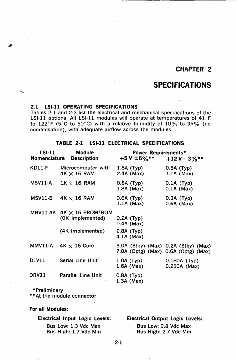
2.1 LSl-11 OPERATING SPECIFICATIONS
Tables 2-1 and 2-2
LSl-11 options. All LSl-11 modules will operate
to
122°F
condensation), with adequate airflow across
Nomenclature
KDII-F
MSVII-A
MSVll-B
MRVll-AA
MMVll·A
DLVll
DRVII
*Preliminary
**At
(5°C
TABLE 2-1 LSl-11 ELECTRICAL SPECIFICATIONS
LSl-11 Module
4K X 16
4K X 16
4K X 16
(OK
(4K
4K x 16
Serial Line
Parallel Line
the
module
list
the
to
50°C)
Description
Microcomputer
lK X 16
RAM
RAM
RAM
PROM/
implemented)
implemented)
Core
Unit
Unit
connector
electrical and mechanical specifications
with a relative
with
ROM
humidity
the
Power
+5 v ±5%**
I.SA
(Typ)
2.4A (Max)
O.SA
(Typ)
I.SA
(Max)
0.6A (Typ) 0.3A (Typ)
l.lA
(Max)
0.2A (Typ)
0.4A (Max)
2.SA (Typ)
4.IA
(Max)
3.0A (Stby) (Max)
7.0A (Optg) (Max) 0.6A (Optg) (Max)
1.0A (Typ)
I.GA (Max)
O.SA
(Typ)
1.3A (Max)
SPECI
at
modules.
Requirements*
FICA
temperatures
of
10%
to
+12V±3%**
O.SA
(Typ)
I.IA
(Max)
0.IA
(Typ)
O.IA
(Max)
0.6A
(Max)
0.2A (Stby) (Max)
0.ISOA (Typ)
0.250A
TIO
of
95%
(Max)
NS
of
41 ° F
the
(no
For all Modules:
Electrical
Input
Bus Low: 1.3 Vdc Max
Bus High: 1.7 Vdc Min
Logic Levels:
2-1
Electrical
Output
Bus Low:
Bus High: 2.7 Vdc Min
O.S
Logic Levels:
Vdc Max
Page 21
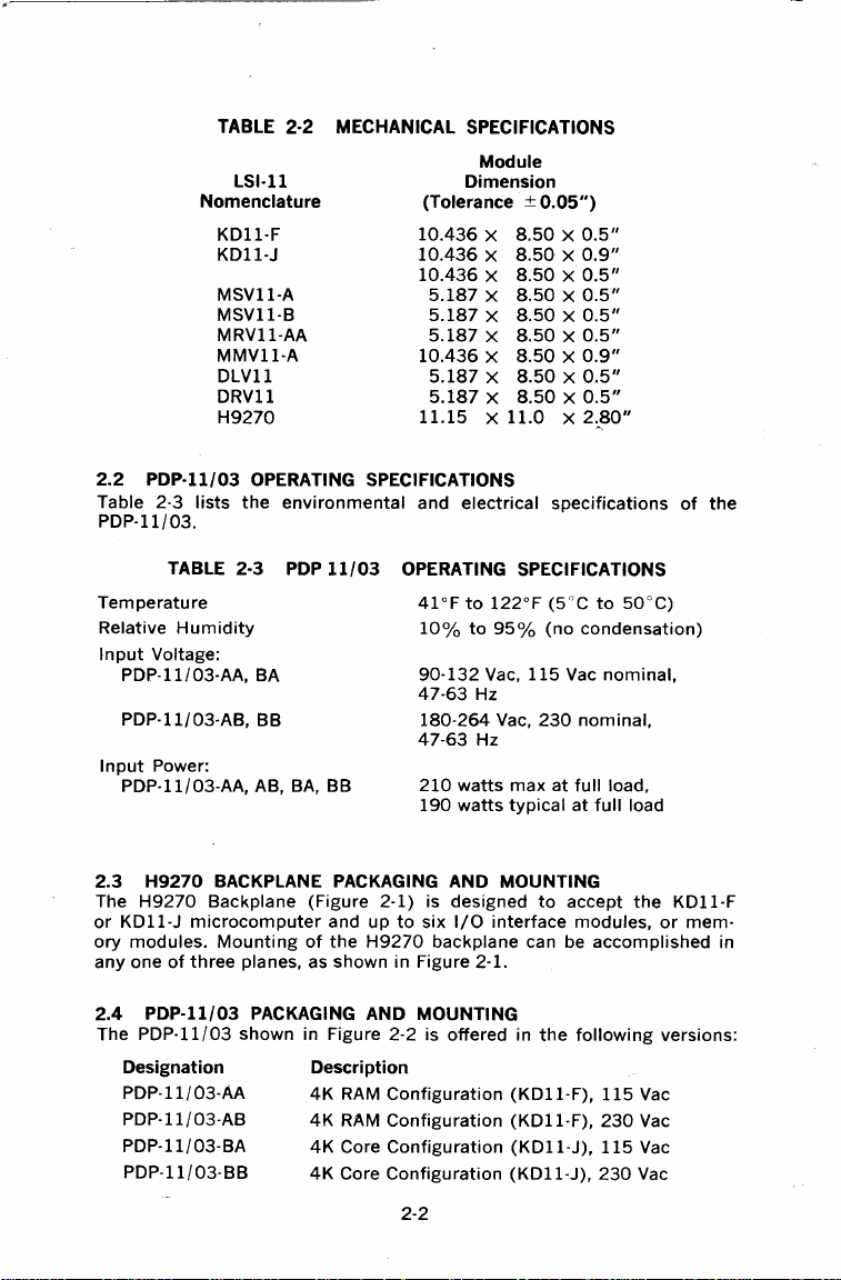
2.2
PDP·ll/03
Table
2·3
PDP·ll/03.
TABLE
2·2
MECHANICAL SPECIFICATIONS
LSl·ll
Nomenclature
KDll·F
KDll·J
MSVll·A
MSVll·B
MRVll·AA
MMVll·A
DLVll
DRVll
H9270
OPERATING SPECIFICATIONS
lists
the
environmental
Module
Dimension
(Tolerance ±
10.436 x 8.50 x 0.5"
10.436 x 8.50 x 0.9"
10.436 x 8.50 x 0.5"
5.187 x 8.50 x 0.5"
5.187 x 8.50 x 0.5"
5.187 x 8.50 x 0.5"
10.436 x 8.50 x 0.9"
5.187 x 8.50 x 0.5"
5.187 x 8.50 x 0.5"
11.15 x 11.0
and
electrical
0.05")
x 2._80"
specifications
of
the
TABLE
Temperature
Relative
Input
Input
2.3
The
or
ory
any
2.4
The
Humidity
Voltage:
PDP-11/03-AA, BA
PDP·ll/03·AB,
Power:
PDP-11/03-AA,
H9270
H9270
KDll-J
modules.
one
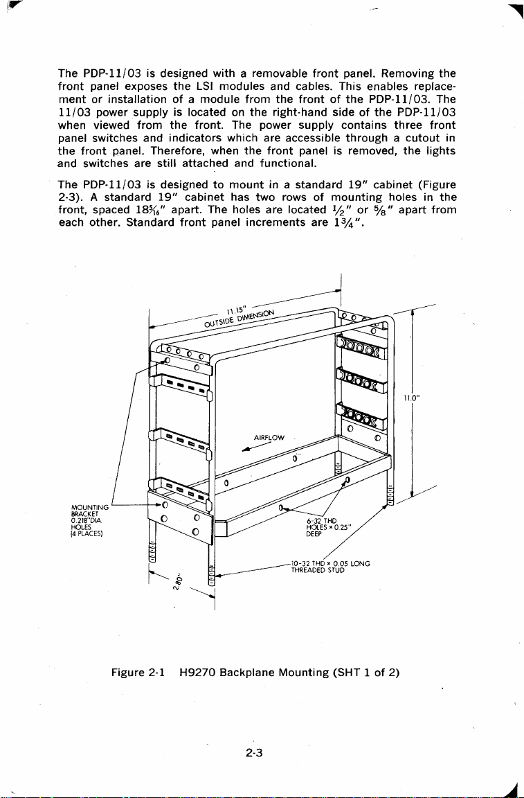
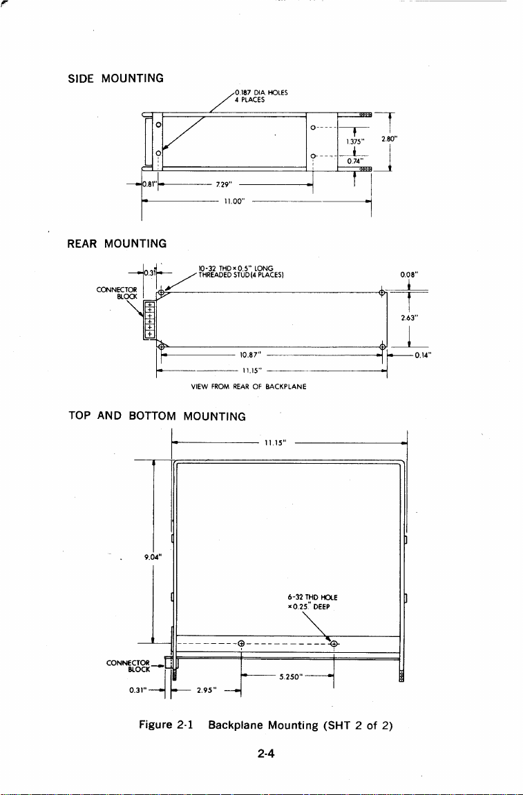
Backplane (Figure 2-1) is designed
microcomputer
of
three
PDP·ll/03
PDP-11/03
Designation
PDP-11/03-AA
PDP-11/03-AB
PDP-11/03-BA
PDP-11/03-BB
2·3
PDP
11/03
BB
AB, BA, BB
OPERATING SPECIFICATIONS
41°F
to
122°F
(5°C
10%
to
95%
(no
condensation)
90-132
47-63
180-264
47-63
210
190
Vac,
Hz
Hz
watts
watts
115
Vac,
max
typical
230
at
Vac
nominal,
full
at
BACKPLANE PACKAGING AND MOUNTING
to
and
up
to
Mounting
of
planes, as shown in Figure 2-1.
the
six
H9270
backplane can be
1/0
interface
accept
modules,
PACKAGING AND MOUNTING
shown in Figure 2-2 is offered in
the
following
Description
4K
RAM
4K
4K
4K
Configuration
RAM
Configuration
Core
Configuration
Core
Configuration
(KDl
(KDl
(KDl
(KDl
1-F),
1-F),
1-J),
1-J),
2-2
to
50°C)
nominal,
load,
full
load
the
KDll-F
or
accomplished
115
230
115
230
mem-
versions:
Vac
Vac
Vac
Vac
in
Page 22
1r
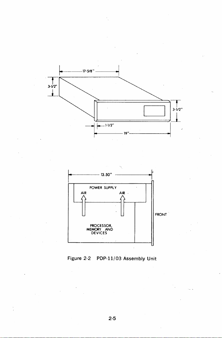
The PDP-11/03 is designed
front
panel exposes
ment
or
11/03
installation
power
when viewed
panel switches and
the
front
panel. Therefore, when
and switches are
supply
from
still
the
LSI modules and cables. This enables replaceof a module
is located on
the
front.
indicators
attached and
The PDP-11/03 is designed
2-3).
A standard
front,
spaced 18Yi
each other. Standard
19"
cabinet
apart. The holes are located If2"
"
6
front
with
a removable
from
the
the
The power
front
right-hand side
supply
which are accessible
the
front
functional.
to
mount
in a standard
has
two
rows
panel
increments
front
panel. Removing
of
the
PDP-11/03. The
of
the
contains
through a cutout
panel is removed,
19"
of
are
cabinet
mounting
or
1 % ".
holes in
% "
the
PDP-11/03
three
front
the
lights
(Figure
the
apart
from
in
MOUNTING
BRACKET
0.218"DIA
HOLES
(4
PLACES)
Figure 2-1
H9270
Backplane
2-3
Mounting
(SHT 1
of
2)
Page 23
SIDE MOUNTING
REAR
MOUNTING
OCNNECT
0.31
~
BLOCK
...
I . -
0.187
DIA
HOLES
4
PLACES
10-32 THDx0.5"
' -
/T"'EADEDSTUO{HCACESJ
t
/ I
LONG
~
i
'~-1~;~1:"··
VIEW
FROM
REAR
TOP AND BOTTOM MOUNTING
I·
9.04"
----
-----9-
Figure 2-1 Backplane Mounting (SHT 2
-==--0"
OF
BACKPLANE
11.15"
THD
HOLE
6-32
xo.25"
DEEP
----
- - - -
5.250"
--:@-
of
2)
' !
2-4
Page 24
.j
l....t:::========:lj
f--1·1/2"
-
i
13.50"
19"------~
r
POWER
PROCESSOR,
MEMORY
DEVICES
SUPPLY
AND
AIR
/I
-
·
~
AIR
/\
.....__
-
Figure 2-2 PDP-11/03 Assembly
C=:J
.
FRONT
Unit
IT
3-112"
_l
2-5
Page 25
FRONT
VIEW
0
o--z---------
TOP
Q
0
0
0
0
0
-------18-5/16"-------
OF A STANDARD
FRONT
PANEL
3-112" 0 +
l
114"
Q T
_1_1_
a
~r
T 518"
1-3/4" 0 +
---
l
------
518"
0 t
518"
0 +
5/8"
9
*·
0
_k
..
l---
~,--~.-.-r-----------------,.-.:
3.50" 1.75"
~
~
1
~._•.....__
T
3.50'
_l__.____
FRONT
_____________
____
18-5/16''-------L.19"
OF
BOX(
PANEL
19"
REMOVED)
~13~"
Figure 2-3 PDP-11/03 Cabinet
2-6
114"
TYP
TYP
TYP
-u--~3/8"
__..___.ci:I
FRONT
t-_
~
~.,..
Mounting
Page 26
CHAPTER
3
Data stored in
dling
is specified by an
usually indicates:
function
• The
• A general-purpose register is
and
and/or
destination operand.
•
An
addressing mode
be used).
A large portion
(in character strings, arrays, lists, etc.).
vide
for
efficient and flexible
The general registers
following ways:
•
As
accumulators. The data
ister.
• As pointers. The contents
rather
As
pointers which
•
matically
autoincrement
as autodecrement addressing. These modes are
processing
•
As
index registers. In
the
word
-
-Of
the
An
important
with
the
• Six general-purpose registers (RO -
• A hardware Stack Pointer (SP), register (R6)
• A Program Counter (PC}, register (R7)
Registers
use is determined by
• They can be used
registers can be added and stored in
• They can contain
the
address
• They can be used
• They can be used as index registers
access.
memory
(operation code).
a general-purpose register
of
than
the
stepping
tabular
following
operand. This allows easy access
LSl-11 feature, which should be considered in
addressing modes, is
RO
through
o!
an operand.
must
LSl·ll
(to
specify how
the
data handled by a
handling
may
be used
operand itself.
automatically
addressing;
the
for
of
forward
or
the
the
for
automatically
array data.
this
instruction
RS
are
not
instruction
operand storage. For example,
address
the
autoincrement
be accessed and manipulated. Data han·
instruction
to
be used when
the
LSl-ll's
of
structured
with
to
be manipulated resides
the
register is
step
through
instance,
the
through
consecutive locations is known as
the
are
summed
register arrangement:
RS)
dedicated
that
is decoded:
another
of
an operand
for
3·1
ADDRESSING
(MOV, ADD, etc.), which
locating
to
be
used when
selected register(s)
computer
an
stepping
contents
to
to
or
convenient data and program
is usually
addressing modes pro-
data.
instruction
the
address
memory
backwards is known
particularly
of
to
produce
variable entries in a list.
any specific
register.
or
serve as pointers
autodecrement
MODES
the
source aper·
locating
is/are
structured
in any
within
of
lo~ations.
the
function;
contents
of
the
reg-
the
operand,
Auto·
useful
register and
the
address
conjunction
their
of
two
features.
the
to
the
for
to
Page 27
The LSl-11 also has
itate
temporary
handling
stack
tion
pointer"
with
R6 as a
ferred
• The
• The
• The hardware
Register
recommended
Whenever an
is
word.
The
• Single Operand
• Double Operand
•
• Deferred
• Use
• Use
•
of
data
manipulation.
is
known as
under
subroutine
"hardware
to
as
the
stack
stack
moves
up
of
the
stack.
information
R7
automatically
next
section is
register;
registers;
operands.
Direct
ister.
is
general-purpose registers in one
processor retrieves an
by 2. By
of
-immediate,
operations.
Summary
the
Addressing-The
(Indirect)
the
address
of
the
combining
the
basic
of
Stack
of
Instruction
bols are
programs. The
cerned
is
program.
instruction
data
storage
which
The
the
stack
program
linkage and
stack
"SP":
pointer
as
is used by
(SP) keeps
pointer
the
moves down as
items
stack
allowing
that
R7
instruction
incremented
divided
Addressing-One
second
Addressing-part
remaining
of
the
PC
as a General
addressing
absolute, relative, and relative deferred.
Pointer
Addressing
sufficient
about
accomplished
structures.
must
register
pointer.
control;
interrupt
pointer."
are removed. Therefore,
is used
the
processor
the
processor as
not
be used as a
is fetched
into
part
provides
parts
operand is
Addressing-The
operand.
instruction,
this
automatic
modes, we
as
General
Modes
mnemonics
programmer
conversion
automatically
addressing
be
frequently
used
to
Any
however,
service
For
track
of
items
during
trap
to
from
by
two
to
seven
major
part
information
of
provide
the
Register-The
important
it
advancement
produce
Register-Can
NOTE
and address
for
writing
to
mode
This can be used
register
this
the
return
of
the
contents
combinations
accessed. This is known as
keep
track
can be used as a
certain
its
automatically
assembly
instructions
automatically
reason, R6 is
latest
are added
it
always
or
interrupt
to
the
program
stack
pointer
memory,
point
to
categories:
the
instruction
for
instruction
information
contents
of
PC
respect. Whenever
the
four
mode
need
not
binary
digits;
by
the
for
of
stack
use Register
frequently
entry
on
to
the
points
handling
main
counter
or
the
the
locating
the
is
language
assembler
accumulator.
program
next
word specifies a
word specifies
for
of
the
selected reg-
selected register
unique
advances
of
the
special
be used
sym-
be con-
this
the
program.
the
locating
PC
that
facil-
convenient
manipula-
"stack
associated
re-
stack.
stack
and
to
the
top
to
store
(PC).
It
counter
instruction
operand.
the
two
from
other
the
the
PC
with
four
PC
modes
for
stack
is
3-2
Page 28
3.1 SINGLE OPERAND ADDRESSING
The
instruction
increment,
test)
format
is:
for
all single operand
instructions
(such as clear,
15
OP
CODE---~
DESTINATION
Bits
15
struction
through
to
Bits 5 through 0 form
This consists
a)
Bits O through
is
to
be referenced by
b) Bits 3
through
dress mode).
3.2
DOUBLE OPERAND ADDRESSING
Operations which
compare) are handled by
first
operand is called
operand.
may
format
Bit
specify
for
the
15
SOURCE
DESTINATION
ADDRESS----------~
6 specify
be executed.
a six-bit field called
of
two
subfields:
2 specify which
5 specify how
Bit 3 is·
imply
two
the
assignments in
different
modes and
double operand
OP
CODE
11
12
ADDRESS~--~
ADDRESS-------------'
the
this
set
instructions
source operand,
MODE
10
6 5 4 3 2
operation code
of
the
instruction
to
indicate deferred
eight
word.
the
selected register will be used (ad·
MODE
that
the
destination address field.
general purpose registers
Rn
defines
(indirect)
0
the
type
addressing.
of
in·
operands (such as add, subtract, move and
that
specify
the
source and destination address ffelds
different
instruction
9 8 6 5 4
is:
Rn
two
the
second
registers. The
MOOE
addresses. The
the
destination
Instruction
Rn
0
The source address field is used
to
select
the
source operand,
operand. The destination is used similarly, and locates
erand and
contents (source operand)
operand)
addition and
the
result. For example,
of
location
the
B.
contents
the
of
location A
After
execution B will contain
of
A will
instruction
be
unchanged. ·
to
ADD
the
contents (destination
3-3
the
A,
the
the
second op-
B adds
result
of
first
the
the
Page 29
Examples in
this
section and
further
sample LSl-11 instructions. A complete
is located in
the
appendix.
in
this
listing
chapter
-0f
the
use
LSl-11
the
following
instructions
Mnemonic
CLR
CLRB
INC
INCB
COM
COMB
ADD
DD
= destination field
SS
=
sourc~
)
=contents
, Description Octal Code
clear (zero
clear byte (zero
the
specified
the
destination)
increment
increment
(add 1
to
byte (add 1
destination byte)
complement
destination by
each 0
complement
destination
each 0
(replace
their
bit
is set and each 1
byte (replace
byte by
bit
is set and each 1
add (add source operand
operand and store
the
address)
(6
bits)
field
(6
bits)
of
destination)
byte in
the
specified 1050DD
contents
the
to
the
contents
of
destination)
~ntents
of
the
logical complement;
bit
is cleared)
the
their
contents
logical complement;
bit
is cleared).
to
destination 06SSDD
result at destination
of
of
the
0050DD
0052DD
1052DD
0051
DD
1051DD
3-4
Page 30
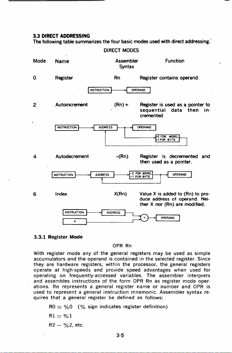
3.3
DIRECT
ADDRESSING
The following table summarizes the four basic modes used with direct addressing.-
Dl
RECT
MODES
Mode
0
2
4
6
3.3.1
Name
Register
Autoincrement
INSTRUCTION ADDRESS
Autodecrement
INSTRUCTION
Index
:
'"'7"0N
Register
With register
accumulators
they
are
operate
operating
hardware registers,
at
high-speeds and provide speed advantages when used
on frequently-accessed variables. The
and assembles
Rn
ations.
used
quires
represents a general register
to
represent
that
a general register be
RO=
%0
Rl = %1
R2 -%2,
Mode
mode
any
and
the
instructions
a general
(%
etc.
Assembler Function
Syntax
I
1NSTRUCTION
Rn
~
(Rn)+
Register contains operand
OPERAND I
Register is used
sequential
as
data
a pointer
then
to
in-
cremented
-(Rn)
ADDRESS
X(Rn)
Register is decremented and
as
then used
-2
FOR
WORD,
-1
FOR
BYTE
Value X is added
duce address
a pointer.
OPERAND
to
(Rn)
of
operand. Nei-
to
pro-
ther X nor (Rn) are modified.
~r-----A-00-R-ES-S-~~
OPR
of
the
operand is
general registers
contained
within
the
Rn
processor,
+
_OPE_R_AN_O__.
may
in
the
be used as
selected register. Since
the
general registers
simple
for
sign
of
the
instruction
defined
indicates
form
register
OPR
Rn
name
or
mnemonic.
as follows:
definition)
assembler
as
register
number
Assembler
interprets
mode
and
OPR
syntax
oper-
is
re-
3-5
Page 31

Registers are typically referred
R6
and R7. However
R6
and
respectively.
Register Mode Examples
(all numbers in octal)
to
by name as
R7
are also referred
RO,
Rl,
R2, R3,
to
as
SP
R4,
and
R5,
PC,
Symbolic
INC
1.
R3
Operation:
._l_o_._o_.._o_.__o_.__.._o_.___.._o_.._,__o~j_o_.._o_._)_o~l~o-·....__._~1
~·---~~-----6-
OP
CODE
(INC(0052))_J
DESTINATION
2.
Operation: Add the contents of
FIELD-----------~
ADDR2,R4
R4
BEFORE
R2
._I
__
...
I
__._o_ooo_04
Octal Code
005203
Add one
to
'-5
060204
00000
__
2~
__
Instruction
Increment
the
contents
4 3 2 0
Add
R2
to the contents of
AFTER
R2
._I
__
0_0_000_2__,,
R4
._I
__
o_oo_o_o_s__,,
Name
of
general register 3
R0
RI
R2
..
l~~~~R
R3
R4
~·
R5
R6(SP)
R7 (PC)
R4.
3. COMBR4
Operation:
BEFORE
R4
I 02<!222
105104
One's complement bits 0-7 (byte) in
Complement Byte
R4.
(When
general registers are used, byte instructions only
operate on bits 0-7; i.e. byte 0 of the register)
AFTER
R4 I
022155
3-6
Page 32

3.3.2 Autoincrement Mode
OPR
This mode provides
tial
elements
selected general register
registers are stepped
two
for
R6 and R7)
of
for
a table
(by
to
automatic
of
operands.
to
be
the
one
for
address
the
increment mode is especially useful
cessing.
address
handling,
of
It
the
this
purposes.
will access an element
next operand in
of a table
the
mode is completely general and may be used
(Rn)+
stepping
address
bytes, by
table. Although
of a pointer
It
assumes
of
the
two
next
sequential location. The auto-
for
array processing and stack pro-
and
then
through
the
contents
operand. Contents
for
words, always by
step
most
useful
the
for
sequen-
of
pointer
for
table
a variety
the
of
to
Autoincrement Mode Examples
Symbolic Octal
CLR
1.
(R5)+
Operation:
BEFORE
ADDRESS
20000
30000
2.
~
SPACE
I
005025
I 111!11s I
CLRB(R5)+
I
R5
I
Operation:
BEFORE
AIDRESS
SPACE
20000
I
105025
I R5 I
Code
Instruction Name
005025 Clear
Use
contents
of
R5
as
the address of the operand.
Clear selected operand and then increment the
contents
REGISTER
of
030000 I 20000
30000
R5
by
AFTER
ADDRESS
two.
005025
000000
SPACE
REGISTER
R5
__
I
__
03_0_00_2_
105025 Clear Byte
Use
contents of
Clear selected byte operand and then increment
the contents
REGISTER
030000
I
20000
of
R5
R5
AFTER
ADDRESS
as
the address
by one.
SPACE
105025
of
the operand.
REGISTER
R5
l....__0_3_00_0_1 ____.
30000~
30002~
:=
3-7
1-1-11__._oo_o_
Page 33

3.
ADD(R2)+,R4
062204
Add
Operation:
The contents
operand which is added
is then incremented
REGISTERS
3.3.3
Autodecrement Mode (Mode
This
mode
is
useful
for
The
contents
for
word
the
address
features
to
facilitate
of
the
instructions,
of
the
for
the
LSl-11 were
hardware/software
processing
selected general
by one
operand. The choice
Autodecrement Mode Examples
1.
Operation:
Symbolic
INC-(RO)
Octal Code
005240
The
and used as
operand is
of
R2
AFTER
AOORESSSIW:ES
10000
I
1000021
4)
OPR-(Rn)
data
in a list
register
for
byte
instructions)
of
not
arbitrary
postincrement,
decisions,
stack operations.
contents
of
the
incremented
are used as the address
to
the contents
by
two.
REGISTERS
062204
010000
are
in
reverse
decremented
and
112
R4 I
I
then
100004
020000
predecrement
but
were
Instruction
Name
Increment
RO
are
address
decremented
of
the
operand. The
by
one.
of
the
of
R4.
R2
direction.
(by
two
used as
intended
by
two
BEFORE
ADDRESS
,
ooo
I
11114
I
2.
Operation:
SPACE
005240
000000
INCB-(RO)
REGISTERS
RCil I 017776
17774
105240 Increment Byte
The contents
as
used
byte is increased
the address
3-8
AFTER
ADDRESS
1000 I 005240
~
jOOOOot
of
RO
are decremented by one then
of
by one.
Re I
REGISTER
017774
SPACE
the operand. The operand
Page 34

BEFORE
AOORESS
1000 I 105240
SPACE
REGISTER
RGI I 017776
1000
AFTER
ADDRESS
I 10!1240
SPACE
REGISTER
177741
17776
._
3.
Operation:
10020 I 064300
:::
.... , __
3.3.4
Index
The
contents
struction word, are summed
the selected register may
allowing random access
thus
can then
structions are
in
the memory location following the instruction word and
register.
eral
Index
Mode Examples
000
000
_ ___.
____
ADD-(R3),RO
ADDRESS
SPACE
ooooso
__
Mode
of
the selected general register, and
be
modified
of
Symbolic
_
Rf)
R3 _,
_
(Mode
by
the form
to
the contents
10020 I 064300
__
Add
of
R3
AFTER
AOORESSSPACE
to
064300
The contents
used as a pointer
added
REGISTER
I
000020
__
r:n_1_11_&
6)
OPR
X{Rn)
to
form the address
be
used
as
a base
to
elements
program
OPR
X(Rn) where X is the indexed word and is located
Octal
to
access data
Code
of
~n
of
for
calculating a series
data structures. The selected register
in
Instruction Name
are decremented by 2 then
an operand (source) which is
of
RO
(destination operand).
REGISTER
Rf)
I
0000010
index word following the in·
the operand. The contents
of
addresses,
the table. Index addressing in-
Rn
is the selected gen-
of
1.
Operation:
CLR
200{R4)
005064
000200
address
The
adding
and
location
200
3.9
Clear
of
to
the
is
then
the
operand
contents
cleared.
is
determined
of
R4. The oper-
by
Page 35

BEFORE
AOORESS
SPACE
R4
1020~05064
1022
000200
1024
~
/
a
1200
1202
l..___oo_•ooo
.+200
__
REGISTER
!000
1200
__
_,
1020
1022
1024
AFTER
ADDRESS
005064
000200
SPACE
R4
..
I
__
REGISTER
0_0_10_0_0 _ _,
COMB
2.
200(Rl)
Operation:
BEFORE
ADDRESS
SPACE
1020
1022
105161
000200
~---------
201761
20200
3.
011!000
I
ADD
30(R2),20(R5) 066265
Operation:
BEFORE
ADDRESS
SPACE
1020~265
1022
000030
1024
000020
105161
000200
The contents
adding 200 to the contents
(i.e. logically complemented)
1020
!022
201761
20200
I
RI
plemented.
REGISTER
017777
01777 7 +200
-020177
000030
000020
The contents
adding 30 to the contents
of
contents
a location which is determined
ding 20 to the contents
at
the destination address, i.e, 20(R5)
REGISTER
R2 I 001100
R5 I
002000
1020
1022
1024
Complement Byte
of
a location which is determined
AFTER
ADDRESS
105161
000200
166:000
SPACE
of
Rl
are one's com-
RI I
REGISTER
Add
of
a location which is determined
AFTER
ADDRESS
066265
000030
000020
of
SPACE
of
R5.
R2
are added
The
R2
R5
result
REGISTER
l,___0_0_11_00 _
l._
__
017777
is
00_20_00
to
by
stored
__,
_ _.....
by
by
the
ad·
1130 I
2020 1
1100
+30
li30
000001
000001
2000
+20
2620
3-10
1130 I
2020
000001
000002
I
Page 36

3.4
DEFERRED (INDIRECT) ADDRESSING
four
The
in
In
address
In
the
are therefore used when a table consists
ands. Assembler syntax
"(
deferred versions
Mode Name Assembler' Function
basic modes may also
the
register mode
the
register deferred mode
of
the
operand.
the
three
address
)"
1
other
of
the
when
this
is
of
Register Deferred
the
deferred modes,
operand rather
not
the
I
be
operand is
for
ambiguous). The following table summarizes
basic modes:
INSTRUCTION
used with deferred addressing. Whereas
the
the
indicating deferred addressing is
@Rn
contents
contents
the
contents
than
the
Syntax
or
(Rn)
1------f
OPERAND
of
the
of
the
operand itself. These modes
of
addresses rather than oper-
Register contains
of
the
selected register.
selected register is
of
the
register selects
operand
I
the
the
"@"(or
the
address
3 Autoincrement Deferred
I
WST~~·
5 Autodecrement Deferred
I
1NSTRUCTION
7
1------f
Index Deferred
WST,.,XCTOON
-:
---~~------~~
:
1------f
AO'
H
'°j"'
1------f
AOORESS
@(Rn)
T._
@-(Rn)
-2
@X(Rn)
~
3-11
+ Register is
pointer
the
address
then incremented (always by
2; even
__
AOO_R-ES_S_~_
Register is decremented (al-
ways by two; even
structions) and then used as
pointer
a
the
address
T
Value X (stored in a word following
(Rn) are added and
is used as a
word containing
of
the
(Rn) are modified.
'
+
ADDRESS
first
to
for
to
ADDRESS
the
operand. Neither X
H
used as a
a word containing
of
the
operand,
byte instructions).
•2
~~
~
for
byte in-
a word containing
of
the
operand.
1------f
instruction)
the
pointer
the
OPERAND
OPERAND
address
and
sum
to
nor
. I
a
Page 37

The following examples illustrate the deferred modes.
Register Deferred Mode Example
Symbolic
CLR @R5
Operation:
Octal Code
005015
The contents
Instruction Name
Clear
of
location specified in
cleared.
BEFORE
::
11---000-1-00--
ADDRESS
SPACE
R5
..
I __
REGISTER
00_1_1_00 _ __.
AFTER
AOORESS
SPACE
::
1--00000--0--
R5
are
REGISTER
Rlj
1
__
00_1_1_00
___
Autoincrement Deferred Mode Example (Mode
Symbolic Octal
INC@(R2)
Operation:
BEFORE
ADDRESS SPACE
1010~
1012~
+
R2
Code
Instruction Name
005232 Increment
The
contents
address
Operand
cremented
REGISTER
010300
of
of
the operana.
is
increased
by
2.
R2
AFTER
ADDRESS SPACE
1010~
1012~
10300
,l-
__
Autodecrement Deferred Mode Example (Mode
Operation:
BEFORE
10100
l--°'-23_45
10102 •
Symbolic
COM
@·(RO)
ADDRESS SPACE
__
Octal
005150
The
then used
erand. Operand
cally
REGISTER
R0 l
__
o 1_0_11_s_
Code
Complement
contents
of
RO
as
the address of the address
is
one's complemented. (i.e. logi-
complemented)
AFTER
ADORESS
.....
~:,.
3)
are
used
as
the address
by
one. Contents
R2 I
00_1_01_0
_~
5)
are decremented
SPACE
,
of
R2
REGISTER
010302
by
two and
of
REGISTER
the
of
is
the ·
in-
op-
10774
·~
__
____
10776
0_10_100
__
___,
.-
;~;:
1
010100
I
3-12
Page 38

Index Deferred Mode Example (Mode 7)
Symbolic Octal Code Instruction Name
ADD@
1000(R2),Rl 067201
001000
Operation:
1000 and contents
the address of the address
the contents
the result
BEFORE
ADDRESS
SPACE
1020
067201
1022
1024
1050 I 000002
3.5
Although
as
program
is
word
tion
the
The
there
for
utilizing
mediate
001000
I
11~0
001050
'-c===:l
~1100
USE
OF
THE
Counter
instruction
still
incremented
of
position
PC
PC
to
incremented
to
these modes
these
Register 7 is a general purpose register,
the
Program
counter
automatically
of
the
to
be executed. (When
PC
is
PC
responds
are
four
handling
the
deferred),
REGISTER
001234
R1
I
000100
R2 I
1000
_+100
AS
A GENERAL REGISTER
for
the
acquire
a word
by
being
executed
the
by
all
the
standard
independent
modes
relative and relative deferred, and are
below:
Mode
Name
Assembler
Syntax
2
Immediate
Absolute
3
Relative
6
7 Relative Deferred
#n
@#A
A
@A
Add
of
which are added to contents of
is
stored in
AFTER
AOORESS
1020
067201
1022
001000
1024
000002
10501
001050
1100 I
LSl-11. Whenever
from
to
or
memory,
contain
the
uses
two
program
two.)
LSl-11
with
are
which
code
termed
addressing
the
and
immediate,
Operand
Absolute
follows
Relative Address
follows
Index
word
is
address
3-13
of
R2
are summed to produce
of
the source operand
Rl.
SPACE
R1
I
R2
I
it
doubles
the
processor uses·
the
address
PC
to
program
of
the
locate
the
address
the
modes. However,
PC
can
provide
unstructured
absolute
Function
follows
Address
instruction
the
instruction.
value
of
the
(stored
the
operand.
following
the
relative address
REGISTER
001236
000100
in
function
counter
of
the
instruc-
byte
next
data,
next
advantages
data. When
(or
summarized
instruction
of
operand
(index
value)
in
instruction)
for
the
Rl;
the
im-
the
Page 39

The reader should
modes described in
the
program counter.
remember
3.3
and 3.4,,
When a standard program is
ful
to
be able
LSl-11 's can accomplish
through
using
the
moved in such a way
altered,
in memory. Thus,
to
load
the
use
of
PC
the
position
addressing modes.
same
offset
PIC
it
into
the
that
relative
usually
location.
The
PC
also
particularly
3.5.1
Immediate
greatly
true
of
Mode
faciiitates
the
immediate
OPR
#n,DD
that
the
special
but
the
available
different
relocation
independent
If
an
the
relative distance between
to
the
references
the
handling
PC
general register selected is R7,
for
different
areas
of
memory
of
a program very efficiently
code (PIC) which is
instruction
PC
can be used in all positions
locations
of
unstructured
and relative modes.
modes are
users,
it
and run
and
its
relative
the
same as
often
is help-
it
there.
written
operands are
them
is
not
to
the
current
data. This is
by
Immediate mode is equivalent to using the autoincrement mode with the
provides time· improvements for accessing constant operands
constant in the
Immediate
Mode
Symbolic
ADD #10,RO
memo..Y
location immediately following the instruction word.
Example
Octal Code Instruction Name
062700
Add
by
including the
000010
Operation:
The value 10
is
located in the second word
instruction and is added to the contents
Just before this instruction is fetched and
1020
1022
1024
BEfOA~
ADDRESS
062700
000010
SPACE
""'R0
REGISTER
I
PC
cuted, the
struction.
increments the
mode is
is used
ond word
cremented
000020
PC
points to the first word
The
processor fetches the first word and
PC
by
two.
The
27 (autoincrement the
as
a pointer to fetch the operand (the
of
the instruction) before being in·
by two to point to the next instruction.
AFTER
ADDRESS
SPACE
>Oro~
1022
000010
1024
source operand
PC).
~I
PC
....-----
Thus, the
REGISTER
000030
of
3-14
PC.
of
the
of
RO.
exe-
the in-
PC
sec-
It
Page 40

3.5.2 Absolute Addressing
QPR
@#A
This mode is the equivalent
ing the
PC.
The
contents
of
immediate deferred
of
the location following the instruction
address of the operand. Immediate data
(i.e.,
an
address that remains constant no matter where in memory the
sembled instruction is executed).
Absolute Mode Examples
Octal
Code
005037
1.
Symbolic
CLR@#llOO
001100
Operation:
2.
BEFORE
ADDRESS
SPACE
005037
20
001100
22
177777
1100
I
1102
ADD@#2000,R3
Clear the contents
PC
063703
002000
or
autoincrement deferred
is
interpreted
Instruction Name
Clear
of
location 1100.
AFTER
ADORES$
20
22
24
1100 I
1102
are
as
an absolute address
005037
001100
000000
taken
SPACE
/PC
as
us-
the
as--
Operation:
BEFORE
ADORES$
000300
SPACE
""R3
Add contents of location 2000 to
AFTER
2000
ADDRESS
20
22
24
I
REGISTER
000500
l
PC
3-15
063703
002000
000300
SPACE
/PC
R3.
R3 l
REGISTER
001000
Page 41

3.5.3 ·Relative Addressing
X is the location
, where
QPR
A
or
of
A relative to the instruction.
OPR X (PC)
This mode is assembled
as
index mode using
lation, which is stored in the second
dress
of
the operand, but the number which, when added
of
the address
code (see Chapter
PC.
When instructions are
the operand. This mode is useful for writing position independent
5)
since the location referenced is always fixed relative to the
to
be
amount.
Relative Addressing
Example
Symbolic Octal Code Instruction Name
INC A 005267 Increment
000054
Operation:
1020
1022
1024
1026
BEFORE
ADDRESS
1---oo_s2_61
000054
SPACE
__
To increment location
tion immediately following instruction word are
ded
are increased by one.
~,
PC
,,~,.,~
or
third word
The base
of
of
the address calcu-
the instruction, is
to
the (PC), becomes
not
the
R7.
relocated, the operand is moved by the same
A,
contents
of
memory loca-
ad-
to
(PC) to produce address
AFTER
1020
1022
1024
1026
t024
1100
I
ADDRESS
0005267
000054
000001
SPACE
A.
Contents
-Pc
of
ad-
A .
3.5.4 Relative Deferred Addressing
OPR@X(PC), where x is'l!ocation containing address
This mode is similar
to
the relative mode, except
struction, when added to the
and, rather than the address
Relative Deferred
Mode
Example
OPR@A
struction.
PC,
contains the address
of
the operand.
or
that
Symbolic Octal Code Instruction Name
CLR@A
005077
Clear
000020
·Operation:
Add
PC
to
Clear
second
produce
operand.
word
address
3-16
of
A,
relative
the second word
of
the address
of
instruction
of
address
to
the in-
of
of
the oper-
to
updated
of
operand.
the in-
Page 42

(PC•102011020
1022
(PC•I02211024
BEFORE
ADDRESS
005077
000020
SPACE
1020
1022
1024
AFTER
ADDRESS
005077
000020
SPACE
"-Pc
IO~IO~ri
~
I
10100
3.6
USE
OF STACK POINTER
The processor stack
register used
decrement with Register 6
ment
with Register 6
permits
the
random access
processor
100001
pointer
for
the
stack operations related
"pops"
for
interrupt
1044
I
AS
(SP, Register
"pushes"
data
of
items
handling,
, 10100I
GENERAL REGISTER
6)
is in
on
data on
off
the
to
the
stack. Index mode
stack. Since
it
has a special
010100
10441
000000
most
to
cases
program nesting. Auto·
the
stack and autoincre·
the
attribute:
crements and autodecrements are always done in steps
operations using
3.7
SUMMARY OF ADDRESSING MODES
3.7.1
General Register Addressing
Risa
(R) is
ModeO
the
SP
in
this
general register, 0
the
contents
of
that
Register
way leave odd addresses unmodified.
to
7
register
OPR
R
R contains operand
the
SP
is used by
of
two. Byte
general
with
autoin·
SP
I
INSTRUCTION
~
R
OPERAND
I
Mode 1 Register deferred
INSTRUCTION
ADDRESS
OPERAND
3·17
OPR
(R)
R contains address
Page 43

Mode 2 Auto-increment
R contains address,
then
increment
(R)
OPR
(RH
INSTRUCTION
Mode 3 Auto-increment
ADDRESS
~-----•2
OPR
OPERAND
@(R)+
deferred
INSTRUCTION ADDRESS ADDRESS
Mode4
(R),
Decrement
INSTRUCTION
then
Mode 5 Auto-decrement
Auto-decrement
R contains address
ADDRESS
OPR
-2
FOR
-1
FOR
deferred
FOR
WORD,
+ 1
FOR
BYTE
R contains address
then
increment
+2
OPR
WORD,
BYTE
@-(R)
OPERAND
-(R)
OPERAND
Decrement
then R
address
(R)
of
address,
by
2
(R)
contains
of
address
by
2,
INSTRUCTION
Mode6
PC
INSTRUCTION
PC+2
ADDRESS
Index
ADDRESS
-2
OPR
3-18
X(R)
OPERAND
ADDRESS
(R)
+
Xis
OPERAND
address
Page 44

Mode 7 Index
PC
I INSTRUCTION
PC+2
c=CJ1--------~
3.7.2
Program
Register=
deferred
~---
----l
Counter
7
OPR
@X(R)
ADDRESS
~
Addressing
(R) + X is address
ADDRESS
OPERAND
of
address
Mode 2
PC
I INSTRUCTION I
PC+2I
.....
---~
Mode
3
PC
I INSTRUCTION I
PC+2
~-1
Mode
6 Relative
PC
I INSTRUCTION I
PC+2~
PC+4
I NEXT INSTR I
~---
Mode
7 Relative deferred
PC
I INSTRUCTION I
Immediate
Absolute
OPERAND
QPR
OPR
OPR
OPR
#n
@#A
A
@A
updated
Operand n
Address A
PC+ 4 +Xis
'-v-"
updated
PC+ 4 +Xis
'-v-"
PC
follows
follows
PC
address
instruction
instruction
address
of
address
PC+2
~··f=<Y1'
PCi4
I NEXT
INSTR!
+
,---A-DD-R-ES-s--,H
~--____.
----
3-19
OPERAND
Page 45

3-20
Page 46

CHAPTER
4
INSTRUCTION
4.1 INTRODUCTION
The specification
binary code, a diagram showing
notation
a description,
MNEMONIC:
word
INSTRUCTION FORMAT: A diagram accompanying each
shows
that
SYMBOLS:
describing
instruction
the
in byte
( )
SS
DD
loc =
+-=becomes
t =
.i
I\
=boolean
v = boolean
JiJ-= exclusive
Reg
B
=Byte
for
each
its
special
This is indicated
octal op code,
instructions.
contents
=
or
src
or
dst
location
"is
=
"is
=boolean
or
R = register
execution and
comments,
has a byte equivalent,
of
=source
=destination
popped
pushed
AND
OR
OR
not
instruction
the
binary op code, and
the
most
address
from
onto
stack"
includes
the
format
and examples.
at
the
top
significant
address
stack"
the
the
the
of
the
effect on
corner
byte
bit
mnemonic,
instruction, a symbolic
the
condition
of
each page. When
mnemonic
bit
assignments.
(bit
15)
is always a
SET
octal code, -
codes,
the
is also shown.
instruction
(Note
1.)
• =
{O
for
word
for
byte
1
, = concatenated
4-1
Page 47

4.2
INSTRUCTION
The following
to
individual
1.
Single Operand Group (CLR, CLRB, COM, COMB, INC, INCB,
15
FORMATS
formats
instructions
include all
for
TST, TSTB,
ASRB, ASL, ASLB, JMP,
instructions
more detailed
DECB,
NEG,
SXT,
XOR)
information.
NEGB,
ROR,
used in
ADC,
RORB,
the
ADCB,
ROL,
SWAB,
:
LSl-ll.
MFPS, MTPS,
SBC,
ROLB,
Refer
DEC,
SBCB,
ASR,
0
Double Operand Group (BIT, BITB, BIC, BICB, BIS,
2.
15
:
OP
C~DE
12
:
MOV,
MOVB, CMP, CMPB)
11
SS
.5
3. Program Control Group
Branch (all branch
a.
15
b.
15
0
c.
15
0
d.
15
e.
15
0
I
1
OP
~ODE
1
Jump
To Subroutine (JSR)
:a:
Subroutine Return (RTS)
0 0
Traps (break point, IOT, EMT, TRAP, BPT)
Mark
(MARK)
0
:
>:
:
6
instructions)
I
OP
CODE
6
6
BISB, ADD, SUB,
D~
OFFSET
I
DD
0
NN
0
0
0
:
0
0
J
0
f.
Subtract
15
0 0
I and branch
9
(if
= O)(SOB)
4-2
0
NN
Page 48

4. Operate Group (HALT, WAIT, RTI,
15
RESET,
RTT,
NOP)
0
5. Condition Code Operators (all condition code
15
6. Fixed and Floating Point
Arithmetic
6 5 4 3 2 1 0
(optional EIS/FIS) (FADD, FSUB,
instructions)
FMUL, FDIV, MUL, DIV, ASH,
ASHC)
0
Byte
Instructions
The LSl-11 includes a
full
complement
of
instructions
that
manipulate
byte operands. Since all LSl-11 addressing is byte-oriented, byte mani-
pulation addressing is straightforward. Byte
ment
or
be modified by one
autodecrement
register mode access
provisions enable
sor. The
numbering
HIGH
ADDRESS
002001
002003
to
the
scheme
BYTE
direct
point
to
the
low-order byte
LSl-11
to
for
BYTE
BYTE
addressing cause
the
next byte
perform as
word and byte addresses in
1
3
of
either
BYTE
BYTE
the
instructions
the
of
data. Byte operations in
with
autoincre-
specified register
specified register. These
a word
or
byte proces-
memory
VtORO
OR
BYTE
0
2
ADDRESS
002000
002002
is:
to
The
most
significant
a byte instruction;
Example:
Symbolic
CLR
CLRB
bit
(Bit
15)
of
Octal,
005000
105000
the
4-3
instruction
Clear Word
Clear Byte
word is set
to
indicate
Page 49

4.3
LIST
OF
INSTRUCTIONS
The LSl-11
SINGLE OPERAND
instruction
set is shown in
the
following
sequence.
Mnemonic
General
CLR(B)
COM(B)
INC(B)
DEC(B)
NEG(B)
TST(B)
Shift
& Rotate
ASR(B)
ASL(B)
ROR(B)
ROL(B)
SWAB
Multiple
Precision
ADC(B) add carry ........................................... .
SBC(B)
SXT sign extend ......................................... .
Instruction
clear
dst
complement
increment
decrement
negate
test
arithmetic
arithmetic
rotate
rotate
swap bytes ......................................... .
subtract
............................................. .
dst
................................. .
dst
..................................... .
dst
dst
dst
right
left
................................... .
......................................... .
............................................... .
shift
right
shift
......................................... .
................................. : ......... .
carry
........................... .
left
............................. .
..................................... .
PS WORD OPERATORS
MFPS move
MTPS move byte
DOUBLE OPERAND
General
MOV(B)
CMP(B)
ADD
SUB
byte
from
to
move source
compare src
add src
subtract
to
dst
src
PS
............................. .
PS
................................. .
to
destination
to
dst
............................ .
..................................... .
from
dst
......................... .
............... .
Op Code
•05000
•051DO
•052DD
•053DD
•054DO
•05700
•0620D
•063DO
•0600D
•06100
000300
•055DO
•056DO
006700
106700
1064SS
•lSSDD
•2SSDD
06SSDD
16SSOD
Page
4-6
4-7
4-8
4-9
4-10
4-11
4-13
4-14
4-15
4-16
4-17
4-19
4-20
4-21
4-22
4-23
4-25
4-26
4-27
4-28
Logical
BIT(B)
BIC(B)
BIS(B)
XOR
bit
test
bit
bit
exclusive
............................................... .
clear ............................................. .
set
................................................. .
or
....................................... .
4-4
•3SSDO
•4SSDD
•5SSDD
072RDO
4-30
4-31
4-32
4-33
Page 50

PROGRAM
CONTROL
Mnemonic
Instruction
Branch
BR
BNE
BEQ
BPL
BMI
BVC
BVS
BCC
BCS
branch
branch
branch
branch
br~nch
branch
branch
branch
branch
(unconditional)
if
not
if
equal
if
plus ..................................... .
if
minus
if
overflow
if
overflow
if
carry is
if
carry
Signed Conditional Branch
BGE
BLT branch
BGT branch
BLE branch
branch is
greater
(to
zero} ............. · ............................ .
if
less
if
greater
if
less
Unsigned Conditional Branch
BH I branch
BLOS
BHIS
BLO branch
Jump
& Subroutine
·
JMP
JSR
RTS
MARK
SOB ·
Trap &
Interrupt
EMT
TRAP
BPT breakpoint
IOT
RTI
RTI
branch
branch
trap
if
higher
if
lower
if
higher
if
lower ................................... .
jump
.................................................. .
jump
to
return
mark
subtract
emulator
input/
return
return
subroutine
from
.
one and branch
trap
....................... :..............
trap
output
from
from
equal
is
than
than
or
subroutine
..... ................
trap
interrupt
interrupt
....................... .
(to
zero) ............. .
(to
zero) ................... .
................................. .
is
clear
is
set
..................... .
clear
....................... .
set
......................... .
than
or
equal
(zero} ................... .
than
(zero} ............. .
or
equal
................................. .
same ..................... .
or
same ................... .
............................ .
(if
.................
. .
..
. .
... . ..
. . . . .
. ........................
................. .
(to
zero}
..
~
0)
....... .
104000-104377
104400-104777
.. .. . ..
. .
Op
Code
or
Base Code Page
000400
001000
001400
100000
100400
102000
102400
103000
103400
002000
002400
003000
003400
101000
101400
103000
103400
000100
004RDD
00020R
006400
077ROO 4-61
000003
000004
000002
000006
4-35
4-36
4-37
4-38
4-39
4-40
4-41
4-42
4-43
4-45
4-46
4-47
4-48
4-50
4-51
4-52
4-53
4-54
4-56
4-58
4-59
4-63
4-64
4-65
4-66
4-67
4-68
MISCELLANEOUS
HALT
WAIT
RESET reset external bus .
RESERVED INSTRUCTIONS
halt
wait
for
interrupt
.
4-5
000000
000001
000005
00021R
00022N
4-71
4-72
4-73
4-74
4-75
Page 51

CONDITION
CLC
CLV clear V ............................................... .
CLZ clear Z ............................................... .
CLN clear N ............................................... .
CCC
SEC
SEV
SEZ
SEN
sec set all cc
NOP no operation ....................................... .
4.4
SINGLE OPERAND INSTRUCTIONS
CODE
OPERATORS
clear C ...................... .
clear all
set C ................................................... .
set
set
set N ................................................... .
CC
bits
................................. .
V ............................................ .
Z ................................................. .
bits
.................................... .
CLR
CLRB
000241
000242
000244
000250
000257
000261
000262
000264
000270
000277
000240
4-76
4-76
4-76
4-76
4-76
4-76
4-76
4-76
4-76
4-76
4-76
clear destination
0 0
15
Operation:
Condition Codes:
Description: Word: Contents
Example:
0
(dst).0
N:
cleared
Z:
set
V:
cleared
C:
cleared
roes.
Byte: Same
(Rl)
= 177777
Before
NZVC
1.1
•05000
d
Rl
(Rl)
d d d
=-=
000000
After
o I d
6 5 0
of
specified destination are replaced with
CLR
NZVC
1 1
0100
4-6
ze-
Page 52

COM
COMB
complement
1011,
15
Operation:
Condition
Description: Replaces the contents
Codes:
0 0 0
0
, Byte:
dst
(dst).-(dst)
N:
set
if
most significant
Z:
set if result is 0; cleared otherwise
V:
cleared
C:
set
Before
NZVC
0 1
10
(each
ical complement
to
1
is
cleared)
Same
(RO)=
013333.
d d
6 5
bit
of result is
of
the destination address
bit
equal to 0 is
(RO)
set;
set
= 164444
•05100
d
d
0
cleared otherwise
by
each
their logbit equal
and
After
NZVC
1001
4.7
Page 53

INC
INCB
increment
15 6 5
Operation:
Condition
Description:
dst
0 0 0 d d
Codes:
(dst).(dst)
N:
set
Z:
set
V:
set
C:
not affected
Word: Add one
Byte: Same
+ 1
if
result is
if
result is
if
(dst) held 077777; cleared otherwise
to
Example:
(R2)
Before
= 000333
NZVC
0000
<0;
cleared otherwise
O;
cleared otherwise
contents
of
INC
(R2) = 000334
destination
R2
d
After
NZVC
0000
•05200
d
0
4-8
Page 54

DEC
DECB
decrement
15
Operation:
Condition
Codes:
Description:
Example:
dst
0 0
(dst}.(
N:
Z:
V:
C:
Word: Subtract 1 from the contents
Byte:
(R5)
0
dst)-1
set
if
result
set
if result is
set
if
(dst)
not affected
Same
Before
==000001
is
<0;
cleared otherwise
0;
cleared otherwise
was
100000; cleared otherwise
NZVC
1000
6 5
DEC
R5
(R5)
d d
of
the destination
After
==
000000
NZVC
0100
d
•05300
d
0
4-9
Page 55

NEG
,NEGB
negate
dst
•05400
jo11
15
Operation:
Condition Codes:
Description: Word: Replaces the contents
Example:
0 0 0
Io
(dst).
-(dst)
N:
set
if
set
if
set
if
cleared
- 000010
the result
result is
the result
if
- N
Z:
V:
C:
two's complement. Note that
two's complement notation the most negative number has
no positive counterpart).
Byte: Same
(RO)
O:
the result
Before
ZVC
0000
is
< 0; cleared otherwise
cleared otherwise
is
100000; cleared otherwise
is
O;
NEG
d d
6 5
set otherwise
of
the destination address by its
100000
RO
(RO)
- 177770
is
replaced
d
After
NZVC
d
by
1001
0
itself -(in
4-10
Page 56

test
dst
TST
TSTB
•057DD
1011
I o
15
Operation:
Condition
"9scription:
Example:
0 0 0
Codes:
(dst)..,.(dst)
N:
set
if
Z:
V:
C:
Word: Sets
the
dst
Byte: Same
(Rl)
the result
set
if
result is 0; cleared otherwise
cleared
cleared
contents
remains
-012340
1 : 1
is < 0;
the
condition
of
the
unmodified
Before
NZVC
0011
d
6 5
cleared otherwise
codes N and Z
destination
TST
R 1
(Rl)
-012340
d d
I
address,
After
NZVC
0000
d
0
according
contents
to
of
4-11
Page 57

/
Shifts
Scaling data by
ASR -
ASL -
The sign
The
the
bit
low
order
C bit, as shown in
factors
Arithmetic
Arithmetic
(bit
15)
bit
is filled
of
two
is accomplished by
shift
right
shift
left
of
the
operand is reproduced in
with
0 in
the
following
shifts
examples, are lost.
to
the
the
shift
shifts
left. Bits
instructions:
to
the
shifted
right.
out
of
Rotates
The rotate
though
tate
they
sequential
instructions
operate on
formed a 17-bit
bit
testing
the
"circular
and detailed
4-12
destination
buffer."
bit
These
manipulation.
word and
instructions
the C bit
facili-
as
Page 58

ASR
ASRB
arithmetic
1011, 0 0
15
Operation:
Condition
Description:
Codes:
shift
right
0 0 0 d
6 5
(dst)~dst)
N:
set if the high-order bit of the result
cleared otherwise
Z:
set
V:
loaded from the Exclusive
by
the completion of the shift operation)
C:
loaded from low-order bit
Word: Shifts all bits
Bit
15 is reproduced. The C-bit is loaded
the
destination.
destination by two.
Word:
Byte:
shifted one place to the right
if the result -
O;
cleared otherwise
of
the
ASR
performs signed division
OR
•06200
d d
of the N-bit and
of
the destination
destination right one place.
d
is
set
from
d
0
(result < 0);
C-.bit
(as
bit 0 of
of
the
set
4-13
Page 59

ASL
ASLB
arithmetic
1011,
15
Operation:
Condition
Description:
~-L..,-1
shift
left
0 0 0
0
(dst)~dst)
Codes:
~~~·
15
N:
set if high-order
otherwise
Z:
set
V:
loaded with the exclusive
by
the completion of the shift operation)
C:
loaded with the high-order bit of the destination
Word: Shifts all bits of the destination left one place. Bit 0 is
loaded with an
the most significant bit of the destination.
signed multiplication of the destination
dication.
Word:
Byte:
~' ~·
000
ADDRESS
if
the result =
.......L....__.___,J.-o[~
, I d
6 5
shifted one place to the left
bit
of the result is set (result < 0); cleared
O;
cleared otherwise
0.
The
C-bit of the status word is loaded from
-....,I
d d d
OR
of the N-bit and C-bit (as
by
::--'---!'~'~·
EVEN
ADDRESS
•06300
d
0
ASL
performs a
2 with overflow in·
---1...'
........L..__.__....Jl-
O
set
0
4-14
Page 60

ROR
RORB
• rotate
Operation:
Condition
Description: Rotates all bits
Example:
right
I
0/1
I 0 0 0 I 1 I 1 I 0 I 0 : 0 I 0 I d
15
(dst) ~ (dst)
rotate right one place
Codes:
N:
set if the high-order bit of the result
cleared otherwise
Z:
set
if all bits
V:
loaded with the Exclusive
by
the completion of the rotate operation)
C:
loaded with the low-order
loaded into the C-bit and the previous contents of the C-bit
are
loaded into bit 15 of the destination.
Byte:
Same
Word:
Ep-1,5
Byte:
I
15
t
ODD
[]
6 5
of
result -
0;
cleared otherwise
OR
of the N-bit and
bit
of
the destination right
I
t
is
set
of
the destination ·
one
EVEN
[]
•06000
0
(result < 0);
C-bi.t
(as
place.
Bit 0 is
10
set
I
4-15
Page 61

ROL
ROLB
rotate
1011
I o
15
Operation:
Condition
Description:
Example:
left
0 1 1 O 0 I 0
0
I I I I !
(dst)
+--
rotate
Codes:
N:
(result < 0): cleared otherwise
Z:
V:
by
C:
Word:
is
contents of the C-bit are loaded into Bit
Byte:
Word:
~-~I
'--~~1s~~~~~~~~~~~~~~~~~~_Jo
Bytes:
l
15
(dst)
left
one place
set
if
the high-order
set if all bits
loaded with the Exclusive
the completion of the rotate operation)
loaded with the high-order bit of the destination
Rotate all bits of the destination left one place. Bit 15
loaded into the C-bit
Same
of
~_,____._~~~:
0
j I
6 5
bit
of
the result word =
of
the status word and the previous
•06100
d d
d
the result word is
OR
dst
O;
of the N-bit and C-bit (as
0 of the destination.
d
I
cleared otherwise
0
set
set
..L--J.--L-J---L-l---l-.JI
~l_.__.__._E~~-N_,___,__.__,I
1
......._1
-·~-r
4·16
1...__
-{~-r
Page 62

SWAB
swap bytes
15
Operation:
Condition
Description:
Example:
Codes:
. 6 5
Byte 1
/Byte 0 •Byte
N:
set
if
high-order
cleared otherwise
Z:
set
if
cleared
cleared
1)
==
077777
low-order byte
Before
V:
C:
Exchanges high-order byte and low-order byte
tion word (destination must
(R
O/Byte-1
bit
of
low-order byte
of
SWAB
result =
d I d
(bit
O;
cleared otherwise
be
a word address).
R 1
(Rl)
==
177577
NZVC
11 11
7)
of
of
After
NZVC
0000
000300
0
result is set;
the destina-
4-17
Page 63

Multiple Precision
It
is
sometimes
multiple
words
operations
Carry) and
For example
necessary
or
with
their
bytes. The
the
byte equivalents.
two
16-bit
instructions
precision word and added
OPERAND
OPERAND
RESULT
Example:
I
31
I
31
31
Al
81
to
do
arithmetic
LSl·ll
ADC
words may be
or
subtracted
32
BIT
WORD
I
16
16
t6
on operands considered as
makes special provision
(Add Carry) and SBC
combined
as_
I
15
15
15
into a 32-bit
shown below:
Afl
80
for
such
(Subtract
double
0
0
0
The addition of
-1
(Rl)
ADD
Rl,R2
AOC
R3
ADD
R4,R3
1. After
(Rl)
2.
AOC
instruction adds C bit to (R3); (R3) = 0
3.
(R3) and (R4) are added
4.
Result is 37777777776 or
-1
and
-1
- 37777777777
- 177777 (R2)
and (R2)
are
could be performed
-=
added, 1
-2
as
follows:
177777 (R3) = 177777 (R4) = 177777
is
loaded into the C bit
4·18
Page 64

ADC
ADCB
add carry
I 011
o
1
15
Operation:
Condition
Description:
Example:
Codes:
•05500
d
0 0
0
6 5
(dst) ~ (dst)
-N:
set
Z:
set.
V:
set
C:
set
if
Adds
the contents
mits the carry from the addition of the low-order words to be
carried into the high-order result.
Byte:
Same
Double precision addition may be done with the following in-.
struction sequence:
ADD
ADC
ADD
if
result
if
result =
if
(dst)
(dst)
AO.BO
Bl
Al.Bl
+ (C
bit)
<0;
cleared otherwise
O;
cleared otherwise
was
077777 and (C)
was
177777 and (C)
of
the C-bit into the destination. This
d d d
was
was
l;
add low-order parts
add carry into high-order
add high order parts
d d
l;
cleared otherwise
cleared
~therwise
0
per-
4-19
Page 65

SBC
SBCB
subtract
1011
I o o o
15
Opsation:
Condition
Description:
Example:
carry
Codes:
•05600
d
0
6 5
(dst).(dst)-(C)
N: set
if
result
<O;
Z:
set
if
V:
C:
Word:
tion. This permits the carry from the subtraction of two
order words to
result.
Byte: Same
Double precision subtraction is done by:
SUB
SBC
SUB
result
set
if
(dst)
set
if
(dst)
Subtracts the contents
AO.BO
Bl
Al.Bl
cleared otherwise
O;
cleared otherwise
was
100000;
was 0 and C was 1; cleared otherwise
be
subtracted from the high order part of the
cleared otherwise
of
d d
the C-bit from the destina-
d
I
0
low-
4-20
Page 66

SXT
sign extend
I 0 I 0
15
Operation:
Condition
Description:
Example:
0
Codes:
006700
0
..
0
·,
(dst)
_. 0 if N bit
(dst)
•-1
N: unaffected
if N bit
Z: set
V:
cleared
C:
unaffected
If the condition code bit N
destination operand:
destination operand. This instruction is particularly useful in
multiple precision arithmetic
be
extended through multiple words.
(
A)-012345
I
N
bit
clear
Before
NZVC
1000
1
is
is
clear
set
if N bit
d
d
6 5
is
set then a
is
clear, then a 0 is placed in the
because
SXT
(A
it permits the sign to
A
)-177777
d d
Id
-1
is placed in the
After
NZVC
1000
. I
0
4-21
Page 67

MFPS
Move byte From Processor Status word
I 1 o o o 0 l I 1
Operation:
Condition Code
Bits: N
Description: The 8
Example: M
(dst) ~ PSW
dst
lower 8 bits
=set
if
PSW
Z = set
V
C = not affected
tive destination.
sign extended through upper byte
destination operand address is treated as a byte ad-
dress.
before
RO
[O]
PS
(000014]
if
=cleared
bit
FPS
RO
bit
PS
<0:7> = O;
contents
If
7 = 1; cleared otherwise
cleared otherwise·
of
the
PS
destination is mode 0,
are moved
after
RO
(000014]
PS
[000000]
of
the
to
register. The
the
PS
106700
effec-
bit
7 is
4-22
Page 68

MTPS
Move byte
Jo
Processor Status word
[! 0 0 0
Operation:
Condition Codes: Set accoring
Description:
PSW ~ (SRC)
The 8
bits
rent contents
is treated
Note
instruction. The
This
(PSW
as
that
the T bit
instruction
bit
7)
o 1 I o o
to
effective
of
the
effective operand replaces
of
the
a byte address.
in
PSW.
(PSW
SRC
can be used
the
PSW
1064SS
SRC
operand
The source operand address
bit
4)
cannot be
operand remains unchanged.
to
change
bits
the
0-3
set
with
priority
the
cur-
this
bit
4-23
Page 69

4.5
DOUBLE
Double operand instructions provide
since they eliminate the
used
OPERAND
in accumulator-oriented machines.
INSTRUCTIONS
need
for "load"and "save"
an
instruction (and time) saving facility
sequences
such
as
those
4-24
Page 70

MOV
MOVB
move
source
to
destination
1011 I 0 . 0 1 I s
15 12
Operation:
Condition
Description: Word:
Codes:
ExamPle:
11
(dst).(src)
N:
set
Z:
set if (src)
V:
cleared
C:
not affected
The
tents of the source address are not affected.
Byte:
byte instructions) extends the most significant bit
order byte (sign extension). Otherwise
bytes
MOV
tents
fined mnemonic used
MOV # 20,RO
Register
MOV
tained in
MOV
'and moves
buffer)
•lSSDD
s
6 5
if
(src)
<0:
cleared otherwise
=0:
cleared otherwise
Moves
previous contents
the source operand
as
Same
as
exactly
XXX,Rl : loads Register 1
of
memory location:
0;
"#"indicates
of
MOV.
The
MOV
operates on words.
to
the destination are lost.
MOVB
represent a memory location
that the value 20 is the operand
@ # 20,-(R6) ; pushes the operand con-
location 20 onto the stack
(R6) + ,@ # 177566 : pops the operand
it
into
memory location 177566 (terminal print
d d d
to
the destination location.
to a register (unique among
XXX
represents a programmer-de-
: loads the number 20 into
I
MOVB
d
operates on
wi.th
off
0
The
of
the low
the con-
a stack
con-
~
MOV
Rl,R3
register transfer
MOVB @
acter
buffer.
# 177562, @ #
from
terminal
4-25
177566
keyboard
buffer
; performs an
; moves a char-
to
terminal
inter
printer
Page 71

CMP
CMPB
compare
10/11
15
Operation:
Condition
Description:
src
0
Codes:
to
dst
0
I s
12
11
(src)-(dst)
N:
set
if
result
Z:
set
if result =
V:
set
if there
of opposite signs and the sign
same as the sign
C:
cleared
the result; set otherwise
Compares the source and destination operands and sets the
condition codes, which may then
logical conditional branches. Both operands are unaffected.
The
only action is
customarily followed
that
Note
ation is (src)-(dst), not (dst)-(src).
<0;
0;
was
if
there
unlike the subtract instruction the order of oper·
6 5
cleared otherwise
cleared otherwise
arithmetic overflow; that
of
the result: cleared otherwise
was
a carry from the most significant bit of
to
set
the condition codes.
by
a conditional branch instruction.
d d
d
of
the destination
be used for arithmetic and
•2SSDD
d d d
is.
operands
The
compare is
0
were
was
the
4·26
Page 72

ADD
add src
to
dst
I 0
12
15
Operation:
Condition Codes: N: set
Description: Adds
Examples:
,,
(dst)
Z:
set
V:
set
the
operation;
sign and
otherwise
C:
set
of
the
and stores
original contents
tents
ment
Note: There is no equivalent byte Mode.
to
Add
Add
to
Add register
Add
memory
XXX
location.
6 5
~
(src) + (dst)
if
result
<0;
if
result =
if
there was
the
if
there was a carry
result; cleared otherwise
the
source operand
the
of
the
addition is performed.
register:
memory:
is a programmer-defined
cleared otherwise
O;
cleared otherwise
arithmetic
that
is both operands were
result was
result
of
source are
to
register: ADD
to
memory: ADD@ # 17750,XXX
of
from
to
at
the
the
destination are lost. The con·
not
ADD # 20,RO
ADD
06SSDD
d d . d d
I
overflow as a result
the
opposite sign; cleared
the
most
the
destinatign operand
destination address. The
affected. Two's comple·
Rl,XXX
Rl,R2
mnemonic
0
of
the
same
significant
for
a memory
of
bit
4-27
Page 73

SUB
subtract
15
Operation:
Condition
Description:
Example:
src
Codes:
from
dst
d d d
12
11
(dst) ~ (dst) -(src)
N:
set
if
result
Z:
set if result = 0; cleared otherwise
V:
set
if
ation. that
of the source
otherwise
C:
cleared
the result: set otherwise
Subtracts the source operand from the destination operand
and leaves the result
contents of the destination are lost.
source are not affected. In double-precision arithmetic the
bit. when set. indicates a
(Rl)
= 011111
(R2) = 012345
<0;
there was arithmetic overflow
is
if operands
was
if
there
was
Before
6 5 0
cleared otherwise
were
the same
as
a carry from the most significant bit of
at
the destination address.
"borrow".
SUB R
as
of opposite signs and the sign
the sign of the result; cleared
1,
R2
(Rl)
= 011111
(R2)
=001234
NZVC
1 1 1 1
Id
a result
The
After
NZVC
000
16SSDD
d d I
of
The
contents
0
the oper·
orignial
of
the
C-
4-28
Page 74

Logical
These
instructions
They
permitoperations on data at the bit level.
have
the same.format
as
the double operand arithmetic group.
4-29
Page 75

BIT
BITB
bit
test
jo11
I O
12
15
Operation: (src)
Condition
Description: Performs logical
Example:
Codes:
, ,
/1.
{dst)
N:
set
if
Z:
V:
C:
nation operands and modifies condition codes accordingly.
Neither the source nor destination operands are affected.
The
corresponding bits that are
in the source or whether all corresponding bits set
tination are clear
BIT
high-order
set
if result =
cleared
not a·ffected
BIT instruction may
#30.R3
R3=0
000 000 000 011 000
Before
NZVC
1111
6 5
bit
of
O:
"and"comparison
result set: cleared otherwise
cleared otherwise
be
used to test whether any of the
set
in the destination are also set
in
the source.
test bits 3 and 4
if'
•3SSDD
d d d d
0
of the source and desti-
in
the
of
R3
both are
off
After
NZVC
0001
to
des-
see
4-30
Page 76

bit
clear
BIC
BICB
•4SSDD
[ott
I 1
15
Operation:
Condition
Description:
Example:
Codes:
0
12
11
(dst).-(src)l\(dst)
N:
set
Z:
set
V:
cleared
C:
not affected
Clears
bit in the source. The original contents
lost. The contents
(R3)
(R4) = 001111
s
6 5
if
high order bit
if
result =
each
bit in the destination that corresponds to a
Before
of
O;
result
cleared otherwise
of
the source are .unaffected.
BIC
==001234
NZVC
1 1 1 1
Before:
{R3)=0 000 001 010 011 100
(R4)=0
After:
(R4)=0
d
d d
set;
cleared otherwise
of
R3,R4
(R3)
(R4) = 000101
d
0
the destination are
After
=001234
NZVC
0001
000
001 001 001 001
000 000 001 000 001
set
4-31
Page 77

BIS
BISB
bit
set
•SSSDD
0 s s
12
15
Operation:
Condition Codes:
Description: Performs "Inclusive OR"operation between the source and
Example: BIS RO,Rl
11
(dst)4(src) v (dst)
N:
set
if
Z:
V:
C:
destination operands and leaves the result at the destination
address:
in the destination. The contents
(RO)
(Rl)
high-order
set
if
result =
cleared
not affected
that
Before
=001234
= 001111
O:
is. corresponding bits set in the source are set
6 5
bit
of
result set. cleared otherwise
cleared otherwise
NZVC
0000
Before:
(R0)=0
(Rl)=O
After:
(Rl)=O
d
d d
I
of
the destination are lost.
001234
=
001335
After
(RO)=
(Rl)
NZVC
0000
000
001
000
000
010
001 001 001
001 011 011
d
011
0
100
001
101
4-32
Page 78

XOR
exclusive
15
Operation: (dst).RY(dst)
Condition Codes:
Description:
Example:
OR
I
•I
I
0 I 0 I
N:
set
if
Z:
V:
C:
The
stored in the destination address.
unaffected.
(RO)
(R2) = 001111
the result <0: cleared otherwise
set
if
result =
cleared
unaffected
exclusive
=001234
NZVC
1111
Before:
After:
9 8
OR
Assembler format
6 5 0
O:
cleared otherwise
of
the register and destination operand is
XOR
Before
(RO)=O 000 001 010 011 100
(R2)=0
(R2)=0
074RDD
is:
XOR
RO,R2
(RO)=
(R2) =
NZVC
d I d
Contents
R.D
001234
000325
of
After
d
register are
0001
000 001 001 001 001
000 000 011 010 101
4-33
Page 79

4.6
PROGRAM
Branches
These
instructions
the
offset
Counter
a)
b)
dition
The
offset
forward
the
word
Although
words. The
express
If
it
is set,
direction.
done
in
The
8-bit
(400
bytes)
words
(376
The
PDP·ll
putes
and
form:
"Bxx"
Where
the
branch
instruction
tions
have
.
where
the
CONTROL INSTRUCTIONS
(multiplied
if:
the
it
is
is
or
backward.
following
the
offset
words
the
Similarly
the
offset
assembles
is
if
no
branch
cause a branch
by
branch
instruction
conditional
codes (NZVC)
the
number
Note
the
branch
offset
expresses a
is
automatically
before
it
offset
is negative and
if
forward
from
bytes)
assembler
the
it
direction.
allows
branching
the
current
from
the
is
the
branch
to
be made. The
permissable
effect
on
condition
and
is added
is
the
handles
proper
condition
2) and
is
the
of
words
that
the
instruction.
not
set,
PC,
current
address
offset
Bxx
instruction
assembler
branch
is
not
to a location
the
current
unconditional
conditions
from
the
current
byte
address
multiplied
to
the
PC.
the
branch
the
offset
in
the
backward
and in
PC.
arithmetic
field
loc
and
gives an
range is exceeded. Branch
codes.
Conditional
met,
are
are
current
contents
by
Bit
is
the
forward
for
"loc"
treated
defined
contents
met
after
the
two
and
7 is
the
is
done
positive
direction
for
branch
is
the
error
as NO OP's.
by
of
the
testing
contents
of
the
PC
is
expressed
sign
sign
of
in
the
and
the
by
direction
the
user
instructions
address
indication
branch
the
sum
Program
the
con·
of
the
point
the
offset.
backward
branch
words
by
177.-,
and
com·
in
the
to
which
in
the
instruc·
PC
PC
extended
200,
instructions
of
to
in
to
is
4.34
Page 80

BR
branch (unconditional)
loo
1!S
Operation:
Condition Codes: Unaffected
Description:
PC
New
Updated
Example: With
PC
New
o o o o o
PC ~ PC + (2
Provides a way
a range
st
ruction.
address = updated
PC
= address
the
sets apply.
Address
474
Branch instruction
of
of
branch instruction + 2
476
500
502
504
506
1J
8 7
x offset)
of
-128
10
PC + (2
Offset Code
375
376
377
000
001
002
transferring
to
+127i
0
X offset)
at
location 500,
000400
OFFSET
program control
words
with
the
Offset (decimal)
Plus
off
set
0
a one word in·
within
following off-
-3
-2
-1
0
+1
+2
I I
4.35
Page 81

BNE
branch
fo
15
Operation:
Condition
if
not
equal
o o o o o
1
PC • PC
Codes:
Unaffected
(to
zero)
+ (2 x offset)
0 t
8 7
if
Z = 0
001000
OFFSET
I I
Plus
Description: Tests the state of the Z-bit and causes a branch
BNE
is the complementary operation to
were
to
test that the result
C
if
A
A,B
C
if
A + B f 0
CMP.
also in the source. following a BIT.
f=-
B
to test that some bits set
: compare A and B
: branch
: add A
: Branch
equal to 0
of
the previous oper-
if
they are not equal
to
B
if
the result is not
Example:
clear.
to test inequality following a
in the destination
and generally,
ation was not zero.
CMP A,B
BNE
will branch to C
and the sequence
ADD
BNE
will branch to C
offset
if
the Z-bit is
BEQ.
0
It is used
4·36
Page 82

BEQ
branch
if
equal
(to
zero)
0 0 0
15
Operation:
Condition Codes: Unaffected
Description: Tests the state
Example:
I
PC .-PC
an
example. it
ation, to test that no bits set in the destination were also
in the source following a BIT operation, and generally, to test
that the result of the previous operation
CMP A.B
SEQ
will branch to C
and the sequence
ADD
BEQ
will branch to C
+ (2 x offset)
C
A.B
C
001400
OFFSET
8 7
if
z
of
the Z·bit and causes a branch
is
used to test equality following a CMP oper·
; compare A and B
: branch if they are equal
if
A = 8
A to B
; add
: branch if the
if
A + B =
0.
was
(A
- B = 0)
Plus
offset
if Z is
zero.
result=
0
set.
0
As
set
4-37
Page 83

BPL
branch
if
plus
11
I O 0 0
15
Operation:
Condition Codes: Unaffected
Description:
0 0
PC ~ PC + (2
Tests
the
is clear, (positive result). BPL is
operation
o I o
state
of
BMI.
7
8
x offset)
of
the
100000
OFFSET
if
N = 0
N-bit and causes a branch
Plus
the
complementary
offset
0
if
N
4-38
Page 84

BMI
branch
I , I 0 0
15
Operation:
Condition
Description:
Codes:
if
minus
0 0 0 0
PC
Unaffected
Tests
is set.
of
negative. BMI is
I
• PC + (2 x offset) if N = 1
the
It
the
result
state
is used
of
8 7
of
the
N-bit
to
test
the
the previous operation), branching
the
Complementary Function
100400
OFFSET
and causes a branch
sign
(most
Plus
offset
0
significant
of
if
bit)
BPL-
N
if
4-39
Page 85

BVC
branch
Operation:
15
if
overflow is clear
0
o I o
PC ~ PC + (2
Condition Codes: Unaffected
Description:
Tests
V
bit
the
is clear.
0 I 0 I
state
BVC
102000 Plus
OFFSET
8 7
x offset)
of
if
the V bit
V = 0
and causes a branch
is complementary operation
offset
0
if
to
the
BVS.
4-40
Page 86

BVS
branch
if
overflow is set
J 1 I o o
15
Operation:
0 0
I
PC ~ PC + (2
Condition Codes: Unaffected
Description: Tests
if
the
the V
bit
overflow in the previous operation.
0 I 1
state
is set.
8 7
x offset)
of V bit
BVS
if
V = 1
102400 Plus
OFFSET
I
offset
0
(overflow) and causes a branch
is used
to
detect arithmetic
4·41
Page 87

BCC
branch
I 1
Operation:
Condition Codes: Unaffected
Description: Tests
15
Io
if
0
carry is clear
0
,o
PC +-PC + (2
the
is clear.
BCC
state
0 I
8 7
x offset)
of
the
is
the
complementary operation
OFFSET
if
C = 0
C-bit and causes a branch
103000 Plus
I
offset
0
to
BCS.
if
C
4-42
Page 88

BCS
branch
.
if
carry is set
11
I O O 0 O
15
Operation:
Condition Codes: Unaffected
Description:
PC
~PC
Tests
the
is set.
It
previous operation.
8 7
+
(2
state .of
is used
103400
OFFSET
x offset)
if
C = 1
the
C-bit and causes a branch
to
test
for
a carry in
Plus
the
offset
0
result
if
of
C
a
4•43
Page 89

Signed Condlional
Particular combinations
ditional branches. These instructions are used
which
the
operands were considered
that
is
the
as
Note
parisons in
values
largest
Branches
of
the condition code bits are tested with the signed con-
as
signed (two's complement) values.
sense
that
follows:
of signed comparisons differs
in
signed 16-bit, two's complement arithmetic the sequence
077777
077776
positive
000001
000000
177777
177776
negative
100001
smallest
100000
to
test the results
from
of
instructions in
that
of unsigned com-
of
whereas in unsigned 16-bit arithmetic the sequence is considered
highest
177777
000002
000001
lowest
()()()()()()
4.44
to
be
Page 90

BGE
branch
Operation:
Condition Codes: Unaffected
Description:
15
(to
if
greater
zero)
than
or
PC-.
PC + (2
Causes
a branch
BGE
is the complementary operation to
always
cause
caused
addition
a branch on a
equal
8 7
x offset) if Ny. V • 0
if
N and V are either both clear or both
a branch
of
zero
when
two positive numbers.
result.
002000
OFFSET
it
follows
BLT.
Plus
offset
Thus
an
operation that
BGE
will also
0
BGE
cause
set.
will
4-45
Page 91

BLT
branch
Operation:
o I o
15
if
less than (zero)
0
o I o
PC • PC
Condition Codes: Unaffected
Description:
Causes a branch if the "Exclusive
1.
Thus BLT will always branch following
added two negative numbers,
In particular. BLT will always cause a branch if
CMP instruction operating on a negative source and a posi·
tive destination (even if overflow occurred). Further. BLT will
never cause a branch when
ating
on
not
zero (without overflow).
a positive source and negative destination. BLT will
cause a branch
0
8 7
+ (2 x offset)
if
the result
002400 Plus
OFFSET
I I
if
N
y.
V = 1
Or"of
the N and V bits are
even
if
overflow occurred.
it
follows a CMP instruction oper-
of
the previous operation was
off
an
operation that
it
follows a
set
0
4-46
Page 92

BGT
branch
t5
Operation:
Condition
Description:
if
greater
Codes:
than
(zero)
8 7
PC • PC + (2
Unaffected
Operation
a branch on a zero result.
of
BGT
x offset)
is
similar to
if
Z
v(N
BGE,
003000
OFFSET
"'
V)
except
==
Plus
0
BGT
offset
0
will not cause
4-47
Page 93

BLE
branch
if
I 0 I 0 0 0 I 0
15
Operation:
Condition
Description:
Codes:
less
than
or
equal
PC • PC
Unaffected
Operation is similar
branch if the
(to
zero)
OFFSET
8 7
+ (2 x offset) if Z v(N y.
to
BLT
result
of
but in addition will cause a
the previous operation
003400
V)
= 1
Plus
was
offset
0
zero.
4-48
Page 94

Unsigned
The
comparison operations in which the operands are considered
Conditional
Unsigned Conditional Branches provide a means for testing the result of
Branches
as
unsigned values.
4-49
Page 95

BHI
branch
11
1
15
Operation:
Condition
Description:
if
higher
0 o o o o
PC
-.
PC
Codes: Unaffected
Causes
a branch
carry nor a zero
operations
than the destination.
101000
OFFSET
8 7
Plus
+ (2 x offset) if C - 0 and Z - 0
if
the previous operation caused neither a
result. This will happen in comparison (CMP)
as
long
as
the source has a higher unsigned value
offset
0
4-50
Page 96

BLOS
branch
if
lower
or
same
I,
0 o o o o
1
15
_ Operation:
Condition Codes: Unaffected
Description:
PC • PC
Causes
carry
or
to BHI. The branch will occur in comparison operations
long
as
than the destination.
8 7
+ (2 x offset) if C v Z
a branch
a zero result.
the source is equal to,
if
the previous operation caused either a
BLOS
101400
OFFSET
is
the complementary operation
or
has a lower unsigned value
Plus
offset
0
as
4-51
Page 97

BHIS
branch
if
I , o o o o
15
Operation:
Condition
Description:
Codes:
higher
Unaffected
BHIS
cluded only
or
same
PC • PC
+ (2 x offset) if C
is
the same instruction
for convenience. ·
8 7
OFFSET
as
BCC.
103000
0
This mnemonic
Plus
off
set
0
is
in-
4·52
Page 98

BLO
branch
Operation:
1 Condition Codes: Unaffected
Description:
15
if
lower
0 0 0
I
PC • PC
BLO
is
same instruction
only
for
convenience.
OFFSET
8 7
+ (2 x offset) if C - 1
as
BCS.
103400
This mnemonic is included
Plus
offset
0
4-53
Page 99

JMP
jump
I 0 I 0
15
Operation:
Condition
Description:
Example:
Codes: unaffected
First:
List:
0
o I o
0
o
Io
: o
6 5
PC ~ (dst)
JMP
provides
provided
transferred
tion)
and can be accomplished with the
of
the
addressing modes,
ter
mode 0. Execution
cause an
the
CPU
trol
cannot
ferred mode is legal and will cause program
be
transferred
register. Note
therefore
Deferred index mode
of
control
element
JMP
JMP
FIRST
JMP
with
the
to
any location in
"illegal
to
trap
be
be fetched
to
of a table
FIRST
@LIST
@(SP)+
more
flexible program
branch
instruction"
to
vector
transferred
to
the
that
instructions
from
JMP
the
address contained in a selectable
of
dispatch
; Transfers
; Transfers
LIST
;
pointer
; Transfer
the
the
d
instructions.
memory
witti
of a jump
condition, and will cause
address
to
a register.) Register de-
address held in
an even-numbered address.
instructions
vectors.
to
to
top
of
pointer
000100
d I d
the
are word data and
to
First
to
location pointed
FIRST
location
the
from
d
0
branching
Control
(no
exception
with
4.
stack, and remove
the
may
range
full
flexibility
of
mode
(Program con-
control
the
specified
permit
transfer
pointed
stack
than
be
limita·
regis-
0 will
must
to
to
by
to
at
4-54
Page 100

Subroutine
The
routines, reentrancy,
other
making
subroutine
fixed
copy
Instructions
subroutine
subroutines
special provision
location
of a subroutine
call in
call. The
in
memory,
(or
the
PDP-11 provides
and
multiple
indeed
themselves)
for
subroutine
to
storage
thus
be shared
entry
of
calling
providing
among
4-55
far
automatic
points.
to
any
return
addresses
mechanism
for
reentrancy.
several
nesting
Subroutines
level
of
nesting
at
does
not
This
interrupting
of
may
without
each level
modify
allows one
processes.
sub-
call
of
any
 Loading...