

Digital Equipment MS11-BC, MS11-BD, MS11-BM, MS11-BP Maintenance Manual
PDP-11/45
MS11
memory
semiconductor
systems
maintenance
manual
C;
u n
MJ
r-
13-0
(
IJ
ro r
5:.
,
f.f(JJc/(b
oL
m
DEC-II-HMSB-D
PDp
MS11 semiconductor
memory systems
maintenance
..
11/45
manual
digital equipment corporation · maynard. massachusetts
1 st Edition April 1972
2nd Printing (Rev) August 1972
3rd Printing
January
1973
Copyright © 1972, 1973 by Digital Equipment Corporation
The material in
al
purposes and is subject
notice.
The
following are trademarks
this
manual is
to
for
information-
change
of
Digital
without
Equipment
Corporation, Maynard, Massachusetts:
DEC
FLIP CHIP
DIGITAL
PDP
FOCAL
COMPUTER LAB
CHAPTER 1 SYSTEM DESCRIPTION
CONTENTS
Page
1.1
1.2 M8111 Bipolar Memory Matrix Module
1.3
1.4
1.4.1 Memory Address Multiplexing
1.4.2
1.4.3 Timing and Control
1.4.4 Refresh Logic
1.4.5
1.4.6
1.5 System Specifications
1.6
CHAPTER 2
2.1
2.2
2.2.1
2.2.2
2.2.3
2~2.4
2.3
2.3.1
2.3.2
2.4
2.4.1
2.4.2
2.5
2.6
2.6.1
2.6.2
2.6.3
2.6.4
Introduction
G401
MaS
M8ll0
Write and Read Data Registers
Parity Control
Diagnostic Logic
Semiconductor Memory
MEMORY SYSTEM INTERFACE OPERATIONS
Introduction
Basic Memory Access Operations
Data
Data In,
Data
Data
Fastbus Interface
Fastbus
Fastbus DATI Cycle
Unibus Interface
Unibus
Unibus DATI Cycle
Memory Bus
Semiconductor Memory Addressing
Address Decoding
Address Mapping
MaS
Bipolar Memory Matrix Module Address Decoding
Semiconductor Memory Control Module
In
(DATI) Cycle . . . .
Out
Out, Byte (DATOB) Cycle
DATa
DATa
Memory Matrix Module Address Decoding
. . . . . .
Memory Matrix Module
Pause (DATIP) Cycle
(DATa)
Operation
..
Cycle
Cycle
at
at
.......
System Configurations
the
M8ll
the
M8ll
0 Control
0 Control
1-1
1-2
1-2
1-3
1-3
1-3
1-4
1-4
1-4
1-5
1-5
1-6
2-1
2-1
2-2
2-2
2-4
2-4
2-4
2-5
2-7
2-7
2-8
2-8
2-8
2-10
2-11
2-11
2-12
2-12
CHAPTER 3
3.1
3.2
3.2.1
3.2.2
3.3
3.3.1
3.3.1.1
LOGIC DESCRIPTION
Introduction
G40l
MaS
MaS
Memory Writing . . . . . . . . . .
MOS
:Memorj Reading
M8lll
Memory Matrix Control
Address Buffer
.............
Memory Matrix Module Logic
Bipolar Memory Matrix Module Logic
iii
.
3-1
3-1
3-2
3-4
3-4
3-4
3-4
CONTENTS (Cont)
Page
3.3.1.2
3.3.1.3
3.3.2
3.4
3.4.1
3.4.2
3.4.3
3.4.3.1
3.4.3.2
3.4.3.3
3.4.4
3.4.5
3.4.6
3.4.7
3.4.7.1
3.4.7.2
3.4.7.3
3.4.8
3.4.8.1
3.4.8.2
3.4.8.3
Data Inversion
Address Examination Logic . . . . . . . . .
Bipolar Matrix
M8110
Memory Selection Logic
Unibus Interface (SMeH)
Address Multiplexing (SMCC)
Unibus Address Multiplexing
Fastbus Address Multiplexing
Refresh Address Multiplexing
Data Multiplexing (SMCD)
Data
Output
M8ll0
Diagnostic Logic
Diagnostic Address Decoding
Diagnostic Parity Registers
Diagnostic Parity Register
Refresh Logic . . . . . . . . . . . .
Normal Refresh Cycle
Refresh Cycle
Refresh Cycle During Power-Down Periods
and
Write Pulse
..............
Semiconductor
(SMCE)
Control
Logic
Intervention
Fanout
Memory Control Module
.,
..
.
Functions
......
During Single-Step Mode
Logic
.
3-6
3-6
.
3-7
3-8
3-11
3-14
3-16
3-17
3-17
3-18
3-18
3-18
3-19
3-19
3-44
3-44
3-45
3-47
3-47
3-49
3-50
CHAPTER 4 CALIBRATION AND MAINTENANCE
4.1
4.2
4.2.1
4.2.2
4.2.3
4.3
4.3.1
4.3.1.1
4.3.2
4.3.2.1
4.4
4.5
4.5.1
APPENDIX A APPLICATION
A.1
A.2
A.3
Introduction
Semiconductor Memory System Pre calibration Procedures
Memory Cycling Program
Test
Equipment
Calibration
Memory System Calibration
MOS
Memory System Calibration
Address
Adjustments
Bipolar Memory System Calibration
Address
Semiconductor Memory System Diagnostics
Memory Matrix Module Structure
Isolation
Introduction
The MOSFET
The MOSFET as a Memory
Set
Set
Required
Setup
Up, Precharge, CENABLE, and Access
Up, Pre charge, and Access Ready Timing
of
Malfunctions
....
.....
to
Module
OF
MOSFETS IN IC RANDOM ACCESS MEMORIES
Component
Ready
Timing
Adjustments
.'
4-1
4-1
4-1
4-2
4-2
4-2
4-2
4-3
4-4
4-4
4-4
4-5
4-5
A-I
A-I
A-2
iv
CONTENTS (Cont)
Page
APPENDIX B INTEGRATED CIRCUIT
1103 Random Access 1 024-Bit Memory
3207 Quad 3-Input NAND
3404 High Speed Hex Latch
74200 Bipolar 256-Bit Random Access Memory
75107/7
8242
51
08 Dual-Line Receivers
Exclusive-NOR 4-Bit Digital Comparator .
DESCRIPTIONS
TTL/MaS
Lever Shifter
.....
.....
.
B-3
B-5
B-7
B-9
B-ll
B-13
ILLUSTRATIONS
Figure No.
1-1
1-2
2-1
2-2
2-3
2-4
2-5
2-6
2-7
2-8
2-9
3-1
3-2
3-3
3-4
3-5
3-6
3-7
f"",
3-8
3-9
3-10
3-11
3-12
3-13
3-14
3-15
3-16
3-17
4-1
MS
11
Semiconductor Memory System, Block Diagram
MS
11
Semiconductor Memory Control Module, Block Diagram
Semiconductor Memory Configuration within
Semiconductor Memory System Interfaces
Fastbus Interface
...................
Unibus Interface
Semiconductor Memory Bus, Simplified Block Diagram
Semiconductor Memory Address Examination
Semiconductor Memory Address Mapping 2-12
MaS
Memory Matrix Address Examination 2-13
Bipolar Memory Matrix Addressing . 2-14
MaS
Memory Matrix, Block Diagram . . . 3-3
Bipolar Memory Matrix
M8110 Semiconductor Memory Control Module, Block Diagram 3-9
Simplified Memory Address Decode (SMCF)
Fastbus Address Multiplexing
MAD
Multiplexing, Required E86 Jumpers . . . . . . . . . 3-15
Unibus Address Multiplexing
DATa
Unibus
Fastbus
Unibus DATI
Logic Flow 3-20
DATa
Logic Flow 3-27
Logic Flow . 3-34
Fastbus DATI Logic Flow 3-37
DATa
Unibus
Fastbus
Timing
DATa
Timing
(MOS
(MaS
Unibus DATI Timing (MOS Memory) 3-41
Fastbus DATI Timing
(MaS
Diagnostic Logic Parity Checking and
Nonnal
MOS
Refresh Cycle
M8110 Timing and Termination Delay Adjustment for
(Logic Drawing
SMCA)
Title
PDP-l 1/45 Systems
.
..
. . . . . . . . 3-5
........
<14:
11>
Required E67 Jumpers 3-15
04:
11>
Required E78 Jumpers 3-15
Memory) 3-39
Memory) 3-40
Memory) 3-42
Control 3-43
Ti.111ing
. . . . . . 3-48
MaS
Memory
........................
Page
1-1
1-3
2-2
2-3
2-6
2-9
2-10
2-11
3-13
4-4
v
ILLUSTRATIONS
(Cont)
Page
4-2
4-3
4-4
A-I
A-2
A-3
Table No.
1-1
1-2
2-1
2-2
2-3
3-1
3-2
3-3
3-4
3-5
3-6
3-7
3-8
3-9
3-10
3-11
3-12
4-1
M8110 Timing and Termination Delay
Memory (Logic Drawing
G401YA
M8111 Bipolar Memory Matrix
Physical
Drain Characteristics
Basic
MOS
Bipolar Memory System Configuration
Fastbus/M8110
Fastbus
Unibus/M811 0 Interface
MOS
MOS
Block
Expanded
Address
Bipolar Matrix
Address Decoding for Memory Circuit Enabling
Fastbus/Unibus
MOS/Bipo1ar Module Addressing
MOS/Bipolar Memory Addressing
MUltiplexed Address
Diagnostic
Parity Diagnostic Register
Semiconductor
MOS Memory Matrix
Structure
Dynamic
Memory
Matrix Selected Address Configuration
Matrix
(1
MOS Storage Cell .
System Configuration
Interface and
and
Unibus Control Bit
Control
of
4K)
M811l
Bit
to
MAD Bit Translation
Selected Address Configuration
Memory Address (Assign and Decode)
Parity
Memory
SMCA)
of
a MOSFET .
of
a MOSFET
TABLES
Title
Control
Information
Level
Generation
...............
Memory Address
Inputs
to
MAD (SMCC)
Register A and B
Bit
Identity
Adjustments
Adjustment
..............
Module-Relationship
Module-Relationship
'"
Signals
States
and
Control
(4
and
Selected Memory Address
Allocation
.....
....
Control
and
.
.
States
Function
for Bipolar
Signals
of
16K)
.
.....
(I
of
ofICs
of
16K)
ICs
.
to
to
.
Bits
Bits
4-5
4-7
4-9
A-I
A-2
A-3
Page
1-6
1-6
2-4
2-5
2-7
3-2
3-2
3-5
3-6
3-7
3-8
3-12
3-13
3-13
3-17
3-45
. 3-45
4-2
/.J
vi
INTRODUCTION
This manual describes the
mary purpose
lar PDP-l1/45 training, to perform on-site maintenance
four chapters.
Chapter 1 describes the
and system configuration information.
Chapter 2 describes semiconductor memory system access operations, interfacing, and addressing.
Chapter 3 provides a detailed analysis
Chapter 4 presents the procedures required for semiconductor memory calibration and maintenance.
All descriptions assume
istics
of
vances in
memory circuit theory.
Data, address, and control signals relevant to semiconductor memory operation are transmitted on the Unibus or
PDP-ll/45
the
ductor memory system with other
PDP-l 1/45 signal mnemonics.
named
of
the
SAP
vided in the following related manuals:
is
to
bipolar and metal-oxide semiconductor (MaS) digital integrated circuits. Because
MaS
technology concerning memory system applications, Appendix A contains a description
Fastbus. This manual references the data, address, and control lines
PA17 through PA06, which are generated
module schematic. Complete details on data, address, and control signal origin and derivation
MSll
options that constitute the
provide information for
MS
11
Semiconductor Memory System structure.
of
semiconductor memory logic operation.
that
the reader
For
is
familiar with basic digital computer theory and the operating character-
PDP-l1/45 units, according to the conventions established for Unibus and
example, SAPJ PA (17:06) H refers to the
PDP-ll/45
DEC
Field Service representatives and customer personnel, with
of
the
MSll
as
shown on drawing SAPJ. The prefix SAPJ indicates sheet J
Semiconductor Memory System. Its pri-
options. The information
It
also provides module specifications
that
12
physical-address (PA) inputs,
is
of
the many recent
interface the semicon-
simi-
presented in
of
MaS
are
ad-
pro-
PDP-l 1/45 System Maintenance Manual
KB
11
Central Processor Maintenance Manual
KT
11
Memory Management Unit Maintenance Manual
PDP-II Unibus Interface Manual (Second Edition)
(
DEC-II-H45B-D
DEC-II-HKBB-D
DEC-II-HKTB-D
DEC-II-HIAB-D
vii

;...
CHAPTER
1
1.1
INTRODUCTION
SYSTEM
DESCRIPTION
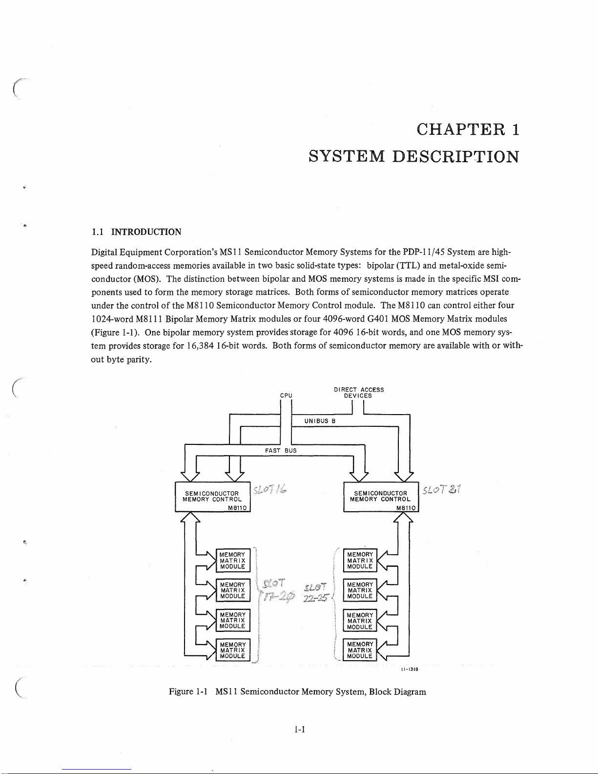
Digital Equipment Corporation's MSl1 Semiconductor Memory Systems for the PDP-I 1/45 System are highspeed random-access memories available in two basic solid-state types: bipolar (TTL) and metal-oxide semiconductor (MOS). The distinction between bipolar and
ponents used to form the memory storage matrices. Both forms
under the control
of
the
M8lI
0 Semiconductor Memory Control module. The
1024-word M8111 Bipolar Memory Matrix modules or four 4096-word
(Figure 1-1). One bipolar memory system provides storage for 4096 16-bit words, and one
tem provides storage for 16,384 16-bit words. Both forms
out
byte parity.
CPU
MOS
memory systems
of
semiconductor memory matrices operate
of
semiconductor memory are available with
DIRECT
ACCESS
DEVICES
UNIBUS
B
G40l
is
made
in
M811
0 can control either four
MOS
Memory Matrix modules
the specific
MOS
memory
MSI
or
com-
sys-
with-
(
SEM I CONDUCTOR
MEMORY
Figure
1-1
FAST BUS
CONTROL
Me110
MS
11
Semiconductor Memory System, Block Diagram
1-1
11-1316
The bipolar and
MOS
semiconductor memories can be jointly or separately operated from either the
KB
11
Fastbus or the PDP-II Unibus, or from both, depending on the specific PDP-l 1/45 System configuration. When
operated from the Unibus, each semiconductor memory system functions
and can serve
as
the basic memory in a large-scale system. Operation under joint control
Unibus provides direct high-speed memory access through the Fastbus for the
ing the processor/peripheral relationships characteristic
of
the Unibus. Whether operating jointly or separately
with the Unibus and/or Fastbus, a semiconductor memory always assumes the role
processor. Under Unibus control, the memory also
designated
"master".
is
"slave" to any peripheral (direct access) device currently
as
a PDP-II compatible peripheral
of
the Fastbus and
KB
11
Processor, while maintain-
of
a "slave" device
to
the
Because readout from semiconductor memories
ferrite-core memories
tically much faster than
of
bipolar memory
is
eliminated. In addition, the switching speed for semiconductor memories
that
for
the
ferrite-core memory. The extremely high switching speeds characteristic
cells
permit memory cycle times
semiconductor memory systems have slower cycle times
1.2
M8111 BIPOLAR MEMORY
MATRIX
The M8111 Bipolar Memory Matrix module
either store or not store byte parity. The M811I
TTL
MSI
memory circuits, interconnected to form a 1024 X IS-bit memory matrix. Each IS-bit word in this
matrix
is
formed by two S-bit bytes and two parity bits, one per byte. This module also contains appropriate
address decoding and driving logic,
ing inversion and driving logic
module are jumper-connected so
to decode a unique address. The
respects, except that the
a
1024 X 16-bit memory matrix without byte parity.
1.3 G401
The G401
MOS
MEMORY
MOS
Memory Matrix module
MSl11 contains sixty-four 256 X I-bit
MATRIX
also configured to either store or
two
1024 X I-bit
ration
is
exactly the same
MOS
MSI
as
IS write-data inversion stages, and control-signal decoding logic. All decod-
is
formed by TTL integrated circuits. Address lines
that
in a given bipolar memory system each matrix module can be configured
MS111 Bipolar Memory Matrix module
MODULE
is
not
store byte parity. The G40 1 Y A parity-equipped module contains seventy-
circuits, interconnected to form a 4096 X IS-bit memory. The IS-bit word configu-
the bipolar matrix, i.e., two S-bit bytes and two parity bits, one per byte. This mod-
ule also contains appropriate logic to level-shift addresses, data, and control signals from TTL to
is
non-destructive, the write-after-read-cycle time associated with
of
MODULE
is
an 8-1/2 in
YA
parity-equipped modules contain seventy-two 256 X I-bit
an S-1/2 in. X
300
ns
for an operating bipolar memory system.
of
450 ns.
.. X 15
in. multilayer glass hex board, configured to
<14:
II>
is
identical to the M8111 Y A in all
MSI
memory circuits, interconnected to form
15
in. double-sided, multilayer
at each
MSlll
glass
hex circuit board;
MOS
to TTL voltage levels; and 16 or IS intergrated-circuit sense amplifiers, depending on whether parity
one for each
decoded at this module to select the specific module and the group
module. Addtess bits
wired for a unique address assignment. The
G40l Y
a
4096 X 16-bit memory matrix without byte parity.
of
the read-sense lines. The states
MAD
<I
4:
13)
are jumper-connected
A,
except that the G401 contains sixty-four 1024 X I-bit
of
memory address (MAD) register bits (02:01) and
G401
MOS
Memory Matrix module
of
1024 words addressed within the selected
so
that
each 4096-word matrix can be selected and
is
identical in all respects to the
MSI
memory circuits, interconnected
is
characteris-
MOS
and
is
specified,
<14:
13) are
to
matrix
MOS
form
of
the
MOS
Operation
because
of
the nature
memory matrix
of
the dynamicMOS storage cell (Appendix A), each memory access must include a time
interval for pre charging the addressed cells prior
system must be periodically refreshed, usually every 1
intervals.
is
substantially different from
to
the actual access. Second, all memory locations in an
ms,
to assure data validity during any extended standby
1-2
the
bipolar matrix in two respects. First,
MOS
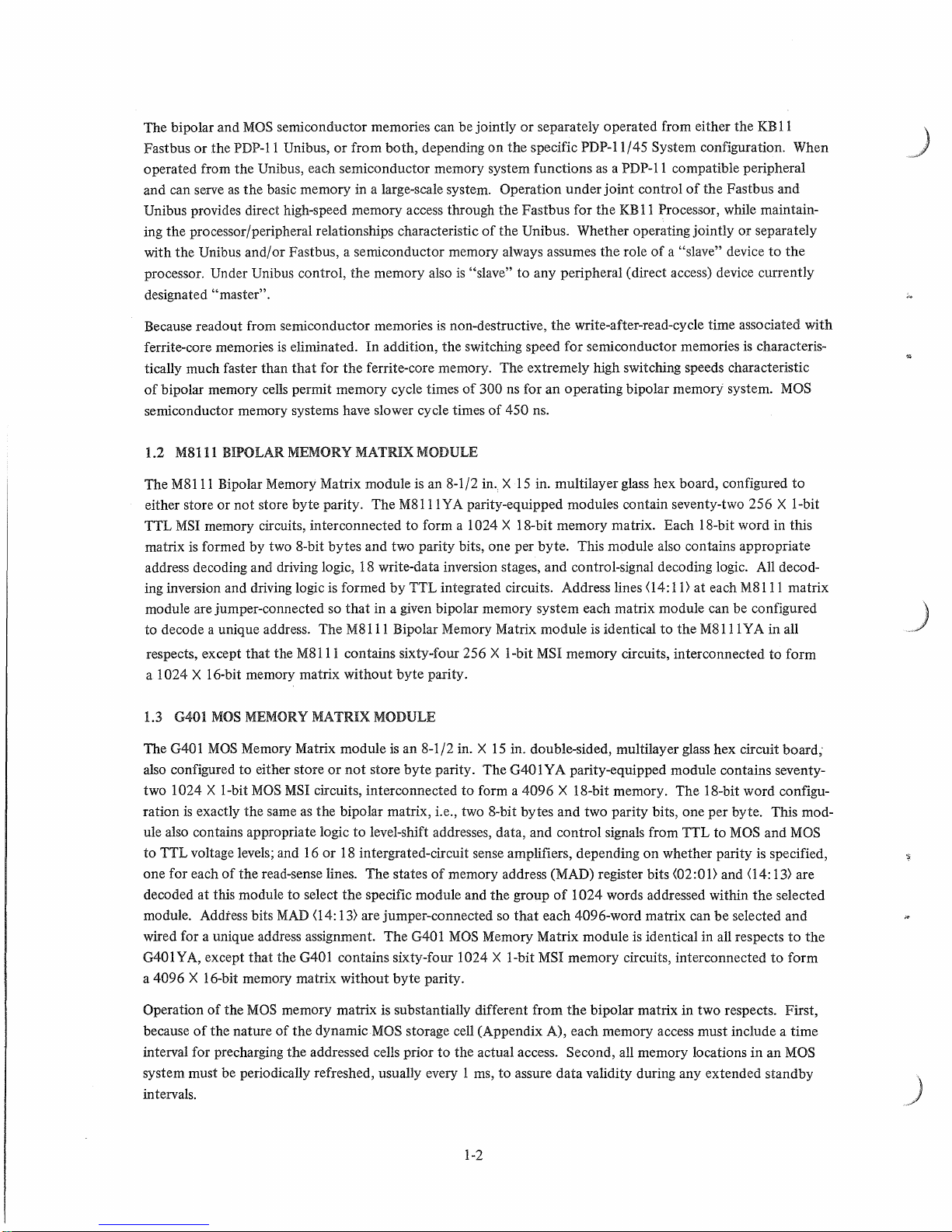
1.4 M8110 SEMICONDUCTOR MEMORY CONTROL MODULE
The
M811
0 Semiconductor Memory Control module
of
controlling either four
trol
is
shown in Figure 1-2. The
tween the PDP-l 1/45 Fastbus and a Unibus, and directs logic and timing sequences necessary for the storage
retrieval
described briefly in the following paragraphs.
of
each data word
r
~'~M;O;;
M81ll
or four G40l matrix modules. A simplified block diagram
M8ll0
or
byte associated with a given access cycle. Each
control multiplexes memory access addresses and associated data
C-;T;L------- - _
is
a fully integrated two-port memory controller capable
of
the
of
the
M8ll
0 control functions
FAST
BUS
.......
~:~~
-----,
M8ll
0 con-
be-
or
is
I
I
I
REFRESH
(MOS MEMORY ONLY) MULTIPLEXER
LOG
IC
,....-------+\
TIMING
AND I
CONTROL
1--
_____
MEMORY
ADDRESS
---.
/.;111.,.,;1;....-._-,
~
I I
I I
I
DIAGNOsl~g
i PARITY
L
_______
LOGIC
CONTROL
I-----t- DATA
REGISTERS",
~~--
(A
r----I-
~v
16K
4K
BIPOLAR
MOS
MEMORY
OR
I
i
_J
'-/
MEMORY
v
UNIBUS B
Figure
1-2
MSll
Semiconductor Memory Control Module, Block Diagram
1.4.1 Memory Address Multiplexing
The memory address multiplexing function involves two sequential actions under direct control
timing and control logic. First, based on priority, arbitration
ing and control logic, Fastbus, Unibus, or refresh addresses (for
the memory address (MAD) register. Second, through a parallel bit-to-bit connection scheme, Fastbus or Unibus
addresses are mapped into the
associated bipolar
and control function.
or
MOS
MAD
register. Once mapped into the
memory matrix module selected by
of
memory access requests performed
MOS
memory systems only) are multiplexed into
MAD
register, and address
that
address through action
of
is
strobed into the
of
the
M811
the
by
y
11-1317
M811
0
the tim-
0 timing
1.4.2 Write and Read Data Registers
The M8110 contains two data registers: the write-data (DATO) register, and the read-data (DATI) register. The
DATO register multiplexes a 16-bit data word (or two 8-bit data bytes), from either the Fastbus
stores
that
data until strobed into the associated bipolar or
18-bit
DATO register stores parity for the lower and upper data bytes in the most significant DATO register
stages. These parity bits are generated
as
MOS
memory matrix module
part
of
word or byte storage in the DATO register. Data from the
1-3
by
or
Unibus, and
the M811
O.
The
Unibus is received
is
received directly
appropriate time,
at
the
M811 a Unibus interface for storage in
at
the
DATO register because
the
data accompanying a DATO cycle is strobed
associated address.
The
M8110 DATI register receives and stores
result
of
a Unibus
Unibus interface,
Unibus
data
or
Fastbus DATI cycle.
and
to
the
Fastbus for retrieval
lines are bidirectional.
At
data
the
the
of
the
proximity
from
the
location addressed
end
of
a DATI cycle, data is
by
the
requesting bus. Fastbus
DATO register. Fastbus
of
the
into
M811 0
the
to
memory
in
the
strobed
data
the
KB
location designated
memory
jointly
lines are unidirectional,
data
11
Processor.
matrix
onto
to
be written
as
the
M8110
At
the
by
the
a direct
1.4.3 Timing
The
M811 0 timing
multiplexing priorities, timing,
In addition, specific portions
to
identify
tions
or
are
to
be interleaved.
strobe levels necessary
nent
registers.
the
DATO operation.
Because
dressed
operation receives
and
Control
and
control interprets
the
physical memory selected,
one
out
of
four 4096-word sections),
If
the
to
The
timing and control logic also enables
readout
data
from semiconductor memories is non-destructive,
onto
the
output
the
data
and
the
nature
of
the
address contained
operation
to
load multiplex addresses
lines which connect
at
the
bus
input
1.4.4 Refresh Logic
The nature
storage cell, which is
the
data stored. Refreshing
row address for
by
generating 32 sequential row addresses during
the
address multiplexer. Coincident control levels
tion
of
the
of
the
that
timing
dynamic
the
circuit equivalent
circuit
and
control logic
MOS
MSI circuits forming
the
data contained in each integrated-circuit memory requires
be
cycled each 1 ms.
to
permit
control
of
signals
the
operation
in
the
memory
the
required
be
performed
and
to
both
as
the
data
the
of
a capacitive node,
The
M811 0 refresh logic performs this function automatically
each
I-ms period. These sequential addresses are
from
the
input
of
refresh addresses
from
the
Fastbus
to
be
the
MAD register are decoded
section
to
be
byte
configuration,
is a DATO,
data, according
the
designated memory section for writing
buses. In this case,
or
subsequently
addressed
the
timing
to
the
the
timing
Unibus and derives
performed
(one
out
and
to
determine
and
control
priority
and
the
of
control
bus
that
requested.
G40 1
MOS
Memory Matrix module requires
be
periodically charged above
refresh logic serve
at
the
to
enable
assigned
priority
the
internal
(DATO
by
the
selection logic
of
four
l024-word
if
data
logic develops
the
request,
into
and
logic strobes
initiated
that
the
the
threshold
all states
then
the
address priority por-
level.
or
DATI).
words
the
perti-
performs
the
read
that
each
of
the
input
sec-
ad-
of
to
Each DATO
cludes
or
the
pre charging
DATI operation
or
refreshing
memory matrix modules, this refresh logic is
1.4.5 Parity
Data
to
erated
DATOB, parity is generated
During DATI operations, parity
data register.
Control
be written is transferred
and
stored
in
bit
16 for
If
a parity error
the
only
is
is
(with
the
exception
of
each address written
to
the
M81l
low-order
for
checked
detected,
the
byte
byte
after
the
of
inhibited
0 over 16
and
written
each
16 bits
respondent
the
write
into
and
the
precharge interval
data
lines.
in
bit
17 for
and
stored in
of
bus is notified.
1-4
portion
or
data
of
a write-after-read operation) also in-
read. When
If
the
operation is a DATO cycle, parity is gen-
the
high-order
the
corresponding
read are transferred
the
is
byte.
M81!
0 is used with bipolar
ignored.
If
the
operation
parity.
to
the
M81l 0 output
is
a
1.4.6 Diagnostic Logic
(
M8ll0
even in any memory address, and
ated.
jumper-connected
Each
control signals
loaded is
In
while protecting those memory areas occupied
ter
is
1.5
Storage Capacity
Maximum Access Time:
Maximum Cycle Time
Operating Voltages:
memory control diagnostic logic allows writing
to
check
the
parity generated for
Part
of
the
M8110 memory control diagnostic logic structure decodes specific Unibus addre'Sses
at
each
M8l1
0 so
that
each
half
control also contains two diagnostic parity registers
to
select
one
of
these two registers for loading
then
interpreted
this manner, diagnostic software can selectively exercise designated semiconductor
can also be selectively read through execution
transmitted directly
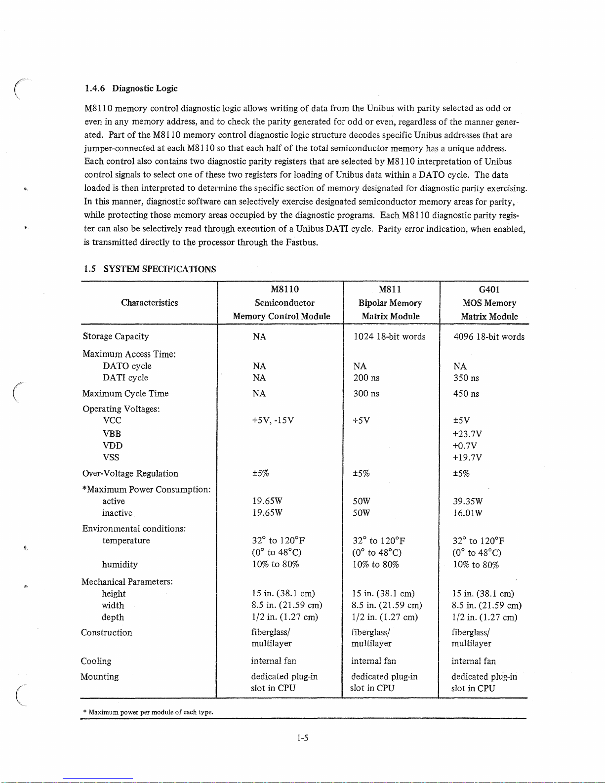
SYSTEM SPECIFICATIONS
Characteristics
DATO cycle
DATI cycle
VCC
to
to
determine
the
processor
the
specific section
by
through
Semiconductor Bipolar Memory
Memory
Control
NA
NA NA
NA
NA
+5V, -15V
of
data from
of
the
total
that
of
the
diagnostic programs. Each
of
a Unibus DATI cycle. Parity error indication, when enabled,
the
Pastbus.
M8110
Module Matrix Module
the
Unibus with parity selected
odd
or
even, regardless
semiconductor
are selected
of
Unibus data within a DATO cycle. The data
memory designated for diagnostic parity exercising.
by
M811
1024 I8-bit words
200
ns
300
ns
+5V ±5V
VBB
VDD
VSS
Over-Voltage Regulation
*Maximum Power Consumption:
active
inactive
Environmental conditions:
temperature
humidity
±5%
19.65W
19.65W
32°
to
(0°
to
10%
to
0
120
48°C)
80%
±5%
50W
50W 16.01W
p
32°
(0°
10%
to
to
to
120
48°C)
80%
of
the
manner gener-
memory
M81! 0 interpretation
has a unique address.
memory
M8ll
0 diagnostic parity regis-
+23.7V
+0.7V
+19.7V
0
p
32°
(0°
areas for parity,
MOS
Matrix Module
4096
NA
350 ns
450
±5%
39.35W
10%
as
odd
that
of
Unibus
G401
Memory
18-bit words
ns
0
to
120
p
to
48°C)
to 80%
or
are
Mechanical Parameters:
height
width
depth
Construction
Co
0
li.l1g
Mounting
(
* Maximum power per module
of
each type.
15 in. (38.1 cm)
8.5 in. (21.59 cm)
1/2 in. (1.27 cm) 1/2 in. (1.27 cm)
fiberglass/
multilayer multilayer multilayer
internal
dedicated plug-in
slot in
fan
CPU slot in CPU
1-5
15
in. (38.1 cm)
8.5 in. (21.59 cm)
fiberglass/
internal
dedicated plug-in
fan
15
in. (38.1 cm)
8.5 in. (21.59 cm)
1/2 in. (1.27 cm)
fiberg1ass/
internal
dedicated plug-in
slot in CPU
fan
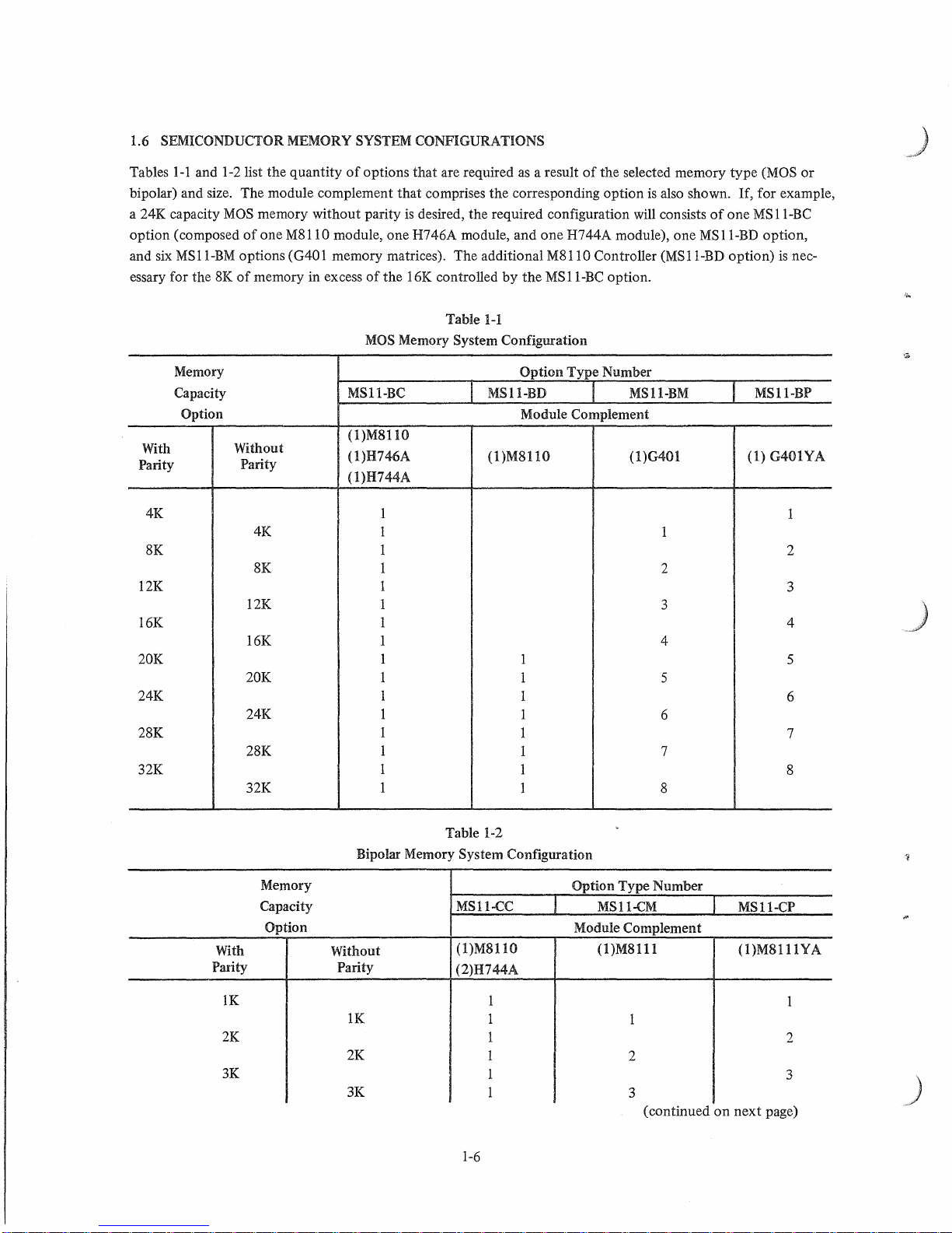
1.6 SEMICONDUCTOR MEMORY SYSTEM CONFIGURATIONS
Tables
1-1
and
1-2
list the quantity
bipolar) and size. The module complement
a 24K capacity
option (composed
MS
and six
essary for the 8K
MaS
memory without parity
of
one M8110 module, one H746A module, and
Il-BM options (G40 1 memory matrices). The additional
of
memory in excess
of
options
that
that
is
of
the 16K controlled
MOS
Memory System Configuration
are required
as
comprises the corresponding option
desired, the required configuration will consists
by
the
1-1
Table
a result
of
the selected memory type
is
also shown.
of
one
one
H744A module), one MSII-BD option,
M8II
MS
II-Be
0 Controller
option.
(MS
II-BD option)
(MaS
If,
for example,
MS
II-BC
is
or
nec-
Memory
Capacity MSII-BC
MSl1-BD MSII-BM
Option
(l)M8110
With
Parity
4K
Without
Parity
4K
(l)H746A
(1)H744A
I
1
(l)M8110
8K 1
8K
12K
1
I
12K 1
16K
16K
1
1 4
20K 1 1
20K I
24K 1
24K
28K
28K
32K
32K
I
1
1
I
1
Option
Type
Number
Module Complement
(1)G401 (1) G401YA
1 5
1
1
1
1
I
1 8
MSII-BP
1
1
2
2
3
3
4
5
6
6
7
7
8
Memory
Capacity MSII-CC
Option
With
Parity
lK
2K
3K
Bipolar Memory
Without
Parity
IK
2K
3K
Table 1-2
System Configuration
(l)M8110
(2)H744A
I
1
1
1
1
1
1-6
Option Type Number
MSII-CM
Module Complement
(1)M8111
1
2
3
(continued
MSII-CP
(l)M8111YA
on
next
1
2
3
page)
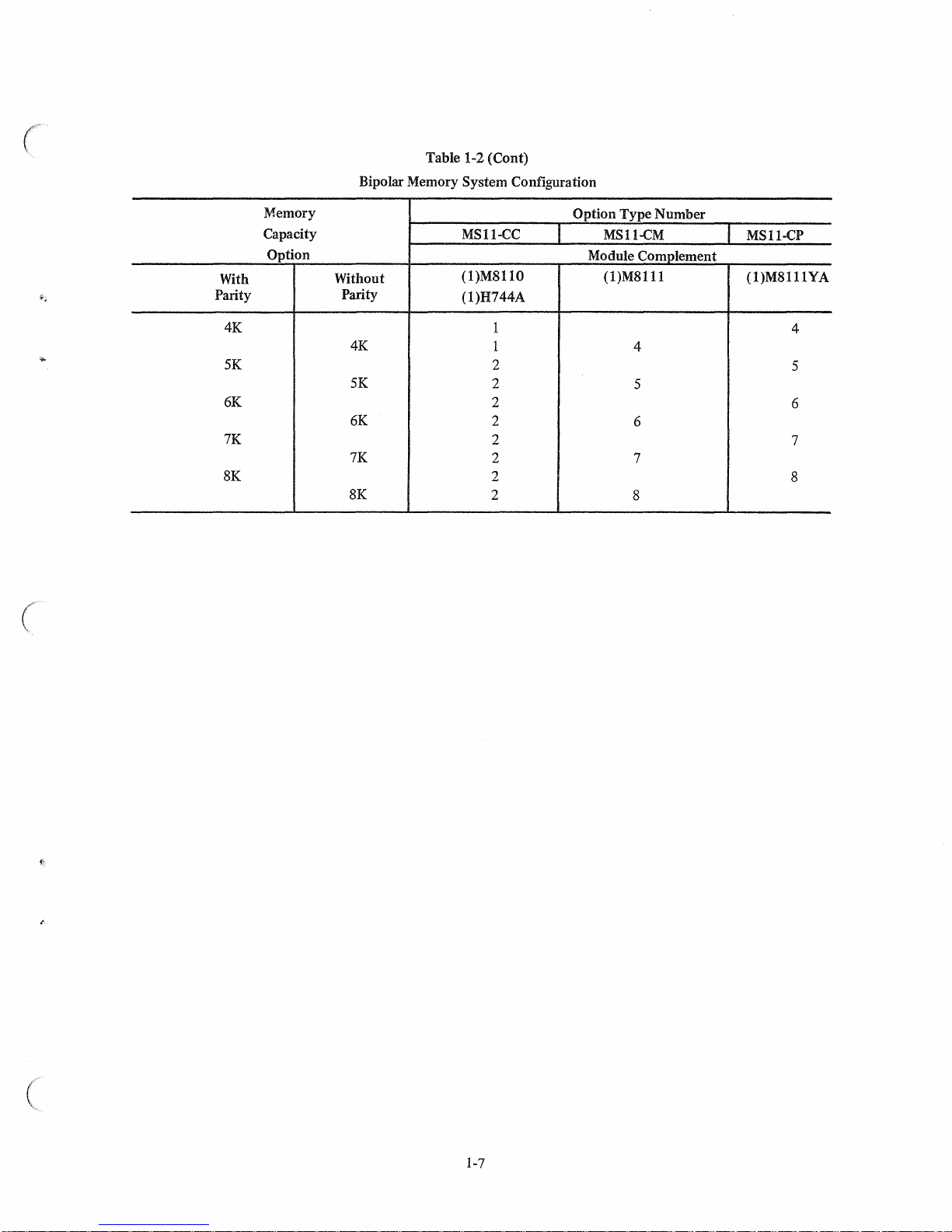
Table 1-2 (Cont)
Bipolar Memory
System Configuration
Memory
Capacity
Option
With
Parity
4K
5K
6K
7K
8K 2
Without
Parity
4K
5K
6K
7K
8K
MSII-CC
(1)M8110
(1)H744A
Option
Type
Number
MSII-CM
Module Complement
(1)M8111
1
1
2
2
2
2
2
2
2
4
5
6
7
8
MSII-CP
(1)M8111YA
4
5
6
7
8
(
1-7

CHAPTER
2
MEMORY
INTERFACE
2.1 INTRODUCTION
A PDP-I 1/45 System can be equipped with one
MSIIO module, in turn, can exercise control
G401
MOS
Memory Matrix modules. Since the memory capacity
(the
MSlll
mined by the selected configuration. A typical
polar memory in IK increments
might also have one
However, memory matrices
Tables
configuration
bus, and processor relationship. Within a
semiconductor memory controls through an extremely high-speed information
and under control
the two
provides
1-1
and 1-2, the memory capacity determines the number
MS11
IK
and the G401 4K
or
up
to
of
the controllers directing bipolar matrices while the
of
different types can
is
4K
of
bipolar
of
the CPU Fastbus. One Unibus in
0 controls.
or
16K
of
or
two MSIIO Semiconductor Memory Control modules. Each
of
up
to four
MSIII
of
memory) the total memory capacity available
two-MSll
32K
of
MOS
not
MOS
memory per module). Figure
PDP-l 1/45 computer system, the CPU communicates with associated
0 module arrangement can consist
memory in 4K increments. The two-controller configuration
be connected to the same
the
system, normally Unibus
Bipolar Memory Matrix modules,
of
these two matrix module types
other
of
MSII
0 modules required
2-1
SYSTEM
OPERATIONS
or
up
to
is
different
to
the user
of
up
is
connected to
MSll
0 control.
(the
illustrates the memory system,
path
which
is
internal to the CPU
A,
also communicates with
to
SK
MOS
matrices.
As
indicated in
maximum
is
deter-
of
four
bi-
(,
MSll
Each
fore, an operating
Unibus interface, and the memory bus. The relationship
to these interfaces
are physically located in
matrix module connectors
second
and receive information and control signals
connection between an
physically adjacent connectors, so
Discussion
definition
used
2.2
MS
11
pause for a write following a read. These operations are designated
0 control, in turn, communicates with up
MSII
0 Semiconductor Memory Control has three active interfaces: the Fastbus interface,
is
shown
in
Figure 2-2. Because the
the
PDP-l 1/45 processor, connection to the Fastbus
to
the
PDP-I 1/45 CPU backplane. However,
Unibus, with respect
of
semiconductor memory system interfaces will involve a description
of
each interface
to
address semiconductor memories.
BASIC MEMORY ACCESS OPERATIONS
Serr>Jconductor M:emory Systems operate in four accessing modes: read, write, optional
to
the
MSII
0 control, requires a defined Unibus interface on the control
to
MSII
0 control and associated MSl11 bipolar
that
control-matrix module information and signals are direct-wire connected.
in
terms
of
information and signals exchanged, and an explanation
to
and from
four bipolar or four
of
a typical PDP-l 1/45 Semiconductor Memory System
MSII
0 control and associated memory matrix modules
that
Unibus. Like the Fastbus connection, memory bus
as
MOS
is
the
potentially remote location
or
G40 I
MOS
follows:
memory matrix modules. There-
by
direct-wiring the control and
of
a
to
drive
memory modules involves
of
memory access operation, a
of
the conventions
byte
handling, and
the
2-1
Each
of
(UNIBUSAI
AND
UNIBUS
NORMALLY
CONNECTED) I
a.
Read Data (DATI)
b.
Read data and pause (DATIP)
c.
Write data (DATO)
d.
Write data bytes (DATOB)
these modes are briefly discussed in the following paragraphs.
UNIBUS
A
I
I
I
I
I
I
PDP-11/45
CPU
I
I
I
B
I
I I
I I
I I
I I
I I
4K
BI-POLAR
OR
16K
MOS
4K
BI-POLAR
OR
16K
MOS
I I
I I
I
UNI BUS B
Figure
2-1
Semiconductor Memory Configuration within
In
2.2.1 Data
During a DATI cycle, data in the locations addressed
put
data latch for retrieval by the initiating bus (Unibus
destructive; thus, the restore portion
2.2.2 Data In,
The purpose
that
til
ways followed by execution
cept for a pause for initiation
(DATI) Cycle
at
the memory matrix module is loaded into the
or
Fastbus). Readout
of
the conventional core memory read cycle
Pause (DATIP) Cycle
of
this reading mode
is
to
hold memory secure after data is read from a set
data can be revised and then written again. PDP-II convention requires
of
a DATO
of
the impending DATO or DATOB.
or
DATOB operation. A DATIP is a duplicate
PDP-ll/45
of
that
Systems
semiconductor memories
is
not
required.
of
memory addresses un-
execution
of
of
a DATI operation ex-
11-0833
M8ll0
a DATIP
is
is
out-
non-
al-
2-2
MBlll
BI-POLAR
OR
G40l
MOS
MEMORY
MATR
IX
MODULE
~------------------------------------~
MBlll
BI-POLAR
OR
G40l
MOS
MEMORY
MATRIX
MODULE
M8ll0
M8lll
BI-POLAR
OR
G40l
MOS
MEMORY
MATR
MODULE
MEMORY
BUS
~------------------------------------~
M8ll0*
M8ll1
BI-POL.A.R
OR
G40l
MOS
MEMORY
IX
MATRIX
MODULE
FAST
FAST
BUS
BUS
INTERFACE
INTERFACE
SEMICONDUCTOR
MEMORY
CONTROL
M8ll0*
SEM I CONDUCTOR
MEMORY
CONTROL
M8ll0
MEMORY BUS
UNIBUS
INTERFACE
UNIBUS INTERFACE
M8lll
BI-POLAR
OR
G40l
MOS
MEMORY
MATRIX
MODULE
* A SINGLE
FOUR
MODULE TYPES.
M8llO
M8lll
CAN
MODULES BUT NOT A
DIRECT EITHER FOUR
Figure
(
M8lll
BI-POLAR
OR
G40l
MOS
MEMORY
MATRIX
MODULE
G40l
MIXTURE
2-2
MODULES
OF
THE TWO
Semiconductor Memory System Interfaces
OR
M8lll
BI-POLAR
OR
G40l
MOS
MEMORY
MATRIX
MODULE
2-3
M8ll1
BI-POLAR
OR
G401
MOS
MEMORY
MATRIX
MODULE
11-0826
2.2.3 Data Out (DATO) Operation
A DATa, or write operation, causes data outgoing from the Unibus
(16 bits) at the address order designated. The nature
written in do not require prior clearing.
As
a consequence, the writing
of
semiconductor memories
or
Fastbus to be written one word at a time
is
such
that
locations to be
of
data begins immediately after cycle in-
itiation, with no prior clearing required.
2.2.4 Data
A
DATOB
word. Decoding
bus
is
to be written in memory
Out, Byte (DATOS) Cycle
cycle
is
a duplicate
of
each address designates whether
to be written
as
a low-
of a DATa
or
high-order byte in the 16 bits available at each memory location. Therefore, data
as
bytes must be received
cycle, except
the
on
that
data
is
written
as
8-bit bytes rather than
corresponding byte transferred from the Unibus or Fast-
the data lines corresponding to the byte position designated
as
a l6-bit
by the address.
2.3 F
ASTBUS INTERFACE
The Fastbus interface provides a high-speed, full-duplexed, dedicated data path between the processor and the
M8110 Semiconductor Memory Control. The Fastbus address, data, and control1ines are defined in Table
Table
2-1
2-1.
Fastbus/M8110 Interface and Control Signals
Name
Address
Data In
Data
Out
Bus
Start
Memory SMCFMEM L SMCF
Selected
Control OK
Memory
Control UBCC
Control
Bus End
Clear
Parity Error
Halt
Parity Error
Flag
Parity Error
Acknowledge
Sync
Mnemonic
DAPB BAMX (05:00) H
SAPJ PA
SCME
PDRB
TMCE BUS OUT L TMCE
UBCA CONTROL OK H UBCA
SMCA MEM SYNC (B) L SMCA TIGA
UBCC MEM BUS CI L UBCC
TMCE BEND CLR L TMCE
SMCB
SMCB
UBCB
07:06)
MEM
D (15:00) H
BR
05:00)
MEM
BUS
PE HALT L
PERF
L
PERF
ACKN L
H
CO
B L
L
Source Destination
Drawing
DAPB SMCC selects
SAPJ
SCME
PDRB
UBCC
SMCB
SCMB
UBCB
Drawing
PDRA
SMCD DATO
SMCA starts Fastbus-initiated
TMCF informs Fastbus
SMCA informs control
SMCA specifies type
SMCA
SMCA terminates current
UBCB
UBCB
SMCB
DATI lines from
cycle
conductor
cycle can be completed
informs Fastbus
access cycle
(Table 2-2)
specifies type
(Table 2-2)
cycle
ticipated address
initiates processor
error
sets processor parity
acknowledgment
receipt
memory
lines from
memory
is
at
M811 0
of
parity
Function
location
Fastbus
Fastbus
that
that
current
that
being
completed
of
memory
of
memory
memory
control
is
incorrect
HALT
error
by
processor
error
memory
address
access
current
access cycle
access cycle
access
if
Fastbus an-
on
parity
flag
indication
access
is
in semi-
memory
of
2-4
2.3.1
Fastbus
Initiation
memory address on
at
the
same time. The address bits are decoded in
processor denotes receipt
that
controller having this address within its assigned range
Processor response
from
also
memory
The
Required timing signals are also furnished
OK,
are
from
these
ory access cycle. Since this is a request
the
timing operation), together
functions;
DATA
LATCH. The final steps are accomplished with DATA LATCH;
latched
location with
into
DATO Cycle
of
a semiconductor
the
to
MEM
the
processor, asserts PREQ (1) H. This
now
two
it
is returned
the
address
decoded
is
to
control bits. With
Data
In
the
concurrent WRITE PULSE.
memory
address lines (Figure 2-3). Data
of
a valid address. Although
is
TMCF FAST L, which inhibits Unibus
now' latched
indicate a
to
Fastbus
Register, placed
into
DATa
the
with
CONTROL
to
access cycle via
the
memory selection logic and
latter
the
MAD register and a usable address
to
the
memory logic.
operation. Table 2-2 lists
subsequent CONTROL OK signal,
from
the
processor (PREQ), ACCESS READY LATCH H (a
OK, generates
inform
on
the
Fastbus
the
processor
bus
to
Table 2-2
and
Unibus Control Bit States
the
Fastbus occurs when
to
be stored
the
address is transmitted
of
signal, together
that
the
memory module, and
at
this address
addresses will acknowledge with
memory
with
MEM H, initiates memory timing.
MEM
BUS
CO
the
four access cycle types
the
processor verifies
MEM
SYNC. This latter signal performs several
data
is
to
be
stored and, with
the
data
the
processor places
is
present
the
resultant
to
both
M811 0 controls, only
addressing. TMCE BUST OUT L,
is
presented
and
Cl,
to
be written (Data
then
to
received prior
stored
at
the
desired
on
the
DATa
MEM
signal
the
MEM
the
memory module.
to
CONTROL
that
are decoded
the
current mem-
product
MEM. C 1,
the
develops
Out)
specified
lines
to
signal.
of
is
the
Input
Fastbus
UBCCMEM
C1L
Usable
SMCA SMCA
MEMCIL
0
0
1
1
The
KB
11
Processor, during execution
next
ed
bus cycle
requires data,
aimed
to
the
cycle initiated
for purposes
to
fetch
at
retrieving
the
semiconductor memory control.
discontinued bus cycle
of
increased operating efficiency. After each instruction fetch,
the
word following
not
from
the
the
next
by
TMCE BUST OUT L.
from
UBCCMEM
COL
Signal
MEMCOL
0
I
0
1
of a current
the
current instruction cycle.
next
word,
but
from a different address,
word. This terminating process results
At
the
by
responding
with
BUSB
UBCI
instruction,
control
SMCF
SMCH
0
0
1
1
that
MEM
Input
from
Unibus
Cl
L
Usable
H, L UBCOH, L
previously acknowledged
L, TMCE BEND
Signal
attempts
If
then
in
BUSB
CO
SMCH
0
I
0
1
to
predict
the
instruction currently being executed
the
processor terminates
the
processor issuing TMCE BEN CLR L
CLR
L
the
address
the
processor initiates
the
address associated
L terminates
Access
Cycle
to
be
Performed
DATI
DATIP
DATa
DATOB
of
the
that
the
memory access
word need-
another
bus cycle
with
(
2-5
DATO
DATA
CONTROL
MEM
OUT
CI
SYNC
....
DATA
IN
LATCH
REGISTER
I
DATA
-
DATI
CPU
CONTROL
CONTROL Cl
BUST
OUT
MEM
ADDRESS
DATA
OK
MEM SYNC 1
I
(B)
PREQ
T
IN4-----------------------------------------------------~
MEMORY
SELECTION
--------1
I
.---L.-
MEMORY
TIMING
ACCESS
LATCH
READY
MAD
LATCH
REG
SA
LATCH
DATA
REGISTER
WRITE
PULSE
MAD
REGISTER
OUT
r----e--
-'
MEMORY
>-
MODULE
MEM
SYNC4--------L--------------~~----------------------------------~
CPU
CONTROLOK----------------------------------------------------~
BUSTOUT----------------~
MEM
---------------~
ADDRESS
MEMORY
SELECTION
~--------------------------------------------~~
PREQ
(B)
Figure
MEMORY
TIMING
2-3
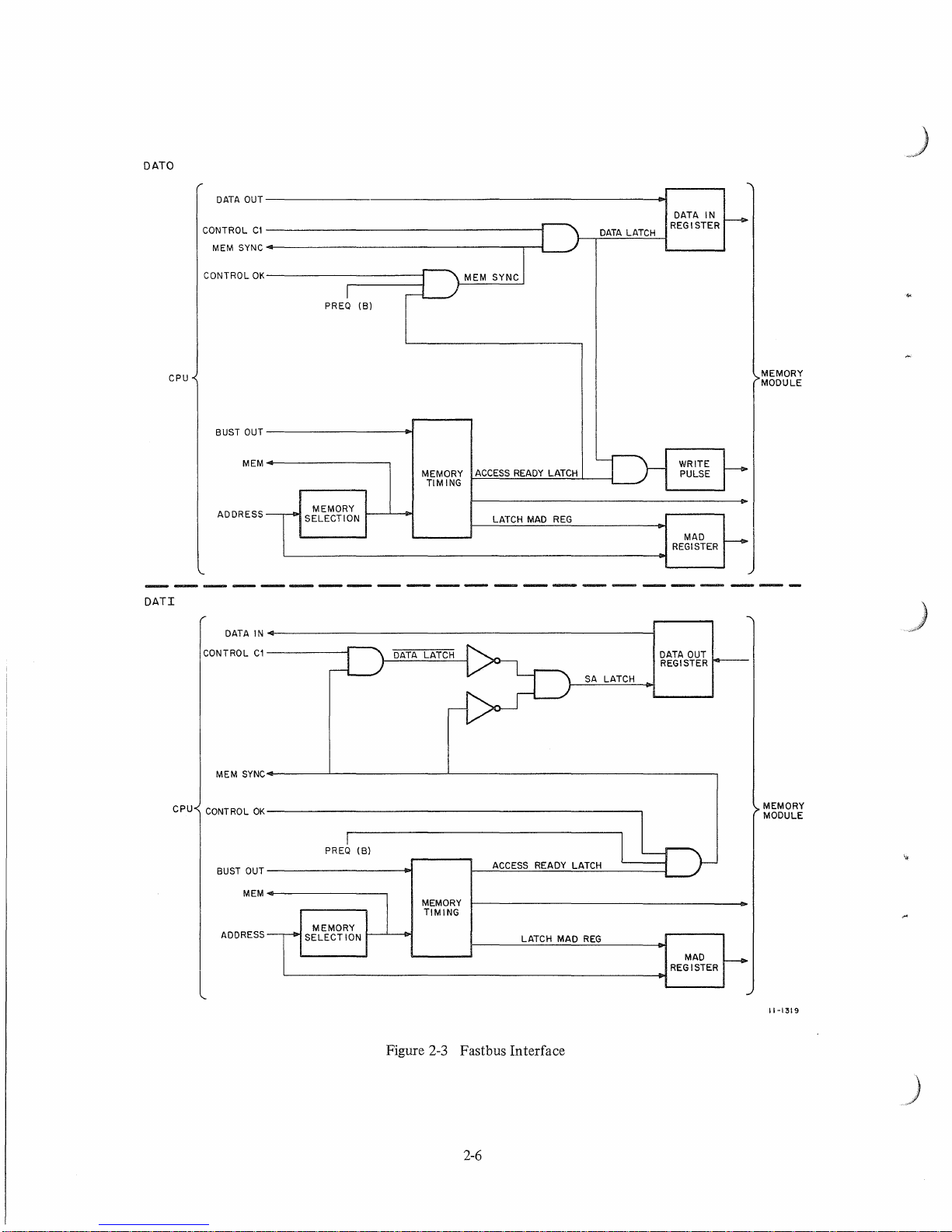
Fastbus Interface
2-6
ACCESS
READY LATCH
LATCH MAD
REG
MAD
REGISTER
MEMORY
MODULE
11-1319
2.3.2 Fastbus DATI Cycle
If
the Fastbus-initiated access cycle
DATO
was
executed. When the memory address from the Fastbus
The
BUST OUT signal from the processor that follows asserts PREQ
H,
initiates memory timing, the memory address
OK
is
received, the timing sequence continues without further processor interruption. ACCESS READY LATCH,
a product
(Table 2-2)
is
set at
then transmitted,
of
the timing process, generates the
is
a 0 for DATI and DATA LATCH
the
termination
of
the
as
DATA IN, from the Data Out Register via Fastbus to the processor.
is
a DATI
MEM
SYNC pulse. The data from the desired address in the memory
or
DATIP (Figure 2-3), the sequence
is
decoded,
(1)
H.
is
placed on the lines to the memory module. After CONTROL
MEM
SYNC signal. Unlike the DATO operation,
is
inhibited. However, due to the signal levels used, SA LATCH
is
essentially the same
MEM
is
This latter signal, together with
returned to
MEM
the
as
processor.
BUS
matrix
when
MEM
CI
is
Although the two
error indicators
cator causes the processor to issue
2.4
UNIBUS INTERFACE
Data transfers through the Unibus between the semiconductor memory system and the processor (or other
vices) are conducted
PDP-ll Unibus Interface Manual). Unlike the Fastbus interface, data lines between the Unibus and
control are bidirectional. The information and control signals passed between the Unibus and the
conductor Memory Control module are defined in Table 2-3.
Name Mnemonic
Address
Data
SYNC
Master
Slave SYNC
Control
Control
Power Low
de
(Bus A)
dcPower
(Bus
Low
B)
M811
0 parity diagnostic registers are addressed and loaded through the Unibus interface, parity
PE HALT and PERF are relayed to
PARITY ERROR ACK to the pertinent M811 0 control.
on
a master/slave basis with the memory in all circumstances having slave status (refer to the
Unibus/M8110 Interface Information and Control
BUSB A 07:00)
BUSB
D
<I
BUSB
MSYNC
BUSB
SSYNC L SMCF
BUSB
CO
BUSB
CI L
BUSADCLO L
BUSB
DCLOL
5:00) L
L
L
L
BUSB
BUSB
BUSB
BUSB
BUSB
BUSA power
control modules
BUSB
control modules
the
processor through the Fastbus. The receipt
Table 2-3
Signals
Source Destination
power
SMCH
SMCH
SMCH
BUSB
SMCH
SMCH
SMCH
SMCH
selects memory location
provides for bidirectional data
transfer between Unibus and
semiconductor memory
initiates memory access cycle
specified by state
andCI
acknowledges connection
specifies type
cycle (Table 2-2)
specifies type
cycle (Table 2-2)
indicates dc voltage
on bus A
indicates dc voltage
on bus B
M8ll
Function
of
of
memory access
of
memory access
of
either indi-
the
M811
0 Semi-
UBCC
out
of
out
of
de-
0 con
CO
tolerance
tolerance
(
2-7
At
the
M8110, all information and control-signal interchange with
on
the
M811 0 control. This logic consists
control-signal transmission
and
receipt
of
a drive/receiver interface designed
from
remote
locations over
the
Unibus is
routed
for
the
Unibus cable module.
through
high-speed
the SMCH]ogic
information
and
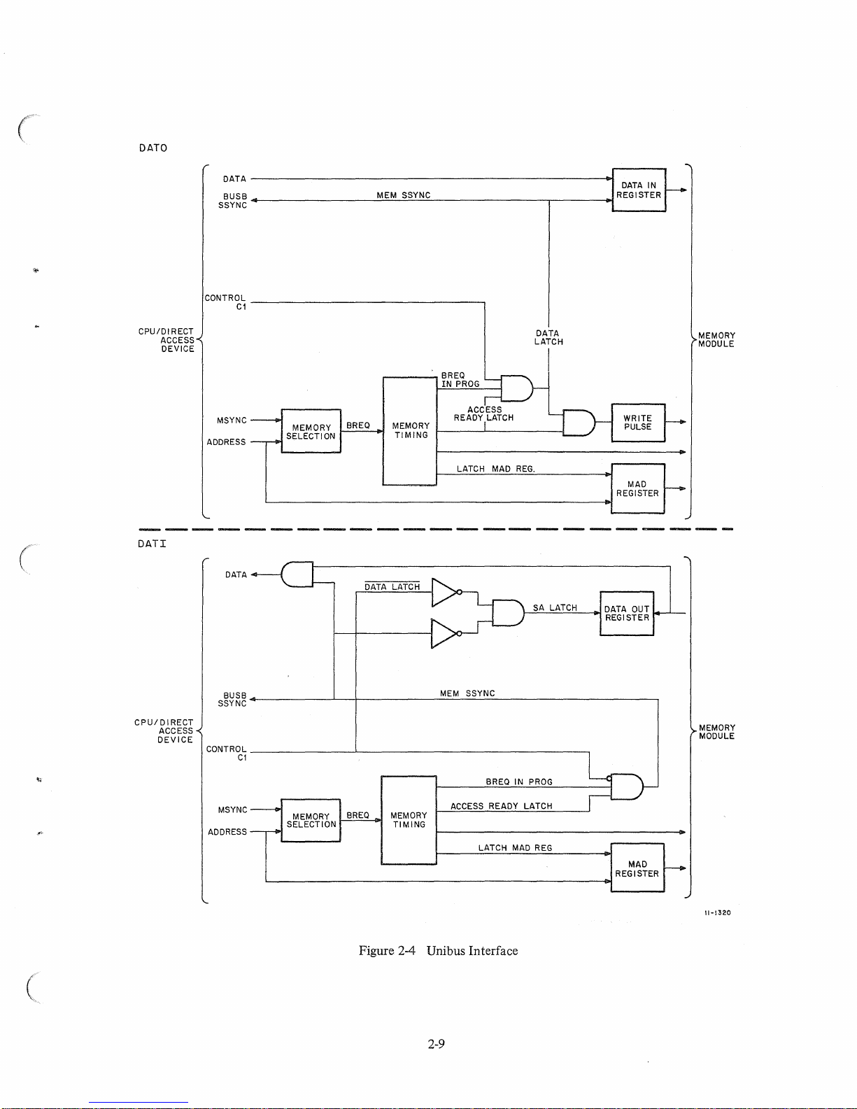
2.4.1 Unibus
A
memory
the
memory
DATO Cycle
access cycle is initiated (Figure 2-4)
add~ess
on
the
input
lines
to
both
from
the
Unibus when
M811 0 controls. Only
the
that
·\the established address range will have its I1!emory selection logic activated.
sent
at
the
control
be
executed.
to
coding circuitry occurs
timing sequence. One
LATCH. Latching
thereby
a delay,
is
stored
bus
which
presented
ACCESS READY LATCH simultaneously produces DATA LATCH
returned,
the
data.
to
the
memory
is
to
access cycle is complete with respect
2.4.2
Unibus DATI Cycle
A DATI memory access operation (Figure 2-4) is similar
access cycle is initiated in
at
the
same time;
the
bidirectional
results in BREQ, which triggers
for
MEM
SSYNC
delivered
by
that
Out
to
ACCESS READY LATCH. MEM SSYNC notifies
the
data requested is available for acceptance. Although SA LATCH
Register en
input
at this time;
The
data
to
with
of
the
of
the
memory address
with
a usable storage address
via
the
Unibus,
DATA
LATCH results.in
matrix.
store
the
data
at
the
CI
is
a
O.
data
lines will
and
the
memory
the
memory matrix along
route
to
the
they
are
decoded
be stored is
the
arrival
concurrently
of
MSYNC from
first signals generated, BREQ
into
the
MAD Register occurs
prior
to
as
BUSB SSYNC, informing
the
DATA
being gated
Concurrent
the
prescribed
M811 0 logic
However, unlike DATO,
be
the
with
this,
memory
to
the
Unibus
on
receipt
used
to
carry
timing sequence
address is
with
latched
required
DATA
location.
and
DATA
the
data
that
into
timing signals.
Unibus.
(Table 2-2)
available
the
IN
the
the
to
on
the
Unibus.
PROG, provides a required condition for DATA
data being
processor
into
LATCH produces
The
advent
M8ll
0 interfacing.
to
the
Unibus DATO
of
the
memory
is
not
sent from
retrieved from
follows. BREQ IN
the
MAD register.
the
processor
determine
DATA lines. Enabling
The
next;
strobed
that
the
address.
memory
MEM
that
the
is
processor
control
Control
subsequent
and
the
Data
the
of
PROG
The
SSYNC
timing sequence
set,
or
direct access device places
where
the
address falls within
bits
CO
and
CI
the
type
of
memory
of
the
BREQ initiates
the
memory
over
the
MEM SSYNC.
selected
In
Register
WRITE PULSE,
matrix
memory
control
and
bus. Following
The
has accepted
then
the
SSYNC disables MSYNC and
procedure
Control
the
processor in a DATI
back
selected
the
described above.
bits
to
the
fulfills
memory
is
brought
read
data
CO
and
processor. MSYNC
the
second
up,
after
is
completed
bypasses
are also pre-
access cycle
address de-
the
memory
module
latter
signal
placed
function
the
Clare
input
operation;
requirement
address is
a delay,
and
the
Data
is
and
on
of
The
then
the
2.5
MEMORY BUS
Figure 2-5 is a simplified block diagram
conductor
the
The
the
from
cases, memory is multiplexed
tion,
the
of
data
Memory
Fastbus, Unibus,
multiplexing
Control
of
module
and
semiconductor
memory access
M811 0 control. This logic arbitrates
the
Unibus
and
Fastbus.
In
between
any
memory
M811 0
on
access cycle, once started, locks
memory
this
bus
portion
is
of
coupled
the
memory
of
and
implements
memory
operations
memory
such
arbitration,
the
to
both
bus is handled
the
semiconductor
system storage.
over
the
access requests
Unibus memory access cycles have higher priority.
Fastbus
and
out
the
Fastbus
memory
the
multiplexing
memory
bus is governed
only
the
Unibus
all
other
bus requests
data-in lines
by
the requesting bus.
2-8
bus. This bus
of
DATO and
by
is
part
DATI
priority
of
the
M811 0 Semi-
operations
arbitration
between
when simultaneous requests are received
on a "first
and
come, first served" basis.
until
completed.
the
Unibus
interface
The
so
that
DATI side
disposition
logic
In
In
all
addi-
on
other
of
'
..
DATO
CPU/DIRECT
ACCESS
DEVICE
DATI
DATA
BUSB
SSYNC
CONTROL
C1
MSYNC
ADDRESS
DATA
MEMORY
SELECTION
BREQ
DATA
MEM
...--
MEMORY
LATCH
SSYNC
__
TIMING
__.BREQ
IN
PROG
ACCESS
READY
LATCH
LATCH
MAD
REG.
DATA
LATCH
I
DATA
IN
REGISTER
MAD
REGISTER
-
MEMORY
MODULE
CPU/DIRECT
ACCESS
DEVICE
S~~~~4-
CONTR~~
MSYNC
ADDRESS
__________
________________
SELECTION
L-
______________________________________________
(
MEMORY
-L
__ ~ ____________
J-
__________________________________
BREQ
MEMORY
TIMING
~M~E~M~S~S~Y~N~C
Figure 2-4 Unibus Interface
2-9
ACCESS
________________________
~
BREQ
IN
PROG
READY LATCH
MAD
LATCH
REG
~
REGISTER
MAD
~
MEMORY
MODULE
11-1320
r
I
FASTBUS
DATA DATA
OUT ADDRESS IN
UNIBUS
UNI
BUS
INTERFACE
I
I
ADDRESS
MULTI
PLEXER
SMCC
I
I
I
I
I
I
I
MEM D
I
L
____________________
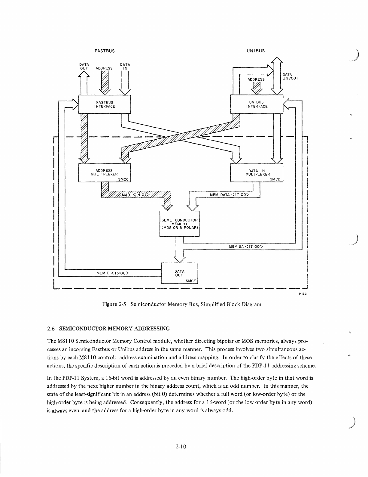
2.6 SEMICONDUCTOR MEMORY ADDRESSING
<15:00>
Figure
2-5
Semiconductor Memory Bus, Simplified Block Diagram
SEMI-CONDUCTOR
MEMORY
(MOS
OR
B I POLAR)
DATA
OUT I
~~
IN
DATA
MULIPLEXER
MEI'v1
DATA
<17:00>
MEM
SA
<17:00>
________________
SMCD
~
11-1321
The
M811
0 Semiconductor Memory Control module, whether directing bipolar or
or
cesses an incoming Fastbus
M811
tions by each
actions, the specific description
In the PDP-II
addressed by the next higher number in the binary address count, which
state
of
the least-significant bit in an address (bit 0) determines whether a full word (or low-order byte)
high-order byte
is
always even, and the address for a high-order
0 control: address examination and address mapping. In order to clarify the effects
System, a 16-bit word
is
being addressed. Consequently, the address for a 16-word (or the low order byte in any word)
Unibus address in the same manner. This process involves two simultaneous ac-
of
each action
is
addressed
is
preceded by a brief description
by
an even binary number. The high-order
is
an odd number. In this manner, the
byte
in any word
2-10
is
always odd.
MOS
memories, always pro-
of
of
the PDP-II addressing scheme.
byte
in
that
word
or
the
these
is
For
example:
Typical address for a full l6-bit word
Address for the high-order byte in the same word
at
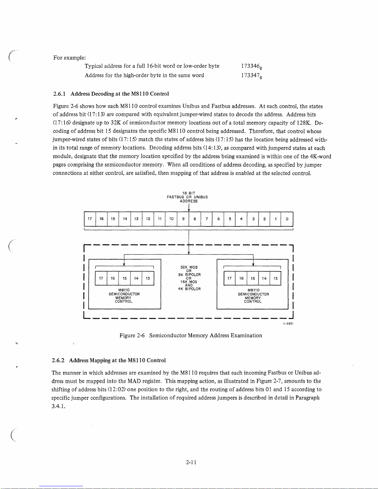
2.6.1 Address Decoding
Figure
2-6
shows how each M8l1 0 control examines Unibus and Fastbus addresses. At each control, the states
of
address bit
07:
16)
coding
jumper-wired states
in its total range
module, designate that the memory location specified by the address being examined
pages comprising the semiconductor memory.
connections at either control, are satisfied, then mapping
(I
7:
13)
designate up to 32K
of
address bit
of
of
memory locations. Decoding address bits
the M8110 Control
are compared with equivalent jumper-wired states
of
semiconductor memory locations out
15
designates the specific M81l 0 control being addressed. Therefore, that control whose
bits
(I
7:
15)
match the states
or
When
FASTBUS
of
ADDRESS
low-order byte
address bits
<I
4:
all
conditions
of
that address
18
BIT
OR
UNIBUS
(I
13),
of
of
7:
173346
173347
to
decode the address. Address bits
a total memory capacity
15)
has the location being addressed with-
as
compared with jumpered states at each
address decoding,
is
enabled at the selected control.
8
8
of
is
within one
as
specified by jumper
128K.
of
the 4K-word
De-
1,6
15
1
1,,1
1,7
I
r-----------
I
I I
I
17
I
I
I
I
I I
~
16
15
I I I
M8110
SEMICONDUCTOR
MEMORY
CONTROL
14
13
1,2
13
I
1" 1
I
10
I 9 t B I 7 I 6 I 5 I • I 3 I 2
-----------l
32K
MOS
OR
8K
BIPOLOR
OR
16K
MOS
AND
4K
BIPOLOR
I
L
_____________________
Figure
2-6
Semiconductor Memory Address Examination
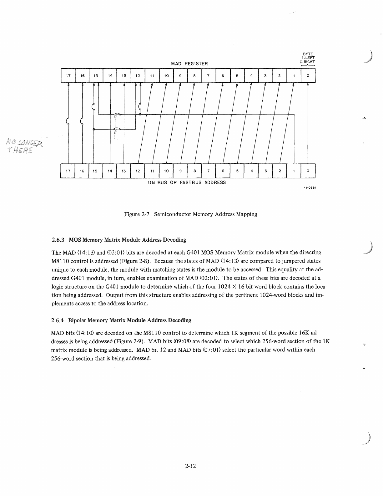
2.6.2 Address Mapping at the
The manner in which addresses are examined by the M8l1
dress must be mapped into the
shifting
specific jumper configurations. The installation
3.4.1.
of
address bits
<I
M8110 Control
MAD
register. This mapping action,
2:02) one position to the right, and the routing
of
required address jumpers
0 requires
I,
I 0 I
I
I
I
I
1
I
I
I
I
17
I
~
16
15
14
I I 1
M8110
SEMICONDUCTOR
MEMORY
CONTROL
13
I
J
1/-0831
that
each incoming Fastbus or Unibus ad-
as
illustrated in Figure 2-7, amounts to the
of
address bits
is
described in detail in Paragraph
Oland
15
according to
(
2-11
MAD
REGISTER
BYTE
1:LEFT
O:RIGHT
~
MOS
2.6.3
The
MAD
M8110 control
unique
dressed
Memory Matrix Module Address Decoding
<14:
13)
and
is
addressed (Figure 2-8). Because the states
to
each module, the module with matching states
G401 module, in turn, enables examination
logic structure on the
tion being addressed.
UNIBUS
Figure
2-7
<02:01)
G401
bits are decoded at each
module to determine which
Output from this structure enables addressing
OR
FASTBUS
Semiconductor Memory Address Mapping
G401
of
MAD
plements access to the address location.
2.6.4 Bipolar Memory Matrix Module Address Decoding
MAD
bits
04:
10)
are decoded
dresses
is
being addressed (Figure 2-9).
matrix module
is
being addressed.
256-word section that
is
on
the M8110 control to determine which
MAD
being addressed.
MAD
bits (09:08) are decoded to select which 256-word section
bit 12 and
MAD
ADDRESS
MOS
Memory Matrix module when the directing
of
MAD
04:
13)
are compared to jumpered states
is
the module to be accessed. This equality
(02: 01). The states
of
the four 1024 X 16-bit word block contains
of
the pertinent 1024-word blocks and im-
IK
of
these bits are decoded
segment
of
the possible 16K ad-
\1-0681
at
bits (07:01) select the particular word within each
the ad-
at
the
loca-
of
the
a
1K
2-12

r-
__________
COLUMN
~A~
ADDRESS
__________
ROW
~y~------------~A~------------~)
ADDRESS
15
ADDRESS
1
OF
4
4K
MATRIX MODULES
ADDRESS
1
OF
2
CONTROLS
M8110
CONTROLr-----------------~
MEMORY ADDRESS REGISTER
ADDRESS
1
OF
WORD
1024
LOCATIONS
-----,
4K
G401 MEMORY
MATRIX MODULE
4K
G401 MEMORY
MATRIX MODULE
(MAD)
I
I
I
ADDRESS
10F4-1K
MEMORY BLOCKS
16K
'--------------'
Figure 2-8
4K
G401 MEMORY
MATRIX MODULE
4K
G401 MEMORY
MATRIX MODULE
MOS
MOS
Memory Matrix Address Examination
2-13
11-1322
 Loading...