

Digital Equipment KXJ11-CA Installation Manual
EK-KXJCA-IN-001
KXJ11-CA
Single-Board
Computer.
Installation
Guide
EK-KXJCA-IN-001
KXJ11-CA
Single-Board
Computer
Installation
Guide
Prepared
of
Digital Equipment Corporation
by
Educational Services
1st
Edition, December 1986
Copyright
All
Rights Reserved.
Printed in
The reproduction of this material, in
information, contact
Corporation, Marlboro, Massachusetts
The
@ 1986 by Digital Equipment Corporation.
U.S.A.
part
or
whole, is strictly prohibited. For copy
the
Educational Services Department, Digital Equipment
01
7 52.
information in this document is subject
to
change without notice. Digital
Equipment Corporation assumes no responsibility for any errors
this document.
The
following are
trademarks of Digital Equipment Corporation,
Massachusetts 01754.
mamaD!DTM
DEC
DECmate
DECUS
DECwriter
DIBOL
KA630
MASSBUS
MicroVAX
PDP
P/OS
Professional
Q-Bus
Rainbow
RSTS
VAX
VAXELN
VMS
RSX VT
RT
Work Processor
UNIBUS
that
may
appear in
Maynard,
Contents
Chapter 1 - Introduction. . . . . . . . . . . . . . . . . . . . . . . . . . . . . .
Chapter 2 - Selecting Operating Features. . . . . . . . . . . . . . . .
2.1 Boot/Self-Test Switch. . . . . . . . . . . . . . . . . . . . . . . . . . . . . . . .
2.2 Q-Bus Size . . . . . . . . . . . . . . . . . . . . . . . . . . . . . . . . . . . . . .
2.3 Q-Bus Base Address Selection . . . . . . . . . . . . . . . . . . . . . . . . . .
2.4 DMA Requests
2.5 Locked Instruction Enable
2.6 BREAK Enable Selection
2.
7 HALT Option Selection . . . . . . . . . . . . . . . . . . . . . . . . . . . . . . . . 2-14
2.8 Power-Up Option Selection
2.9 PROM Addressing
2.10 SLU1 Baud Rate
2.11 SLU1
2.12
2.13 SLU2 Channel A Receiver
2.14
2.15
2.16 Real-Time Clock
Transmitter
SLU1 Receiver
SLU2 Channel B Transmitter
SLU2 Channel B Receiver
......................................
...............................
...............................
..............................
...................................
....................................
...................................
.....................................
..............................
............................
..............................
Interrupt
..............................
Chapter 3 - Power Supply Considerations. . . . . . . . . . . . . . . .
..
..
..
..
..
..
1-1
2-1
2-3
2-8
2-9
2-11
2-12
2-13
2-15
2-16
2-17
2-19
2-20
2-21
2-22
2-24
2-25
3-1
Chapter 4 - Installing the KXJ11-CA
4.1 Edge Connector Pin Assignments . . . . . . . . . . . . . . . . . . . . . . . .
Chapter 5 - Connectors and External Cabling . . . . . . . . . . . . .
5.1 Parallel I/O Interface (J4) . . . . . . . . . . . . . . . . . . . . . . . . . . . . .
5.2 Serial
5.3 Loopback Connectors. . . . . . . . . . . . . . . . . . . . . . . . . . . . . . . .
110
Lines (J1,
Chapter 6 - Diagnostics. . . . . . . . . . . . . . . . . . . . . . . . . . . . . .
6.1
Error
Detection and Reporting with the
6.2 Diagnostic Testing with
in
a Backplane. . . . . . . . .
J2,
J3) . . . . . . . . . . . . . . . . . . . . . . . . . . . .
XXDP+.
LEDs.
. . . . . . . . . . . . . . . . . . . . . . . .
iii
. . . . . . . . . . . . . . . .
..
..
..
..
..
..
..
..
..
4-1
4-3
5-1
5-1
5-2
5-8
6-1
6-1
6-3
Figures
2-1
KXJ11-CA
2-2
Memory Mapping - PROM in
2-3
Memory Mapping - PROM in High Menlory . . . . . . . . . . . . . . . . .
2-4
Boot/Self-Test Switch. . . . . . . . . . . . . . . . . . . . . . . . . . . . . . . .
2-5 Q-Bus Size Selection . . . . . . . . . . . . . . . . . . . . . . . . . . . . . . . .
2-6 Q-Bus Base Address Selection . . . . . . . . . . . . . . . . . . . . . . . . . . . . 2-10
2-7
DMA Requests
2-8
Locked Instruction Enabie
2-9
BREAK Enable
2-10 HALT Option Selection
2-11
Power-Up Option Selection. . . . . . . . . . . . . . . . . . . . . . . . . . . . . . 2-15
2-12
PROM Addressing
2-13
SLU1 Baud Rate
2-14
SLU1
SLU1 Receiver
2-15
2-16 SLU2 Channel A Receiver
SLU2 Channel B Transmitter
2-17
2-18 SLU2 Channel B Receiver
2-19 Real-Time Clock Interrupt
4-1
Backplane Installation . . . . . . . . . . . . . . . . . . . . . . . . . . . . . . .
4-2
Using
5-1
Parallel
5-2
J2
and
5-3
J1
Pin Assignments (40-Pin)
5-4
Loopback Connectors. . . . . . . . . . . . . . . . . . . . . . . . . . . . . . . .
Jumper
Layout. . . . . . . . . . . . . . . . . . . . . . . . . . . . .
Low
Melnory. . . . . . . . . . . . . . . . . .
......................................
...............................
.....................................
................................
...................................
....................................
Transmitter
...................................
.....................................
..............................
............................
..............................
..............................
Grant
Cards . . . . . . . . . . . . . . . . . . . . . . . . . . . . . . . . .
110
Interface Pin Assignments . . . . . . . . . . . . . . . . . . . . .
J3
Pin Assignments (lO-Pin) . . . . . . . . . . . . . . . . . . . . . . .
......................
: . . . . .
..
..
..
..
..
..
..
..
..
..
..
2-1
2-3
2-4
2-5
2-8
2-11
2-12
2-13
2-14
2-16
2-17
2-19
2-20
2-21
2-23
2-24·
2-25
4-1
4-2
5-1
5-3
5-3
5-8
Tables
2-1
Factory Shipped
2-2
Boot/Self-Test Switch Functions . . . . . . . . . . . . . . . . . . . . . . . . .
2-3
Q-Bus Base Address Selection . . . . . . . . . . . . . . . . . . . . . . . . . .
2-4
SLU1 Baud Rate Jumpering
4-1
KXJ11-CA Pin
5-1
RS422/RS423 Interface to
5-2
RS232-C Interface to
5-3
CCITTN.35 Interface to
6
..
1 LED Display Definitions. . . . . . . . . . . . . . . . . . . . . . . . . . . . . .
Jumper
Configuration . . . . . . . . . . . . . . . . . . . . .
..............................
Identification.
J1
J1
. . . . . . . . . . . . . . . . . . . . . . . . . . . . . .
J1
. . . . . . . . . . . . . . . . . . . . . . . . . . . .
. . . . . . . . . . . . . . . . . . . . . . . . . .
. . . . . . . . . . . . . . . . . . . . . . . . . . .
..
..
..
..
..
..
..
..
2-2
2-5
2-9
2-18
4-3
5-4
5-6
5-7
6-2
iv
Chapter 1
Introduction
This guide describes how to install
NOTE
Before changing
sure
the
ify
that
the
Installation includes
1.
Selecting operating characteristics
(Chapter
2.
Determining power supply requirements (Chapter
3. Installing
4.
Selecting and connecting cables from serial
external
5.
Verifying proper operation (Chapter
jumpers
the
2)
the
devices (Chapter
the
factory shipped
match
module is operating as described in Section 6.2.
following activities.
board into a backplane (Chapter
the
KXJ
11-CA module.
jumper
the
jumpers shown in Figure 2-1, and ver-
and
5)
6)
configuration,
installing appropriate jumpers
3)
4)
and
parallel
make
110
interfaces to
1-1

Chapter 2
Selecting Operating Features
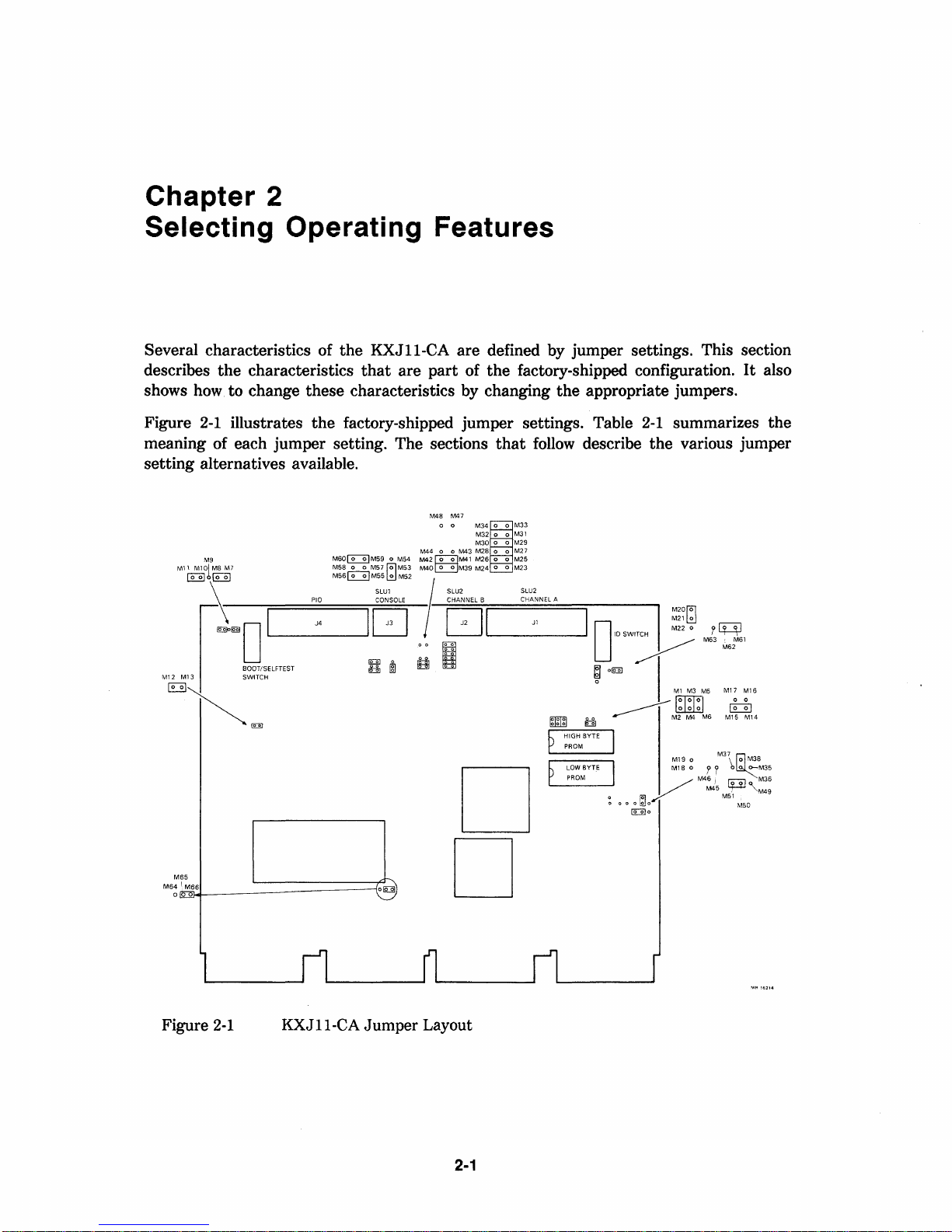
Several characteristics of the KXJ11-CA
describes the characteristics that
shows
Figure
how
to change these characteristics
2-1
illustrates the factory-shipped jumper settings. Table
are
are
defined
part
of the factory-shipped configuration.
by
changing the appropriate jumpers.
meaning of each jumper setting. The sections that
setting alternatives available.
M48
M47
0 0
M33
M34
M32 0 0 M31
M30
0 0
M44 0 0
M60~M59
M58
M56
0 M54
0 0 M57
fOlM53
~
M55 ~ M52
SLUI ! SLU2 SLU2
I
r:~cel
M43 M28
M42~M41
M40~M39
r:'"
M26
M24
II
M29
0 0 M27
0 0
M25
0 0
M23
D
by
jumper settings. This section
2-1
summarizes the
follow
'"~:""
describe the various jumper
M20~
I
010
SWITCH
;
.§]
g
_____
~
~
0 0 0
~~~
I~
I
...---f
1
FI:[oI'
I
000
M2 M4
Ml9
Ml8
V
~o
1:2:2]0
: r
M63 M61
M6
0 0
0
??
M461
M45
~
M62
M';:"
Ml5
M37~
M51
~
\
f"O"Ol
'+-+-'
M50
It
M14
M38
O-M35
'\';149
also
M36
M65
M64 I M66
o 0
Figure
2-1
KXJII-CA
Jumper
D
Layout
2-1
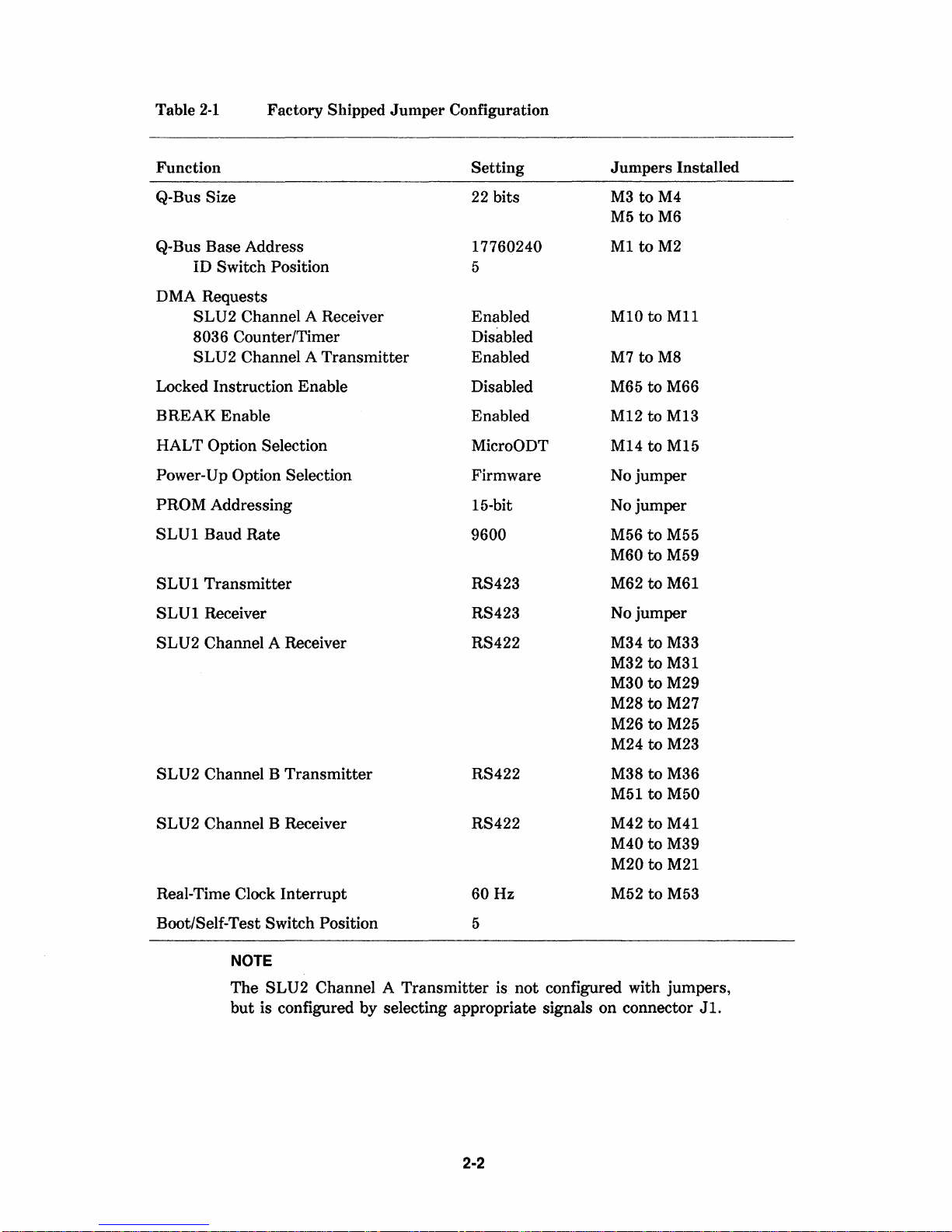
Table
2-1
Factory
Shipped JUlnper Configuration
Function
Q-Bus Size
Q-Bus
Base
Address
Switch Position
ID
DMA Requests
SLU2
Channel A Receiver
8036 Counter/Timer
SLU2
Channel A
Transmitter
Locked Instruction Enable
BREAK
HALT
Enable
Option Selection
Power-U p Option Selection
PROM
SLU1
SLU1
SLU1
Addressing
Baud
Rate
Transmitter
Receiver
Setting
22 bits
17760240
5
Enabled
Disabled
Enabled
Disabled
Enabled
MicroODT
Firmware
15-bit
9600
RS423
RS423
Jumpers
M3
to
M4
to
M5
M1
M10
M7
M65
M12
M14
No
No
M56
M60
M62
No
M6
to
M2
to
to
M8
to
to
to
jumper
jumper
to
to
to
jumper
Installed
MIl
M66
M13
M15
M55
M59
M61
SLU2
SLU2
SLU2
Real-Time Clock
Channel A Receiver
Channel B
Transmitter
Channel B Receiver
Interrupt
Boot/Self-Test Switch Position
NOTE
The
SLU2
but
is configured
Channel A
by
RS422
RS422
RS422
60Hz
5
Transmitter
is
not
configured with
selecting appropriate signals
M34
to
to
M32
M30
to
to
M28
to
M26
to
M24
M38
to
to
M51
M42
to
M40
to
M20
to
M52
to
on
connector J1.
M33
M31
M29
M27
M25
M23
M36
M50
M41
M39
M21
M53
jumpers,
2-2
2.1
Boot/Self-Test Switch
The boot/self-test switch is a I6-position switch
than
to execute firmware (rather
1.
It
determines
how
MicroODT) upon power-up.
the
KXJII-CA
will
exists, including whether or not self-tests
2.
KXJJJ-CA
It
determines whether special
Single-Board Computer User's Guide, EK-KDJCA-UG-OOI).
interrupt
user code or by firmware.
3.
It
determines where in memory
two alternatives ated with
low
low
memory
and high PROM mapping are shown in Figures
the
or
high memory. The memory maps associ-
respectively.
17777777
17774000
17773777
17773000
17772777
17770000
17767777
17760000
17757777
POWER
UP
MONITOR
DIAGNOSTICS
AND
that
is used if
act
when a special
will
the
board is configured
It
has
three
functions.
interrupt
condition
run (see Section 3.5, The
handling is performed either by
on-board PROM is mapped. There are
2-2
and 2-3,
1
I/O PAGE
1
,.1".
,."
2200000
2177777
2174000
2173777
2173000
2172777
2170000
2167777
2160000
2157777
2000000
1777777
7
7777
l~p'Ror~/RAM
o
• ADDRESSES 77777-0 MATCH ADDRESSES 2077777-2000000
Figure
2-2
NXM
POWER
MONITOR
DIAGNOSTICS
USER PROM
RAM
SPACE
Memory Mapping - PROM in
UP
AND
":_
,.~
"r"
T
NATIVE
FIRMWARE
1
\1R-17263
Low
Memory
2-3
17777777
17774000
17773777
17773000
17772777
17770000
1776777
1776000
1775777
220000
217777
2174000
217377
217300
217277 7
217000
216777
216000
215777
200000
177777 7
7
0
7
,.1.-
....
0
7
7
0
0
7
0
7
0
POWER
UP
MONITOR
DIAGNOSTICS
MONITOR
DIAGNOSTICS
AND
NXM
POWER
UP
AND
USER PROM
I
I
/0
PAGE
1
....
1.-
I'i""
I
NATIVE
FIRMWARE
1
0
Figure 2-3
RAM
MR-17262
Memory Mapping -
PROM in High Memory
2-4
The
location of
the
functions associated with each switch position.
the
boot/self-test switch is shown in Figure 2-4. Table 2-2 summarizes
BOOT/SELF-
TEST SWITCH
Table
2-2
Figure
2-4
Boot/Self-
D
..
. .
..
Boot/Self-Test Switch
Test
Switch
Functions
.
DI
....
..
..
..
..
..
. ...
D
D
..
.
..
.
'0
..
..
.....
...
MR-16215
Switch
Position
0
1
KXJII-CA
Special
User
executed. No self-tests
performed.
User
executed. Auto self-tests
performed.
Interrupt
PROM application code is
PROM
Response
are
application code is
are
2-5
Special
Interrupt
Handling
Firmware
Firmware
PROM
Mapping
Low
Low
Table
2-2
Switch
Boot/Self-Test Switch Functions (Cont)
KXJII-CA
Position Special
Interrupt
Response
Special
Interrupt
Handling
PROM
Mapping
2 User PROM application code is
3
executed. Auto self-tests
performed.
checksum
The
user
test
is also performed.
Application code is booted from Firmware
a
TU58 via
are
performed,
SLUl.
then
are
(P)ROM
Auto self-tests
the
TU
58
primary bootstrap is executed.
4
5
6
7
MicroODT is entered. No self-tests
are
performed.
Auto self-tests
The
KXJII-CA
the
arbiter
No self-tests
The
KXJII-CA
from
the
Auto self-tests
are
performed.
awaits command from
via TPRO.
are
performed.
awaits a command
arbiter via TPRO.
are
performed
continuously. No application
code is booted or executed.
Loopback connectors (see
Section 5.3)
for
these
are
tests.
installed
Firmware
Firmware
Firmware
Firmware
None
Low
High
High
High
High
High
8
9
10
11
12
User
PROM application code is
executed. No self-tests
are
performed.
User
PROM application code is
executed. Auto self-tests
are
performed.
User
PROM application code is
executed. Auto self-tests
performed.
checksum
The
user
test
is also performed.
are
(P)ROM
Application code is booted from
TU58 via
a
are
performed,
SLUl.
then
Auto self-tests
the
TU 58
primary bootstrap is executed.
MicroODT is entered. No self-tests
are
performed
2-6
User
Code
User
Code Low
User
Code
User
Code High
User
Code High
Low
Low
Table
2-2
Switch
Position
Boot/Self-Test
KXJII-CA
Special
Interrupt
Switch Functions (Cont)
Response
Special
Interrupt
Handling
PROM
Mapping
13
14
15
Auto self-tests are performed.
The KXJ11-CA awaits a command
from
the
arbiter via TPRO.
No self-tests are performed.
The KXJ11-CA awaits a command
the
from
arbiter via TPRO.
Auto self-tests are performed
continuously. No application
code is booted or executed.
Loopback connectors (see
Section
5.3~
are installed
for these tests.
NOTES
1.
Switch position 5 is
2.
The encoded value of
able in
the
KXJCSRB register in bits < 7:4
the
factory-shipped configuration.
the
boot/self-test switch position is avail-
switch position 1 would be encoded as
<7:4>.
3.
The
user
(P)ROM checksum
highest word address of
checksum
dress of
and
checked according
test
looks for a checksum
the
firmware PROM. Either checksum is calculated
to
test
user
(P)ROM. Similarly,
the
following DECPROM algorithm:
User Code
User Code
None
>.
For example,
0001 in KXJCSRB
looks for a checksum
the
firmware
at
the
highest word ad-
at
High
High
High
the
CHECKSUM = 0
FOR
I = number of PROM addresses to be checksumed
DO CHECKSUM = CHECKSUM + contents of address
(high order carry from addition is discarded)
CHECKSUM = ROTATE_LEFT_ONE_BIT
bit1
~
bit2, .... ,bit15 ~ bitO)
4.
Special interrupt handling can be performed by user code in
NEXT I
(bitO
switch positions 8-15. This function is useful in applications
that
need
to
the
or
tions
continue running after
Q-Bus signal BINIT has been asserted. For switch posi-
0 through
7,
special interrupt handling is done by
the
Q-Bus signal BHALT
firmware.
5.
If
the
KXJ11-CA is in standalone mode, switch positions
13, and 14 should not
be used. These positions cause
KXJ 11-CA to idle and wait for a command. In standalone
mode,
ter
command
KXJ11-CA
that
will
will
never come.
idle indefinitely, waiting for
the
2·7
~
an
bit1,
5,
6,
the
arbi-
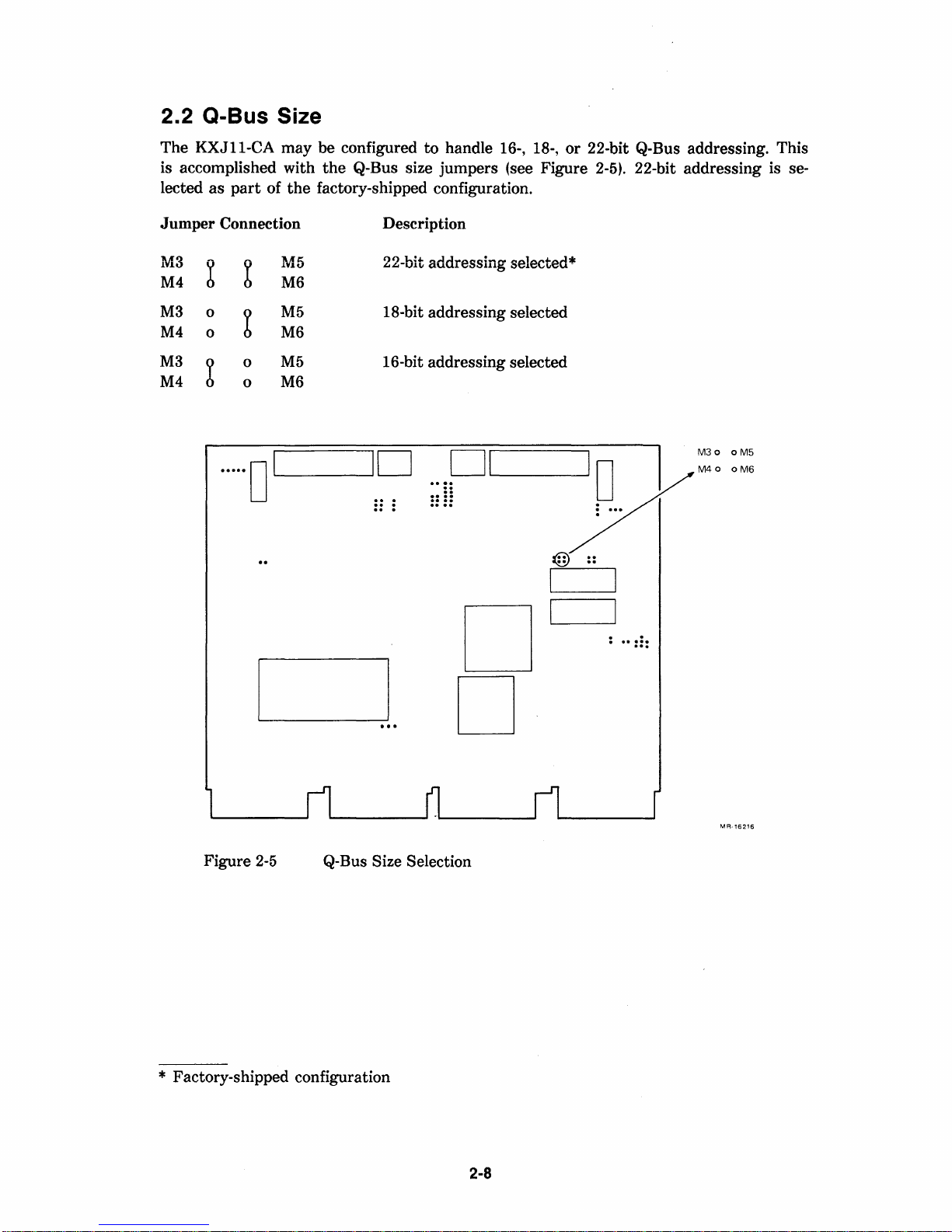
2.2 Q-Bus Size
The
KXJ11-CA
is accomplished with
lected
as
part
of
may
the
be
configured
the
Q-Bus size
factory-shipped configuration.
to
handle 16-, 18-,
jumpers
(see Figure 2-5). 22-bit addressing is se-
or
22-bit Q-Bus addressing. This
Jumper
M3
M4
M3
0
M4
0
M3
X
M4
Connection Description
b b
b
0
0
.....
0
M:5
M6
M5
M6
M5
M6
1
L--
__
22-bit addressing selected*
18-bit addressing selected
16-bit addressing selected
ID
. . .
....
..
..
..
01
..
..
..
..
D
10
:
..
:::
M30
M40
oM5
oM6
Figure
2-5
Q-Bus Size Selection
* Factory-shipped configuration
D
MR-16216
2-8
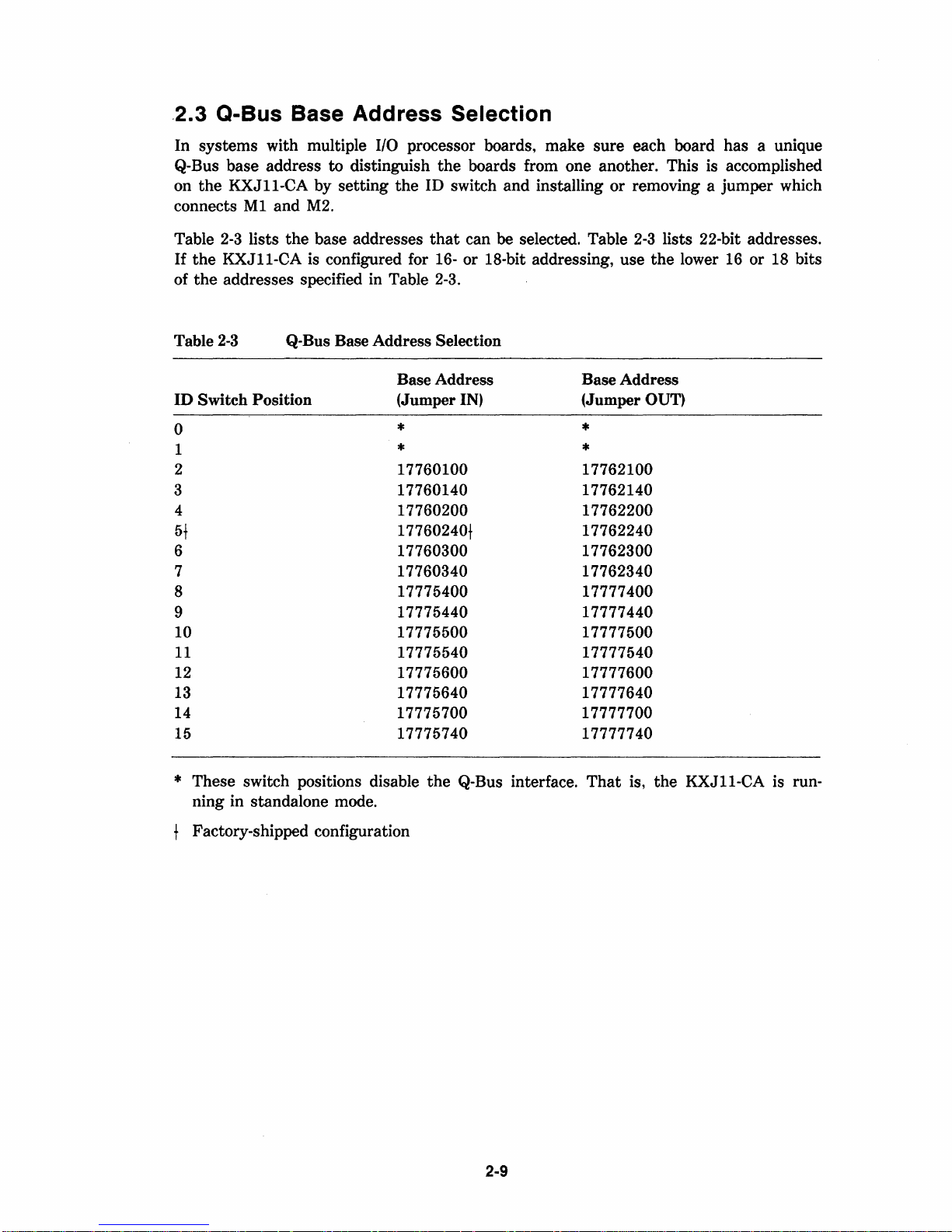
.2.3 Q-Bus Base Address Selection
In
systems
Q-Bus base address
on
the
connects
Table
If
the
of
the
with multiple I/O processor boards,
to
distinguish
KXJII-CA
Ml
2-3
lists
KXJII-CA
addresses specified in Table 2-3.
by
setting
and
M2.
the
base addresses
is configured for 16- or 18-bit addressing, use
the
ID switch
the
that
boards from one another. This is accomplished
and
installing
can
be
selected. Table
make
sure
or
each board
removing a
2-3
lists 22-bit addresses.
the
has
jumper
lower 16 or 18 bits
a unique
which
2-3
Table
ID
Switch Position
0
1
2
3
4
5t
6 17760300 17762300
7 17760340 17762340
8
9
10 17775500 17777500
11
12 17775600 17777600
13 17775640 17777640
14
15 17775740 17777740
* These switch positions disable
ning in standalone mode.
Q-Bus Base Address Selection
Base Address
(Jumper IN) (Jumper
* *
* *
17760100 17762100
17760140 17762140
17760200 17762200
17760240t
17775400 17777400
17775440 17777440
17775540 17777540
17775700 17777700
the
Q-Bus interface.
Base Address
17762240
That
is,
OUT)
the
KXJII-CA
is run-
Factory-shipped configuration
2-9
 Loading...