

Page 1
~TAA
U
.........
user's
guide
IIIIIII
Page 2

~TAA
U
.........
user's guide
DEC-II-HGT44-A-D
digital equipment corporation · maynard. massachusetts
Page 3
Copyright © 1973 by Digital Equipment Corporation
1st Edition, December 1973
. The material in this manual
purposes and
Digital Equipment Corporation assumes no responsibility
manual.
is
subject to change without notice.
tOI
any errors which may appear in this
Printed
The foHowing are trademarks
in
is
U.S.A.
of
for informational
Digita1
Corporation, Maynard, Massachusetts:
Equipment
DEC
FLIP
CHIP
DIGITAL
UNIBUS
PDP
FOCAL
COMPUTER
LAB
Page 4
CONTENTS
Page
1.1
1.2
1.3
1.3.1
1.3.1.1
1.3.1.2
1.3.1.3
1.3.1.4
1.3.1.5
1.302
1.3.3
1.3.4
1.3.5
1.3.6
1.3.7
1.4
1.4.1
1.4.2
1.4.3
1.4.4
1.4.5
1.4.6
2.1
2.1.1
2.1.2
2.1.3
2.1.4
2.1.5
2.1.5.1
2.1.5.2
3.1
3.1.1
3.1.1.1
3.1.2
4.1
4.2
4.3
4.4
4.5
4.5.1
4.5.2
4.5.3
4.6
4.6.1
4.6.2
4.6.3
PURPOSE
GENERAL
SYSTEM DESCRIPTION
EQUIPMENT
OPERATING CONTROLS
GT44
GT44 PROGRAMMING CONCEPT .
IMPORTANT
PDP-l1i40
VT11 INSTRUCTION SET
PROGRAMMING
PROGRAMMING RESTRICTIONS
AND
SCOPE
DESCRIPTION
PDP-11/40 Computer
Unibus
KD11-A Processor
KY11-D Programmer's
M F
ll-L
Power System
VT11 Graphic Display Processor .
VR17
Cathode
375
Light
Pen
LA30-S DECwriter
RK05
Disk Drives and RK11-D Disk Drive Control
BM792YB Bulk Storage Bootstrap Loader
SPECI
PDP-l1/40
VT11 Graphic Display Processor
VR17
375
LA30
R K05 Disk Drive
PDP-11/40
VR
17
LA30
R K05 Disk Drive
Circuit Breakers and
OPERATING PROCEDURES .
GT
44
GT44 Failure Procedures
Initializing the Display Processor
Display File
Application
Stop
Display File
Non-Flicker Display
Processor
CRT Display
Light
Pen
DECwriter
CRT Display
DECwriter
Circuit Breakers
Fuses
Start
Up
Duplicating the System Disk
ADDRESSES
INSTRUCTION SET .
EXAMPLES
of
and
Sync, Microcoding .
Changes
..........
AND
............
Core Memory
......
Ray
Tube
..............
and
DL
FICATIONS
.....
Monitor
.........
and
DL
and
R K
AND
...........
Monitor
...
..
. . . .
Fuses
..........
Procedures
..........
the Stop
Interrupt
.....
........
OPERATION
......
Console
..
Monitor
11
Asynchronous Line Interface
..
11
Asynchronous Line Interface
l1-D
Controller . . . . .
INDICATORS
. .
...
....
..
.
.
1
2
.
.
2
2
3
3
.
4
5
....
.
.
.......
5
5
6
6
..
.....
7
7
.
7
7
8
. . . . .
..
8
9
9
.....
.
....
.
.
.
.
..
..
10
10
12
12
12
12
12
12
12
15
15
16
17
18
20
· 20
· 20
20
20
21
· 22
.22
·
22
· 28
iii
Page 5
CONTENTS (Cont)
Page
4.7
4.7.1
4.7.2
4.7.3
4.7.4
4~8
APPENDIX A
APPENDIX B
Figure No.
1
2
3
4
5
6
7
8
9
ADVANCED
Subroutines
Light
Special Characters
Edge
GT44 SOFTWARE
CHARACTE
BM792-YB
Relationship
PDP-11/40 Programmer's Console
LA30
K05
R
Memory
Instruction Word Functions
Data Word Formats
Non-Flicker Display
Subroutining Example
PROGRAMMING TECHNIQUES
Pen
Interaction
Violations
..
R CODES
BULK
STORAGE BOOTSTRAP
ILLUSTRATIONS
of
GT44 Components
DECwriter Console
Controls and Indicators
Layout
Example
as
Determined
.........................
Title
to
the Unibus
by
Vector
LOADER
Quantity
PROGRAM LISTING
and Magnitude
.
28
28
30
30
31
31
Page
11
13
14
17
23
24
29
30
Table No.
1
2
3
RK11 Registers
Controls and
Recommended GT44 Mnemonics
Indicators
TABLES
Title
Page
6
14
26
iv
Page 6
GT44 USER'S GUIDE
Page 7
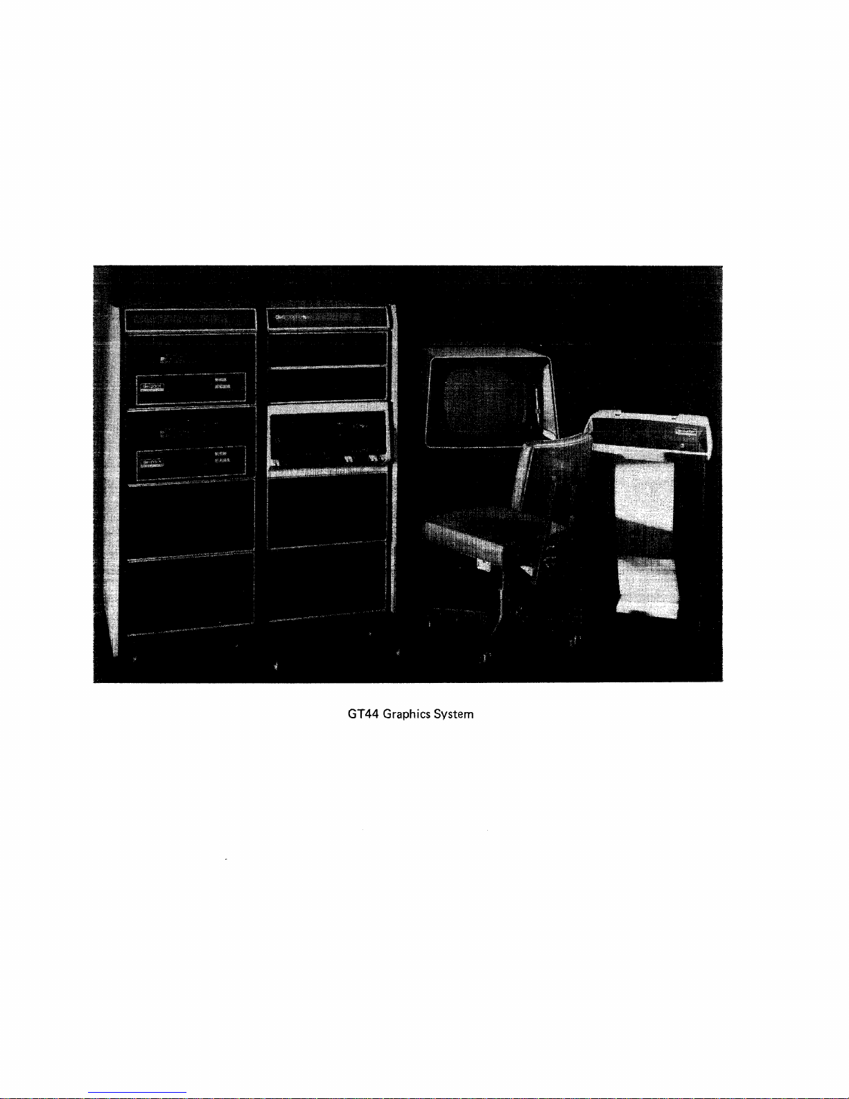
GT44 Graphics System
Page 8
1.1
PURPOSE
This guide describes the operation of
System.
description
AND
SCOPE
The
following information
and
operation,
equipment
the
GT44
Grapnlcs
is
included: system
specifications, controls and indicators, start-up procedures, and programming
techniques.
the
functional units
System,
user, arid
more detailed sources
It
is
the
intention
that
to
present in brief, information
to
reference, where necessary, additional and
of
of
this guide
make
up
information.
to
the
GT44 Graphics
of
relevance
tie
together
to
the
1.2 GENERAL DESCRIPTION
The
DECgraphic
ful disk-based PDP-11/40
been added.
require a visual display, a high
capability, and mass data storage. With its
the
GT44 has access
any
time. Its 16K
operating system such as RT-11/GT,
room
for user programs.
combination and
interaction. Because graphic capabilities have been added
the
software system, processor
The
11/40
GT44
to
which graphic capabilities have
GT44
is
designed for applications
to
2.4
million 16-bit words
of
core memory allows use
The
the
DECwriter provide
Graphics System
order
of
two
yet
leaves adequate
CRT
monitor/light
for
and
display utilization
is
a power-
that
computation
disk drives,
of
data
at
of
an
pen
user-system
to
is
simplified.
1.3 SYSTEM DESCRIPTION
ponents:
a.
PDP-11/40
Computer
1. Unibus
2.
KD11
3. KY11-D Programmer's Console
4. MF11-L
5. Power
b.
VT11 Graphic Display Processor
c.
VR17
CRT
Display Monitor
375
d.
e.
Light Pen
LA30 DECwriter with DL
Interface
f.
Two
RK05 Disk Drives with RK11-D Control-
ler
g.
BM792YB Bulk Storage Bootstrap Loader
ROM.
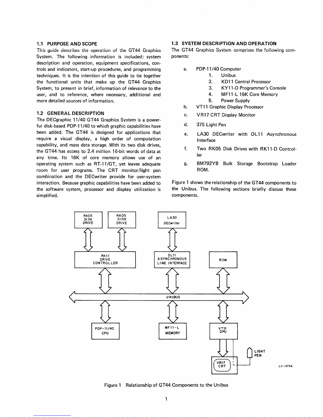
Figure 1 shows
the
Unibus.
the
relationship
The
following sections briefly discuss these
components.
AND
OPERATION
Central Processor
16K
Core Memory
Supply
11
Asynchronous
of
the
GT44
components
to
RK05
DISK
DRIVE
CONTROLLER
RK11
DRIVE
PDP-11/40
CPU
RK05
DISK
DRIVE
LA30
DECwriter
DL11
A SYNC HRONOUS
LI
NE INTERFACE
UNIBUS
MF11-L
MEMORY
ROM
VT11
DPU
LIGHT
PEN
Cp-0156
Figure 1 Relationship
of
GT44
Components
to
the
Unibus
Page 9
1.3.1
PDP-ll/40
The
PDP-ll/40
microprogrammed
and
instructions and
PDP-l1/40
which can directly address
memory.
(including processor, core memory, and peripherals)
performed
of
device-to-device transfers can be
2.5
peripherals are linked
and
Therefore,
also be applied
enabling peripheral device registers
the
Subsequent
tion
1.3.1.1 Unibus munication between system
data,
transfers
of
repertoire
and
interfaces. The asynchronous nature
also eases design
operations
All
the
bus concept,
million words per second. All system
all peripherals are in
processor as flexibly as memory.
of
the
address,
to
the
bus an
design
Computer
is
a 16-bit general purpose, parallel logic,
computer
contains a multiple
communication
on
a single high-speed bus,
all
instructions applied
to
paragraphs present a brief functional descrip-
PDP-ll/40.
The
and
control lines,
occur between all units
important
of
bus operations
economy,
and
is:
using single
2's
complement
word
up
among system
all
peripherals are compatible, and
accomplished
by
the
Unibus and power connectors,
the
basic system address space.
data
in
peripheral device registers,
Unibus provides high-speed com-
components.
factor
in
is
flexible enough for speed
yet
provides a fixed specification for
operation.
and
double oper-
arithmetic.
instruction processor,
to
28K
words
of
components
the
Unibus. Because
at
the
components
to
data
in
memory
to
be manipulated
With bidirectional
the
Unibus allows
on
the
bus, with control
these transfers.
of
The
repertoire
The
these operations
rate
of
The
core
and
can
data
fixed
bus
,
DATI, DATIP, DATO, DATOB - data operations
INTR, PTR (BR, NPR) - control operations
Full 16-bit words
transferred
DATI, DATIP operations transfer data into
DATO, DATOB operations transfer
When a device
requests use
make a Direct Memory Access (DMA) transfer of data
directly
processor intervention,
execution
address where an
Bus
(NPR)
INTR. A device can perform a
control
to
and force
control
for
via
on
the
a BR.
the
of
or
is
DMA
the
from
obtained
or
8-bit bytes
bus between
is
capable
bus, it
another
or
the
interrupt
or
under a Bus Request (BR) for an
of
information can be
the
master
and
slave.
The
the
master;
data
out
of
the
master.
of
becoming bus master and
is
for
one
of
two
purposes:
device
or
memory
to
INTeRrupt
processor
service
routine
under a Non-Processor Request
DMA
(lNTR) program
to
branch
is
after
without
to
a specific
located.
acquiring bus
is
of
by
to
the
Requests for
and
NPR lines. Transfer
another
which grants control
highest priority. NPRs are accorded higher priority
BRs.
Unibus data cycles, in
WAIT
completion
priority exceeds
The
operations
the
when no
The
Internal Unibus
Unibus
Unibus signals
module. A
system units
peripheral device removed
A
tions,
1.3.1.2
codes instructions; accepts, modifies, and
performs
the
sixteen hardware registers, eight
mable.
specifically used for processor operation: a program count-
er (PC)
arithmetic
and
The
of a variety
source
register,
operation
Because
modes, instruction set,
written
includes a
byte
words or bytes may be displayed on
console.
is
The
or
PDP-l1
next
bus master.
other
Unibus originates
from
complete
is
presented in
KDll-A
arithmetic
Unibus among external devices.
Two
and
autodecrement
eight non-programmable registers are used for storage
and
the
data.
of
in directly relocatable codes.
operands and provisions for
bus can be made
of
bus control from
made by
NPRs are serviced before
TRAP
/40
as
120-conductor
accumulators, index register, and
full
the
processor priority arbitration logic
of
the
addition
sequences.
of
the
current
that
of
the
processor.
processor has a special role
it performs
device has
and
the
processor
and
in
different mounting boxes
description
Processor-The
of
the
a stack
of
functions including: intermediate address,
destination
last
the
flexibility
complement
the
The
processor assumes bus control
control.
in
the
Terminator
to
17
grounds are carried
Mylar cable
from
of
the
the
PDP-11 Peripherals Handbook.
operations; and controls allocation
eight programmable registers are
pointer
registers.
data, a copy of
interrupt
of
and
DMA, PDP-11
of
at
any
time
on
the
one
device
bus
to
the
device having
and
immediately
to
specific times during
The
BRs are serviced upon
instruction
priority arbitration
processor with
module, which carries
the
the
Unibus, including specifica-
(SP);
the
vector address and console
hardware registers, address
instructions
if
the
in
next
system unit.
is
used
or
to
mounting box.
KD11-A Processor de-
outputs
The
processor contains
of
which are program-
remaining six serve as
autoincrement
the
/40
programs are
The
processor also
that
byte
swapping. Either
the
programmer's
after
requesting
bus control
to
select
the
M981
All
in
this
to
connect
connect
data;
instruction
manipulate
BR
the
than
the
56
one
to
a
of
2
Page 10
Any
of
the
eight
programmable
used
to
build last-in, first-out stacks.
processor (or
This stack-handling
the
program
subroutine
reentrant
The
Unibus serves
therefore,
which
requests use
non-processor
or
to
interrupt
to
branch
granted
device-to-device
tion.
A B R
instruction
calls
codes
there
device
to
by
the
and
system)
counter
and
and
must
becomes
of
the
transfer
program
an
processor
data
is
granted
allows
stack
pointer
capability
and
status
interrupts.
automatic
the
processor
nesting
be a priority
bus master. General!y, a device
bus
for
one
of
data
directly
execution
interrupt
at
the
service
end
transfers
by
the
the
device
processor task.
The
processor recognizes
each major level
attached
on
containing
each
electrically closest
devices
processor itself
on
the
same
is
programmable
therefore, a running
permissible
Additional
structure
interrupt
identifies itself,
automatically
device polling
tines.
priority
system
The
are
18-bit
word
Thus,
references up
interrupts.
speed
through
scheme. With
and a unique
selected
and
The
device
are
independent
behavior in response
Unibus addresses
direct
byte
length
and
while
the
PDP-11/40
to
four
sublevels. Many devices
major
level,
to
the
processor given
priority
program
and
power
the
use
of
vectored
by
the
permits
interrupt
to
to
generated
addresses, even
operational
word
32K
words
levels
level.
can select
are
the
nesting
priority
allow
real-time
logic
Processor can reference addresses
bytes).
In
addition
addressing space,
are reserved
ters. ! n the basic
to
for
peripheral
the
the
uppermost
PDP~
word
length
control,
11/40 configuration,
internal registers
One
register serves as a
for
automatic
permits save
word
This
and
and
in
conjunction
feature
of
subroutines.
all peripheral devices;
structure
of
two
reasons:
to
or
from
and
force
routine.
of
bus cycles
without
processor
processor interven-
at
to
interrupt
of
hardware
with
the
the
device
priority
The
priority
within
the
hardware
the
priority
added
to
PDP-11
/40
fully
interrupts,
interrupt
service
processor. This
of
device service rou-
and
service
dynamic
adjustment
conditions.
by
the
KD11-A Processor
though
the
is
16-bit
can
only
contain
(64K
bytes),
up
to
128K
constraint
4K
words
of
status,
and
stacking.
restore
allows
to
determine
to
make
memory,
the
processor
An
NPR
and
e~d
the
current
B Rs,
that
over
level
level
the
interrupt
vectored
the
routine
eliminates
routine
PDP-11/40
word
length.
address
the
KD11-A
words
on
address
data
all
address
can
with
true
allows
of
with
can
other
of
the
levels;
device
(256K
basic
space
regis-
be
of
a
is
an
be
is
of
is
of
references
space
references
16-bit
converted
773224
can
words
detailed
A
tained
to
the
(160000-177777)
with
bits
reference
to
a full
Consequently,
•
8
address
up
to
of
I/O device registers.
description
in
the
KD11-A Processor Manual, DEC-11-H KDAA-
uppermost
16
and
to
address
18-bit
the
28K
words
of
4K
words
of
16-bit
are
converted
17
always
1732248 is
to
set
to
automatically
I/O device register address
basic PDP-11
of
the
KD11-A Processor
core
/40
configuration
memory
A-D.
1.3.1.3
Programmer's
direct
stop,
Console displays indicate processor
contents
mounted
and
The
through a microprogram
The
diodes),
for
certain
for
the
whose
Console
and
descriptions
KD11-A Processor Manual, DEC-11-HKDAA-A-D.
1.3.1.4
GT44
capacity.
mounted
is
The
used
The
from
however,
structure,
processor
operand
a true arithmetic accumulator.
KY11-0
system
interface.
load,
modify,
of
the
as
the
is
connected
programmer's
console
switches,
the
control
Unibus
DEP
and
DATI
processor
priority
operation,
indicators,
of
MF11-L
contains
The
on a double
an
8K,
16-bit
backplane
to
accomodate a third
core
memory
the
processor
is
never bus master. Because
the
or
any
instructions,
Programmer's
Console
provides
The
console allows
examine,
address
front
to
panel
the
and
of
processor
console
control
contains
and
the
only
contact
switches. Console
operations
responds
supersedes all
for
EXAM.
to
through
a Console Bus
other
including
is
presented
console
an
MF11-L
logic circuits are
Core
Memory -The
MF11-L
consists
Core
system
word
memory
has
additional
optional
uses
the
Unibus
and
other
memory
other
every
can
master
location
Console -
the
programmer
step,
or
continue
operation
data
registers.
the
processor
by
two
interacts
with
located
indicators
bounce
operation
the
For
single-step
B R priorities.
descriptions
in Paragraph
Memory
of
2 MM11-L
unit
backplane.
consisting
unused slots
MM11-L
for
data
devices.
be
The
directly
device. Because
in
core
The
the
user
The
mounting
cables.
the
in
the
(tight-emitting
filtering circuits
does
processor: DATO
Request
of
all
2.1.
contained
PDP-11/40
with
Each MM11-L
of
three
which
8K
transfers
core
of
the
addressed
can
address
full
18-bit
1.
Thus,
of
and
4K
is
con-
KY11-D
with
to
start,
a program.
and
the
console
box
processor
processor.
require
operation,
(CBR)
controls
Detailed
in
the
in
the
16K
word
memories
modules.
can be
memory.
to
and
memory,
Unibus
by
the
of
double
function
as
a
a
is
3
Page 11
The memory does
it
is
always a slave device.
request use of
either a
BR
independent of
perform direct data transfers with memory
not
enter
the
The
the
Unibus,
and
or an NPR. Because
the
processor, any master device can
priority structure because
master device, however, can
thus
the
the
memory,
memory
without
through
is
completely
proces-
sor intervention.
1.3.1.4.1
graphs briefly describe
up
the
MF11-L, and MF11-LP Core Memory
MMll-L
the
MF11-L memory.
Core Memory -
the
MM11-L memories, which make
For
more detailed descriptions of
The
MM11-L and MF11-L memories, refer
following para-
to
the
MM11-S,
Systems
Manual,
DEC-11-HM F LA-B-D.
The
MM
11-L Core Memory
coincident current, magnetic core
of
900
cycle time
memory
It provides
byte
addressable.
The
memory
containing
low-order
15-08).
is
byte
Each
ns
organized
8192
(8K) 16-bit words
is
organized into 16-bit words, each word
two
8-bit bytes.
(bits
byte
is
is
a read/write, random access,
type
memory with a
and Unibus access time
in
a 3D, 3-wire planar configuration.
that
The
bytes are identified
07-00)
and
the
of
400
ns.
are
both
word and
as
high-order byte (bits
addressable and has its own address
The
the
location. Low bytes are always even numbered and high
bytes are
even-numbered locations only. When a full word
dressed,
example,
therefore,
the
000002
odd
numbered. Full words are addressed
the
the
8K
16,384
high byte
memory has
locations are assigned. Address
is
automatically included. For
8,192
first low byte, address 000001
is
the
second low byte,
000003
words
is
the
or
is
at
is
ad-
16,384
bytes;
000000
first high byte,
the
second high
byte, etc.
The
MM11-L consists of
module containing
the
channels; a G231 Hex module containing
driver logic; and an H214 Quad module containing
three
modules: a
G110
Hex
memory control logic and data
the
memory
the
memory core stack.
The
memory control logic acknowledges
master device, determines which of
tions
(DATI, DATIP,
DATa,
or DATOB)
the
request of
the
four basic opera-
is
to
the
be per-
formed, and sets up appropriate timing and control circuits
to
perform
contains
device selector logic
been addressed from
a 16-bit flip-flop storage register. During
the
desired read
the
inhibit drivers and sense amplifiers
to
the
or
write operation. It also
determine if
Unibus.
The
the
control logic includes
as
well
as
memory bank has
DATI operations,
this register stores
being read (destructive read) so
the
contents of
that
the
memory location
the
data can be written
back into memory (restored). The register
during
DATa
from
and DATOB cycles
the
Unibus lines so
that
to
store incoming data
it can be written into core
memory.
The memory driver logic includes: address selection logic
that
decodes
specifically addressed;
current flow through
proper polarity for
current generators
change
The
ferrite core memory stack consists
arranged
ferrite cores arranged
represents a single bit position
the
incoming address
the
switches and drivers
the
magnetic cores
the
desired function; and
that
provide
the
state
of
the
magnetic cores.
in
a planar configuration. Each mat contains
in a 128 X 64
to
determine
the
necessary current
of
16
matrix. Each mat
of
a word. Each ferrite core
can assume a stable magnetic state corresponding
binary 1 or binary
core,
the
core retains its state until changed by appropriate
O.
Even if power
is
removed from
control signals.
1.3.1.5
Power System -
The
PDP-11/40 power system
consists of an 861 Power Controller, an H742 Power
Supply,
three
H744 +5 V Regulators,
two
Regulators, and interconnection and power distribution
cabling.
The
861 Power Controller controls
is
the
processor cabinet.
The
controller
all
ac power
is
equipped with a
circuit breaker for overload protection and a thermos1:at for
excessive heat protection.
switched ac
for
the
outputs
entire cabinet and related peripherals.
861 Power Controller
two
controllers
display
of
The
monitor
either controller.)
H742 Power Supply takes ac
operate
may be plugged into
The
power controller provides
(uncontrolled) which provide power
is
located
in
in
parallel.
input
the
drives cabinet.
The
the
switched
pmNer
Power Controller, generates and distributes dc power and
control signals
to
the
system, and provides ac power
logic cooling fans and H744 and H745 regulators.
There are
DC
signal
synchronize
warn
processor time
three
control signals generated: a clock signal, a
La
logic signal, and an
is
used by
the
processor of imminent power failure, allowing
the
the
display.
to
perform a power-fail sequence.
AC
La
logic signal.
VT11 Graphic Display Processor
The
AC
LO
and
is
also used
the
core
that
direct
to
ensure
the
the
X and Y
to
memory mats
8192
to
either a
the
H745
-15
V
input
to
(A
second
The
DECwriter and
outputs
from
the 861
to
the
The
clock
to
DC
LO
signals
the
4
Page 12
The
H744 and H745 regulators generate
outputs,
respectively, which are
distributed
Processor and MF11-L Memory backplanes and
KY11-D console. H744 +5 V also goes
to
+5
to
the
V and
-15
the
KD11-A
the
VT11 Graphic
Display Processor backplane.
1.3.2
VT11 Graphic Display Processor
The
VT11 Graphic Display Processor
GT44 Graphics System. It
displays and drives
The
VT11 processor consists
that
are
mounted
unit
is
mounted
The
VT11 interfaces with
the
on
inside
It obtains ±22 V power
power
from
the
PDP-11
The
VT11
is
a high performance display processing unit
that
operates
started by
placed
The
VT11 responds by issuing NPRs and fetching its
in
as
a peripheral
the
central processor when a valid address
the
Display Processor Program
is
the
CRT.
a 4-slot systems unit backplane.
the
PDP-11
the
system
from
/40
power supply.
of
display program from memory locations specified by
DPC. Once
the
display processor
is
VT11
of
three
/40
cabinet.
by
the
VR17 CRT
the
PDP-11
is
granted control
the
"heart"
that
of
generates
the
the
hex-height modules
The
way
of
the
Unibus.
and
+5 V
/40.
The
VT11
Counter
(DPC).
the
of
the
Unibus it can fetch its display program, and execute it
independently.
The
VT11 also issues
when it encounters an illegal character code
If
memory.
enabled by program, it will issue an
when instructed
to
interrupts
stop,
or
when
to
the
central processor
or
a light pen
unresponsive
interrupt
hit
is
sensed.
V
rather
than
the
storage
image, with excellent
motion
the
characters
clock
synchronized
The
and
line.
or
while changes are being made in
picture. A hardware blink feature
or
graphics drawn
input
to
the
to
line frequency.
VT11 includes logic for descender characters such as p
g, positioning
In
addition
type
so
that
a bright,
contrast
ratio,
is
is
on
the
screen. A separate line
display processor permits
them
to
the
correctly
96
with
respect
ASCII printing characters,
provided during
applicable
special characters are included which are addressed
the
shift-in/shift-out control codes (Appendix A). These
special characters include some Greek letters, architectural
symbols, and math symbols. Characters can be drawn
italics simply by selecting
the
feature through
instruction bit. Eight intensity levels permit
and
contrast
to
be varied so
that
the
scope can be viewed
a normally lighted room.
The
is
is
instruction
six
data
data
interpretation,
image, and allow branching
can be
interpreted
multiple tasks
core usage and
the
VT11 automatically plots
preset distances as values for
For a detailed description
Processor see
formats.
to
the
set
consists
The
in
control
set
the
any
of
five control instructions
instructions set
parameters
of
of
six
the
different
of
instruction flow. Data
formats, allowing
be accomplished efficiently from
time
standpoint.
VT11 Graphic Display
The
the X or
the
opposite
of
the
graph/plot
Y axis according
axis are recorded.
VT11 Graphic Display
Processor
DEC-11-HVTGA-A-D.
continuous
the
elements
the
VT11
to
the
the
brightness
the
the
feature
of
to
any
to
be
the
text
31
through
in
status
in
and
mode
of
displayed
both
of
to
Manual.
a
The VT11
is
a stable device
that
requires only minimum
adjustments because it employs a combination
and
analog techniques
The
vector function operates efficiently, providing a good
compromise
of
vector calculation.
vectors means
that
as
opposed
to
analog circuits alone.
speed and accuracy and assuring a precise
The
presentation and accumulation
every point
of
a vector
is
digital form.
All
beam position calculations are
plotting each vector,
updated
to
the
end-point position
the
digitally calculated values, preventing
accumulated errors or drift.
types
- solid, long dash,
possible
The
through
VT11 character generator has
standard hardware.
short
case capability with a large repertoire
characters.
The
display
is
the
done
digitally. After
is
automatically
Four
different vector
dash, and
both
dot
upper and lower
of
automatically refreshing
of
digital
of
available
dash - are
displayable
type
1.3.3
VR17
Cathode Ray
The
VR17
is
a completely self-contained
provides a
package.
information
displays. Except
all solid state circuits, utilizing high-speed magnetic deflec-
in
tion
In addition,
maintenance.
to
enhance
9.25
inch by
The
VR17
and
intensity signals
for
brightness and resolution.
the
VR17
Any
subassembly
Tube
9.25
requires
the
CRT
construction
Monitor
CRT
inch viewing area
only
analog X and Y position
to
generate sharp, bright
itself,
the
unit
is
is
modular for easy
or
major
component
replaced in minutes, using only a screwdriver.
For
a detailed description
VR14 and VR17 CRT Display
of
the
VR17
CRT
User's
DEC-12-HVCRT-D-D.
1 .3.4
375
Light Pen
The
375
Light Pen
by
the
operator
5
is
a pencil-shaped light
in
a wide range
detector
of
interactive applications.
display
that
in a compact
composed
of
can be
monitor
see
Manual,
for use
Page 13
The
375
uses
a photo-sensitive transistor for high gain and
In
fast response.
matching spectral response
the
375 yields very good light pen capability, without the
normally attendant
addition, an infrareq doped phosphor and
in
the photo-detector
visual
flicker of the fast phosphor
component.
is
The 375
attached to
connected to
the
front panel of the CRT monitor; it
removed by simply unplugging it from
G840 Light Pen Amplifier
cabinet. The
VT11
output
by way of
the
the
is
of
the
light
scope cable.
VR
17 by a flexible cable
the
CRT panel. The
situated inside
pen
amplifier
the
is
fed
used
is
easily
VR17
to
in
the
DEC-OO-LA30-DD.
interface
Interface Manual,
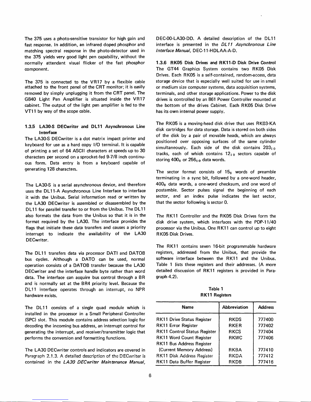
1.3.6 R
is
K05 Disk
The GT44 Graphics System contains two R
Drives. Each R
storage device
A detailed description of the
presented
in
the DL
11
DEC-11-HDLAA-A-D.
Drives
and R K11-D Disk
K05
is
a self-contained, random-access, data
that
is
especially
well
Asynchronous Line
Drive
Control
K05
suited for
use
in
DL
Disk
small
11
or medium size computer systems, data acquisition systems,
to
K05
the disk
Disk
Drive
terminals, and other storage applications. Power
is
drives
the
controlled by
bottom of
has its own internal power
an
861
Power Controller mounted at
the
drives Cabinet. Each R
supply.
1.3.5 LA30-S
DECwriter and
DL
11
Asynchronous Line
Interface
The LA30-S DECwriter
keyboard for
use
of printing a set of
is a dot
as
a hard copy I/O terminal.
64
ASCII
matrix impact printer and
characters at speeds up
It
is
capable
to
30
characters per second on a sprocket-fed 9-7/8 inch continu-
is
ous form. Data entry
from a keyboard capable of
generating 128 characters.
LA30-S
The
uses the D L 11-A Asynchronous
it
with the Unibus. Serial information read or written by
the
LA30 DECwriter
DL
11
also formats
format required by the
that
flags
interrupt
is
a serial asynchronous device, and therefore
Li
ne
is
for parallel transfer
the
data from
I nterface
assembled or disassembled by the
to
or from
the
the
Unibus so
to
Unibus. The
that
it
LA30. The interface provides the
initiate these data transfers and causes a priority
to
indicate the availability of
the
interface
DL
is
in
the
LA30
DECwriter.
DL
11
The
transfers data
via
processor
DATI
and
DATOB
bus cycles. Although a DATO can be used, normal
operation consists of a
and
DECwriter
the
DATOB
interface handle byte rather than word
data. The interface can acquire bus control through a
and
is
normally set
DL
11
interface operates through an interrupt, no
at
the B
transfer because the LA30
R4
priority
level.
Because the
BR
NPR
hardware exists.
The R K05
disk cartridges for data storage. Data
is
a moving-head disk drive
that
is
stored on both sides
of the disk by a pair of movable heads, which are always
positioned over opposing surfaces of the same
simultaneously. Each side of the disk contains 203
tracks, each of which contains 12
storing
4008 or 256
0
data words.
1
The sector format consists of 15
in
terminating
a sync bit, followed by a one-word header,
sectors capable of
10
words of preamble
8
4008 data words, a one-word checksum, and one word of
postamble. Sector pulses signal the beginning of each
sector, and an index pulse indicates the last sector,
that
the sector following
is
sector
O.
11
The
RK11
Controller and the RK05
Disk
disk drive system, which interfaces with the
processor
K05
R
The R
via
the
Unibus. One R
Disk
Drives.
K11
contains seven 16-bit programmable hardware
K11
can control up to eight
registers, addressed from the Unibus, that provide
software interface between
1 lists these registers and their addresses.
Table
detailed discussion of R K
the R K11
11
registers
and the Unibus.
is
provided
graph 4.2).
Table 1
RK11
Registers
uses
Drives
R K03-KA
cylinder
10
form the
PDP-11/40
the
(A
more
in
Para-
DL
11
The
installed
(SPC)
decoding
generating
performs
LA30 DECwriter controls and indicators are covered
The
Paragraph 2.1.3
contained
consists of a single quad module which
in
the processor
in
a Small Peripheral Controller
slot. This module contains address selection logic for
the
incoming bus address,
the
interrupt, and receiverltransmitter logic
the
conversion and formatting functions.
..
Il.
detailed description of
in
the
LA30
DECwriter Maintenance Manual,
an
interrupt control for
that
the D EC-v-vriter
in
is
K11
R
R
K11
RK11
R Kl1
R
K11
(Current Memory Address)
R
is
K11
RK11
Name Abbreviation
Drive Status Register
Error Register
Control Status Register
Word
Count Register
Bus
Address Register
Disk Address Register
Data Buffer Register
RKDS
RKER
RKCS
RKWC
RKBA
RKDA
RKDB
Address
777400
777402
777404
777406
777410
7774i2
777416
6
Page 14
Through software control,
the
RK11 can perform
four
control functions (Control Reset, Seek, Drive Reset, and
and
four
Write Lock)
Write Check,
transfer
R
KWC,
and
is
initiated by
a memory address
R KDA, and a code for
data transfer
Read Check).
the
CPU by storing a
"go"
RKCS. More detailed information
and
the
R K11-D Disk Drive Controller may be
RK05
Disk Drive Maintenance Manual (DEC-00-RK05-DB)
and
the
RKll-D
Controller Manual
1.3.7 BM792YB Bulk
The
BM792YB Bootstrap Loader
and
RKll-E
(DEC-11-HRKDA-B-D).
Storage Bootstrap Loader
matrix ROM, implemented on a
situated
program starting address
The
words
memory by
from location
assumed
The
in
the
PDP-11/40 mounting box. The BM792YB
is
773100.
actual
of
a disk
to
bootstrap
the
be
loader program, stored
is
transferred from
BM792-YB program.
0
of
the
disk and
operative
at
BM792-YB program jumps
satisfactory completion of
automatic
If
BM792-YB program,
The
bootstrap
starting
of
the
actual
error conditions occur during
the
program starts over again.
sequence
1.
of
operations used by
loader
is
as
follows:
It determines which device
by sensing an address
2.
It reads
256
words
starting with address
3.
The
loader
then
functions
For
example, a disk data
in
R KBA, a disk address
and direction (read
on
the
Moving Head Disk Drive
is
quad
size module, which
the
The
the
(Write, Read,
word
count
or
write) in
RK05 Disk Drive
found
in
a 32-word,
in
the
diode
first
disk into read-write
transfer
is
started
loaded routine
read-write memory location
to
the
transfer, so
bootstrap
set
0
of
stores
location 0
the
in
the
stored
the
the
loader program.
running
the
is
to
Switch Register.
from
disk.
256
after
that
there
of
bulk storage
be
read from
the
disk,
words
the
256
the
read-write memory sequential locations, starting with location
O.
in
in
is
O.
a
is
in
1.4
EQUIPMENT SPECIFICATIONS
Specifications
Graphics
PDP-11/40 Processor
1.4.1
to
Refer
coverage
1.4~2
VT11 Graphic Display Processor
Input
Power
+5 V at
+15
+22 V at
-22 V at
is
I nstruction Word Length
16
Raster Definition
10
Viewable Area
X =
Y =
Paper Size
12
Hardware Blink
Programmable
Hardware
8
Line
Frequency
Hardware programmable
Character
6 X 8
Characters/Line
73
of
the
components
System
of
are covered
the
PDP-11/40 Processor Handbook
in
the
PDP-11/40 specifications.
8 A
Vat
100 rnA
500
rnA
500
rnA
bits
bits
1024
raster unit (1777
1024
raster units (1777
)
8
)
8
bits
I ntensity Levels
Synchronization
Font
dot
matrix
(85 possible)
that
make up
the
GT44
following paragraphs.
for
detailed
4.
The
loader checks for errors and starts
program over if any errors occur.
5.
The
loader
then
jumps
location
bootstrap
A program listing for
provided
BM792YB
Only-Memory and
in
Appendix
bootstrap
0 for
automatic
loader program.
the
bulk storage
B.
For
a detailed description of
loader refer
MRll-DB
Bootstrap Loader Manual
(DEC-11-HBMD-D).
to
read-write memory
starting of
the
bootstrap
to
the
BM792
the
actual
loader
the
Read~
Number
of
Li
nes
42
Character
Set
96
ASCII - upper and lower case plus
31
specials
(GTeek letters, math symbols, etc.) (Refer
Appendix
A)
to
is
Control Characters
Line feed
Backspace
7
Page 15

Italics
Hardware programmable
Type
Line
Solid
long
dash
Short
dash
Dot-dash
Formats
Data
Character (2 char/word)
Short
Vector
long
Vector (2 words)
Point
(2 words)
Relative
Graphplot
Point
(1
XIV
word)
(1
word)
(1
word/pt)
Gain Change
From a fixed
gain change for each
Temperature
o
Relative Humidity
10
Linearity
Maximum deviation
of
straight line.
Deflection Method
Magnetic
Range
to
500 C (operating)
to
90% (noncondensing)
the
line length measured perpendicular
(700 diagonal deflection angle)
point
on
the
screen, less
±1
% line voltage variation
of
any
straight line will be < 1 %
than
to
a best-fit
±0.3%
DPU Instructions
Set
Graphic Modes
Jump
No
operation
load
Status
load
Status
1.4.3 VR17 CRT Display
Viewable Area
9.25
in. X
Brightness
>
25
fl
Contrast
Ratio
(NOP)
Register A
Register B
9.25
in.
(measured using a shrinking raster technique)
> 10:1
P39
±1 % of
Size
<
20
of
30
Type
doped
full scale
mils inside
fl,
full width
with I R
to
the
Phosphor
Pincushion
Spot
Monitor
best-fit line
usable screen area
at
half
maximum
at
a brightness
(FWHM)
Focus Method
I ectrostati c
E
High Voltage
10.5
kV
dc
nominal (voltage proportional
line voltage).
with a bleeder resistor.
Shielding
CRT
is
fully enclosed
Overload Protection
is
protected
Unit
thermal
current
against fault conditions.
1.4.4 375 Light Pen
length
5.0
Diameter
0.45
{1.143 em} (0.889 em)
Light Sensing
Phototransistor
cutouts.
limited. Phosphor
in. (12.7 cm)
in. (tapered
Supply
is
self-contained and equipped
in
a magnetic shield.
against fan failure
Power
to
0.35
supply
in.)
or
air blockage by
and amplifiers are
protection
is
to
input
provided
Jitter
<
±1/2
spot
diameter
Repeatability
<
±1
spot
diameter (repeatability
from
the
nominal location
of
any given spot)
is
the
deviation
Connector
Signal
8
Phone Plug
Amplification
G840
Light Pen Amplifier Module in V R 17 CRT
Display
Page 16

1.4.5 LA30 DECwriter
and
DL
11
Asynchronous Line
Interface
Printing
Speed
30 characters/second, asynchronous. 30 line
feeds/second, 300
ms
carriage return
Line Length
80 character positions
Character Spacing
10 characters/in.
ne
Spaci
Li
ng
6 lines/in.
Weight
110 Ib (50
DC
Power Supply
kg)
Self-contained (DEC Type H735)
Input
Power
115/230 Vac ±
10%
50/60 Hz
300W, maximum
Interface
DL
11-A * 20 rnA active current loop. Baud rate
selectable
1.4.6 RK05 Disk Drive
from
LA30
and
console.
RKll-D
Controller
Paper
9-7/8 in. wide continuous form, tractor driven {1/2
in. pitch X 9-3/8 in. wide X
0.150 in. diameter feed
holes}
Copies
One
part: 12
Two part: 12
to
20 Ib
to
13 Ib paper
7
to
7-1/2 Ib carbon
papers
Ribbon
4
mil Nylon, 1/2-in X 120 ft, medium inking
Typeface
5 X 7
dot
matrix
Printing Characters
64 upper
upper
case)
ASCII subset (lower
case
case
Keyboard Characters
97 or 128 (switch selectable)
Code
USASCII - 1968
Temperature
500 F (100 C)
- 1220 F (50°
C)
Humidity
5
to
90% (non-condensing)
Dimensions
(0.6
Depth - 24 in.
Width - 20-1/2 in. (0.5
Height -
31
1m)
m)
in. (0.79 m)
codes
print
R K05 Disk Drive
Storage Medium
Magnetic
Recording Density
Bit
in
Access
Bit
*
DL
Type -
Single disk magnetic cartridge
Disk Diameter - 14 in.
Heads
Number-
Density -
Tracks -
Two
and
Format
2200 bpi max.
406 (200 plus 3
spares
on
each
side
disk)
Cylinders - 203
(two
tracks
each)
Sectors (records) - 4872 (12 per revolution)/6496
(16 per revolution)
Capacities (unformatted)
Per
Disk - 25 million
Per
Inch - 2040 (max. at inner track)
Per
Cylinder
Per
Track - 57,600
Per
Sector - 4,800/3,844
Ti
mes
-115,200
Disk Rotation - 1500 ± 30 rpm
Average Latency -
Head Positioning -
(including settling time) -
20
ms
10
ms -for
(half rotation)
adjacent tracks
50
ms -average
ms -for
85
200 track
movement
Transfer
Transfer
Code - Double frequency, nonreturn-to-zero
recording
Transfer Rate - 1.44M bits per second
11
Registers and Interrupts are covered
in
Paragraph
4.2.
of
the
9
Page 17

Electrical Requirements
Voltage Power Starting
115/230
250
V A
Current
Vac @
50/60
Hz
- Power only: 1.8A
Start
spindle: 10A (for 2 seconds)
2.1.1
PDP-ll/40
The
PDP-l1/40
Operator's
following facilities:
STATUS INDICATORS
Console (Figure 2) provides
the
Environment
Ambient
Relative
(67°
to
Humidity - 8%
Temperature
73° C nominal)
Barometric Pressure -
Dimensions
and
Weight
Width - 19 in.
Depth Height Weight -
26-1/2
in.
10-1/2 in.
110
lb.
RK11-D Controller
Environmental Limits
Temperature
- 60°
(operating)
Relative Humidity -
condensation
(operating)
Vibration/Shock -
vibrations should
are transferring
data
Format
Drive
Format
-
1 disk cartridge/disk drive
203
cylinders/disk drive
2 disk surfaces/disk drive
2 tracks/cylinder
12
sectors/track
Data Word
Format16-bit
256
10
3072
10
614,400
data
word
=
4008 Data
=
60008 data
data words/surface
10
1,247,23210
Bit Density -
Recording Method -
Data Transfer Path - Unibus NPR
- 50°
to
110° F
to
80% (non-condensing)
30
± 3 mm
to
110° F
20
To
be
avoided while
to
80%
prevent
ambient
without
data
(operating)
words/sector
words/track
data
words/disk drive
approximately
Double frequency
hg
errors,
the
2200
extreme
disk drives
bpi
RUN
lights
when
the
the
processor
response,
WAIT
or
processor clock
is
waiting for an asynchronous peripheral
or
during a RESET instruction. It
HALT instruction.
is
running. It
PROCESSOR
lights
when
the
processor has
control
BUS
lights
when
the
UNIBUS
is
being used.
CONSOLE
lights
when in console
is
stopped
and
is
not
executing
mode
(manual operation). Machine
the
stored
USER
Lights when
the
CPU
is
executing program instn:Jctions
User mode.
VIRTUAL
Lights
when
the
ADDRESS Register display shows
16-bit virtual address. Not applicable
Management
option.
CONSOLE SWITCHES
POWER
OFF
ON
Power
Power
to
to
the
the
all console switches function
normally.
LOCK
to
Power
the
abied.
the
control switches are dis·
The
still functional.
Switch
Used
Register (Up =
to
manually load data
1)
(Down = 0)
or
an address into
processor.
Control Switches
is
off
is
on
during a
of
the
bus.
program.
without
processor
porcessor
processor
Memory
is
is
is
Switch Register
off.
on
on,
when
data
in
the
and
but
is
the
OPERATING CONTROLS AND INDICATORS
2.1
The
following paragraphs describe
System
controi
switches and indicators by
the
GT44 Graphics
component.
LOAD ADRS (depress
Transfers
contents
Address Register.
10
of
to
activate)
the
Switch Register
to
the
Bus
Page 18

Figure 2 PDP-11/40 Programmer's Console
The
resulting bus address
is
displayed
in
the
ADDRESS
Register, and provides an address for EXAM, DEP,
START.
program execution.
start
EXAM (depress
Causes
address
switch
The
location,
the
contents
to
be displayed
is
depressed again,
LOAD Address
To
restart a program
the
START
to
activate)
of
the
in
switch
the
is
not
modified during
at
the
is
activated.
location specified by
DATA Register. If
the
contents
the
of
previous
the
EXAM
the
sequential word location are displayed (bus address
incremented automatically).
the
next
lower even address
CONT (depress
Causes
the
at
which it had
CPU
is
in
to
processor
stopped.
the
RUN state. If
activate)
to
switch provides a restart
ENABLE/HALT ENABLE
If
an
word
continue
The
switch has
the
without
odd
address
is
will be displayed.
operation
program had
no
from
effect
stopped,
a System Reset.
Allows
the
perform
operations
program
control.
specified,
the
point
when
CPU
normal
under
and
bus
next
the
this
to
START
If
the
(depress
CPU
is
effect.
is
If
the
program had
causes a
then
System Reset signal
continue
ENABLE.
DEP (raise
Deposits
to
contents
specified by
again,
the
Switch Register
modified) are loaded into
address
specified,
is
incremented automatically.) If an
the
HALT
Causes
stop.
CONT switch will
now
of
a single instruc-
tion.
to
activate)
in
the
RUN
state,
the
START
stopped,
only if
depressing
to
the
ENABLE/HALT switch
occur;
the
the
activate)
of
the
Switch
the
bus address. If
next
lower even address word will be used.
Register into
the
contents
the
next
DEP switch
(which were
word
the
CPU
Depressing
cause
execution
switch has no
START
switch
program will
is
the
location
is
raised
probably
location. (Bus
odd
address
to
the
in
is
11
Page 19

DISPLAYS
ADDRESS Register
Displays
During a programmed HALT
display shows
the
address of data just examined
or
the
next
instruction address.
or
deposited.
WAIT instruction,
DATA Register
Displays
general register
instruction
data
just examined
operation,
RO
contents
the
or
deposited. During HALT,
are displayed. During single
processor
status
word
(PS)
displayed.
A more detailed description
and indicators may be found
of
PDP-ll/40
in
console switches
the
PDP-ll/40
System
Manual, DEC-l1-H40SA-A-D.
2.1.2
VR17
CRT
Display Monitor
The
VR17
front
panel contains:
ON-OFF/BRIGHTNESS Switch - Full
rotation shuts
supply
to
rotation increases
the
off
VR17
power. It also shuts
VTll
Graphic Display Processor. Clockwise
VR17
display brightness.
counter
clockwise
off
+22 V
POWER Indicator - Lights when operating power
present.
2.1.3 LA30 DECwriter
Aside from
indicators are
the
keyboard,
on
the
DECwriter console (Figure
the
following controls and
3).
the
MODE LOCAL LINE
2-Position
either local
BAUD RATE
150,300
110,
3-Position Switch - Selects
Baud rate clock frequencies for
110,
150,
More detailed operating information may be found
LA30
DECwriter Manual, DEC-00-LA30-DC.
is
2.1.4 R KOS
RK05
listed
in
Disk Drive
front
panel controls and indicators (Figure 4) are
Table 2.
2.1.5 Circuit Breakers and Fuses
The
user should be aware of
the
following circuit breakers
and fuses. If a circuit breaker trips upon being reset,
fuse blows upon replacement, there
system. Appropriate repair procedures should
followed.
2.1.S.1 Circuit Breakers - There
is
each 861 Power Controller panel.
located
controller
lower
cabinet,
at
the
in
the
front
panels.
and
a circuit breaker
bottom
of
drives cabinet
The
power controller
is
The
each GT44 cabinet. The power
is
accessed by removing
mounted
Supply panel, are accessible by pulling
processor
out
on
its slide mounts.
Switch
or
on-line operation.
and
300
- Selects
Baud.
in
or
is
a malfunction
in
then
one circuit breaker
power controllers are
in
the
processor
on
the
H742 Power
the
PDP-l1/40
the
the
if a
the
be
on
the
Control/l
ndicator
READY
LOCAL LINE FEED
Function
Lamp - Indicates power·up
printer electronics and
DECwriter
I ndicates an
is
READY for use.
interrupt
that
is
enabled
on
the
by keyboard electronics, if INT
bit
is
set by software.
Switch When depressed,
causes a local line feed
applied
code being
to
the
sent
printer
out
without
to
the
to
com-
be
puter. This control will also dis-
rupt
printing,
but
no characters
will be lost.
There
is
a circuit breaker on
the
Drive mounting box. These are accessible through
cabinet rear
A circuit breaker, located
door.
at
DECwriter, controls its ac power.
2.1.S.2 Fuses - There are three fuses
VR17
CRT
Display Monitor marked LINE, POS, and NEG.
The
POS
and/or
NEG fuses may blow,
power indicator lit.
a
3.1
GT44
OPERATING PROCEDURES
The
user should be familiar with all
indicators previously discussed before
procedures listed
in
the
following paragraphs.
12
rear
the
of
each R K05 Disk
the
rear
of
the
at
the
rear
yet
leave
the
the
controls and
attempting
drives
LA30
of
VR17
to
the
apply
Page 20

Figure 3 LA30 DECwriter Console
13
Page 21

Figure 4 R
K05
Table
Controls and Indicators
Controls and Indicators
2
Controls and
Indicators
RUN/LOAD
(rocker
WTPROT
(rocker switch -
spring-loaded off)
PWR
switx:h)
(indicator)
Description
RUN
position
a.
locks the drive front door
b.
accelerates the disk to
operating speed
c.
loads the read/write heads
ROY
d. lights the
LOAD
position
a.
unloads the read/write heads
b.
stops the disk rotation
c.
unlocks the drive front door
d. lights the
Do
not switch
position during a write
operation,
erroneous data being recorded.
Placing this momentary contact
switch
in
the
WT
WT
lights the
vents a write operation, and turns
off the FAULT indicator
Placing this switch
position a second time turns off the
WT
PROT indicator and allows a
write operation.
Lights when operating power
present.
PROT indicator, pre-
indicator
LOAD
indicator
CAUTION
to
the
as
this results
PROT position
if
in
the
WT
LOAD
in
lit.
PROT
is
ROY
ON
(indicator)
FAULT
(indicator)
WTPROT
(indicator)
II
14
Controls and
Indicators
(indicator)
CYL
Description
Lights when
a read/write/seek operation.
Lights when:
a.
b.
c.
Lights when:
a.
b.
Goes off when the
is
pressed or when the drive
cycled through a RUN/LOAD
I quence.
Lights when:
a.
b.
Goes off when the
is
pressed a second time or when
the drive
LOAD
the R K05
the drive
dition
a seek or restore operation
not being performed
the read/write heads are
itioned and settled.
erase or write current
sent without a
or,
the linear positioner transducer
lamp
the
or,
the operating system sends a
Write Protect command.
sequence.
is
in
the
WRITE
is
inoperative.
WT
WT
PROT switch
WT
is
recycled through a RUN/
is
ready for
READY
PROT switch
PROT switch
pos-
is
pre-
GATE
is
rese-
is
pressed
con-
is
Page 22

Tab!e 2 (Cant)
Controls
and
Indicators
10.
Ensure
and
on
that
LINE.
the
LA30
Controls
and
Indicators
--------+---------------
LOAD
(indicator)
WT
(indicator) Lights
RD (indicator)
3.1.1 GT44
Start
1. Determine
connected
2.
Turn
POWE
3.
Determine
lit.
4. T urn
ON-OFF/BRIGHTNESS switch
in
the
indicator light
on
at
Lights
accept
occurs.
Lights when a READ
occurs.
Up Procedures
that
to
an appropriate electrical
the
PDP-11/40 console key switch
R position.
that
RK05 POWER indicators are
the
clockwise direction.
just
this time.
Description
when
the
R K05
a disk cartridge.
when
a WR!TE
the
GT44
power
V R 1 7
below
fro
The
the
switch should be
is
ready
operation
operation
cords· are
outlet.
n t
3/4
of
red power
pan
the
to
to
the
e I
way
11. Place
12.
13. Place
14.
15. Depress
773100
is
the
starting address
in
the
read-only
Depress LOAD ADRS
the
PDP-11
/40.
777406
the
RK11 Disk Drive Controller Word
Register.
Place
the
ENABLE/HALT switch
most (ENABLE) position.
the
causes
the
RT-11 Monitor
core memory and run.
pond
by
printing
DECwriter:
RT-11
• Where
the
The
GT44
is
system disk
be made.
is
in
the
Switch
memory
in
the
SA. This
PDP-11/40
VXX
XX
Monitor.
now ready for use. If a
not
available, a
Register (SR). This
of
the
bootstrap
(ROM).
to
load
the
is
START
to
be loaded into
The
Monitor will res-
the
following on
is
the
version
copy
the
to
switch. This
should now
program
address into
address
number
of
Count
its upper-
the
of
backup
the
5. Press
switch
6.
Set
The
7.
Open
front
Ensure
8.
Ensure
off.
9.
Set
This starts disk rotation and loads
When
ROY indicator will light.
PDP-11/40 console ENABLE/HALT
down
to
halt
the
computer.
the
R K05 RUN/LOAD switch
LOAD indicator will light.
upper R K05 drive (System Device 0)
door
and load
that
it
that
the
the
RK05 RUN/LOAD switch
the
disk reaches operating speed,
the
System
is
properly seated and close
RK05
WT
to
LOAD.
Disk Cartridge.
door.
PROT indicator
to
RUN.
the
heads.
the
3.1.1.1 Duplicating
procedure
is
15
the
System
is
used for duplicating
the
1. With
set
Disk Drive (System Device 1)
2. When
door
that
3.
Set
for
4.
Ensure
Device 1
RT-11 Monitor running
the
RUN/LOAD switch
the
LOAD indicator lights, open drive
and insert a blank disk cartridge. Ensure
it
is
properly seated and close
the
RUN/LOAD switch
the
ROY indicator
that
the
WT
is
off.
Disk-The
the
system disk:
to
light.
PROT
on
of
the
lower R K05
to
LOAD.
the
to
RUN, and wait
indicator
following
the
GT44,
door.
of
System
Page 23

5. Depress
WT
PROT
switch
of
(the upper R K05 Disk Drive) once.
PROT indicator should light.
6.
On
the
DECwriter TYPE:
System
Device 0
Its WT
Response
R
PIP<CR>
RK1
*
*
:A=RKO:/S<CR>
RK1
:MON ITR.SYS=RKO:MON
*
3.1.2
GT44
Failure Procedures
The
following procedures should be followed in
the
GT44
fails
to
these checks,
the
user should notify
problem.
Do
not
fuses, unless
switch
breakers
upon
being replaced,
these
failure procedures and
Service Office.
Field
operate
equipment
reset
any
the
is
in
the
trip
upon
properly. If, after performing
operation
the
DEC Field Service Office
is
CAUTION
circuit breakers,
PDP·11/40
OFF
position. If circuit
being reset,
the
or
user should
notify
ITR.SYS/U<CR>
the
event
still unsatisfactory,
of
or
check
console
if fuses
power
blow
abort
the
DEC
the
Comment
4.
If, with
<CR>
the
This indicates
is
Verify
Power
the
PDP·l1/40
is
used
to
indicate
Carriage Return Key.
that
copying
completed.
that
all plugs connecting
to
each 861
Controller panel are properly seated.
console power switch in
the
POWER position, certain unit(s) shows no power indica·
tion:
1. Determine which 861 Power Controller
the
unit{s) gets its power from. (The R K05 and
PDP·11
in
VR17
obtain
their
respective cabinets.
power from
the
The
Display Monitor may obtain power
861
controller
DECwriter
and
from
either controller.)
with
the
If,
PDP·11/40
POWER position,
1. Check
Power Controllers are
the
seated in
that
present
Ensure
2.
861 Power
the
that
861 controller power cords are properly
the
at
that
console power switch
GT44
is
completely inoperative:
Indicators 1
the
wall receptacles; and b) verify
lit.
If
and 2 on
required power (115
the
wall receptacles.
the
circuit breaker (CB1)
Controller panel
position.
3. Ensure
that
switch on
the
R EMOTE
the
LOCAL ON·OFF·REMOTE
each
861
Power Controller panel
ON
position.
not:
in
the
the
861
a}
verify
that
or
230
ac)
is
on
each
is
in
the
ON
2. Check
3.
4.
that
Indicators 1
ding 861 Power Controller are
not:
a)
verify
that
properly seated in
and
230
ac)
Ensure
b) verify
is
present
that
that
the
and 2 on
the
controller power
the
the
required power (115
at
the
wall receptacle.
the
correspon·
wall receptacle
circuit breaker (CB1)
lit. If
cord
on
corresponding 861 Power Controller panel
the
ON position.
Ensure
that
the
LOCAL ON·OFF·REMOTE
switch
troller panel
on
the
corresponding 861 Power Con·
is
in
the
REMOTE
ON
position.
the
is
ON
is
or
in
ON
is
in
VSiify
Power
that
all plugs connecting
Controller panel are properly seated.
to
the
861
16
Page 24

Make
6.
the
each unpowered unit:
PDP-11/40
Pull
a.
mounts. Check
Supply
ensure
circuit breaker (CB1)
tion.
is
VR17
CRT
ao
V e r i f y t
ON-OFF/BRIGHTNESS switch
3/4
Verify
b.
into a switched
Controller.
Check
c.
V R 17. Replace if faulty.
following checks corresponding
out
the
PDP-11/40
indicator lamp
that
the
Verify
that
that
H742
the
on
the
H742 Power
is
lit. If it
Power
is
in
the
ON posi-
H742 Power
its slide
plugged into its power controller.
Display
Monitor
hat
the
V R 1 7
is
of
the
way in
the
clockwise direction.
that
the
VR17
is
properly plugged
the
LI
N E fuse
output
of
an 861 Power
at
the
rear
to
is
off,
Supply
Supply
rotated
of
the
4.1
GT44 PROGRAMMING CONCEPT
The
user
should
separate programmed processors: a PDP-11!40
(CPU)
and
programmed
execute its
All
instructions available
in
the
GT44.
components
The
DPU
communicates
by way
requests.
uses
code.
of
The
the
M F11-L memory for executing its own PDP-11
The
view
the
GT44
Graphics
System
as
computer
a display processor (DPU).
to
initiate
own
program.
Figure 1 shows
to
the
Unibus.
the
display, and
on
the
the
PDP-11/40 are executable
directly with
The
is
relationship
the
MFll-L
PDP-11/40
then
free
of
the
memory
non-processor requests (NPRs), i.e.,
PDP-11/40 CPU,
connected
in
parallel, also
DPU executes display instructions stored
two
to
GT44
DMA
in
semi-contiguous memory locations called display lists. A
memory
Program
CPU,
becomes
layout
Counter
via
the
the
starting address
example
(DPC)
Unibus,
MEMORY
ADDRESS 0
is
and
shown
in
~
in
the
DPU
the
data MOVed
of
the
display list.
____
..,..,..,..,..,..,~
Figure
5.
is
addressed by
.......
The
to
Display
the
the
DPC
is
If
there
2.
3.
LA30
DECwriter
1.
is
a.
b.
c.
R
a.
no
CRT
Verify
switch
Verify
pi
Ensure
at
Verify
in
K05
Verify
(CB
box
that
ugged
into
that
the
rear door)
that
the
LA30.
Disk Drives
that
1)
at
the
is
on.
display:
that
the
is
rotated
the
DECwriter
an 861 Power Controller.
the
circuit breaker (accessible
is
in
paper
is
the
R K05 circuit breaker
rear
of
VR17
ON-OFF/BRIGHTNESS
3/4
of
clockwise direction.
Check
the
two
fuses
at
the
marked POS and NEG. Replace if faulty.
With power off, verify
firmly seated
in
the
processor mounting box.
at
the
that
VR17
and
is
properly
the
ON
position.
properly positioned
the
drive mounting
the
way
in
the
rear
of
the
VR17,
the
scope cable
at
module
is
A320
Shown are
chained
closed
display
used
by
three" I ists"
together
file.
the
CPU
600
of
by
Display
The shaded memory
for
PDP-11
DISPLAY
INSTRUCTIONS
DISPLAY JUMP
DISPLAY
INSTRUCTIONS
DISPLAY JUMP
DISPLAY
INSTRUCTIONS
DISPLAY JUMP
display
instructions
Jump
code,data,buffer
Figure 5 Memory Layout Example
a
DATA
2000
a
DATA
5000
a
DATA
600
instructions
areas
and data
into one,
can be
registers,etc.
CP-0653
17
Page 25

4.2 IMPORTANT ADDRESSES
PDP-11/40
CPU General Registers
(only console addressable)
RO
777700
X
Status
Register (Read Only)
Contents:
X Position
Graphplot
Increment
772004
Bits (9:0)
(15:10)
R7
NOTE
All
addresses are Unibus addresses; Unibus address
bits (17:16) are
automatically set
bits (15:13) are 1s. Thus address
777700.
All
addresses are in octal.
to
177700 becomes
Switch Register (Read Only)
Display Register (Write Only)
CPU
Status
for
Register (Read/Write
bit
4 which
is
Read only)
except
Contents:
Carry
Bits
Overflow
Zero
Negative
Trace
Trap
Priority
Not
Used
Previous Mode
Current Mode
VT11 Graphic Display Processor
Display Program
Counter
(DPC)
( Read/Write)
If
the
DPU
has
to
write an
address resumes
Display
Status
stopped,
odd
number
the
Register (Read Only)
attemping
into this
display.
Contents:
Stop
Flag
Bits 15
Mode
Intensity
Light Pen Flag
Shift
Out
Edge Indicator
Italics
Blink
Spare (Not Used) 2
Line
777707
1, if address
0
1
2
3
4
(7:5)
(11
:8)
(13:12)
(15:14)
(14: 11)
(10:8)
7
6
5
4
3
(1
:0)
777570
777776
772000
772002
Y
Status
Register (Read Only)
Contents:
Y Position
Character Register
(Note: When
mode, and an illegal
the
program
Register can
to
a user routine
in
the
SH
code
is
interrupted.
then
be read
that
I FTED OUT character
(040
to
is
used
special character.)
Display Processor
Stop
Interrupt = 320
Light Pen
Time
Out
(All
display interrupts are requested
DL
11
- DECwriter Interface Addresses
Receiver
Status
Interrupt
Interrupt = 324
and
Shift
Out
Register (RCSR)
Vector Addresses
Interrupt = 330
Contents:
Not Used
Bits
RCVR ACT
(Receiver Active)
Not
Used (10:8)
RCVR DONE
(Receiver Done)
RCVR
INT
ENAB
(Receiver
Interrupt
Enable)
Not Used (5:0)
Receiver Buffer Register (RBUF)
Contents:
Not Used
Bits
Received Data Bits (7:0)
-+
The
Character
find
to
draw some
(15:12)
11
7
6
(15:8)
Bits (9:0)
(15: 10)
)
137
is
fetched,
8
the
dispatch
at
level BR4)
(Read Only)
(Read Only)
(Read/Write)
(Read Only)
772006
777560
777562
18
Page 26

Transmitter Status Register (XCSR)
Contents:
Not
Used
XMIT
RDY
(Transmitter Ready)
XMIT
INT
ENB
(Transmitter
Enable)
Not
Used
MAINT
Not
Used
Transmitter Buffer Register (XBU
Contents:
Not
Used
TRANSMITTER
BUFFER (7:0)
DECwriter I nterrupt Vector Addresses
(Interrupt
Keyboard
Printer
RKll-D
Drive Status Register
(Read Only)
Interrupt
(Maintenance)
DATA
requested at level BR4)
Interrupt 60
Interrupt
Disk Controller
(R
(15:8)
Bits
7
6
(5:3)
2
(1
F)
Bits (15:8)
64
KDS)
:0)
777564
(Read
Only)
(Read/Write)
( Read/Write)
777566
(Write
Only)
777400
Contents (Cont):
Data Late
Read
Timing Error
Non-Existent Disk
Non-Existent
Non-Existent Sector
Not
Used
Checksum Error
Write
Check 'Error
Control
Contents:
Error
Hard Error
Search
Not
Inhibit
Format
Not
Stop
Control Ready
Interrupt
Memory Extension
Function
Go
Word
Status Register
Complete
Used
RKBA
Increment
Used
On
Soft
Error
On
Count Register (RKWC)
(Read/Write)
.
Cylinder
(R
KCS)
Bit
Bit
15
14
13
12
11
10
9
8
7
6
(5:4)
(3:
1)
0
9
8
7
6
5
(4:2)
1
o
(Read
(Read
(Read Only)
( Read/Write)
( Read/Write)
( Read/Write)!
(Read
( Read/Write)
(Read/Write)
(Read/Write)
(Write
777404
Only)
Only)
Only)
Only)
777406
Contents:
Ident.
Drive
Drive Power Low
High Density Disk Drive
Drive Unsafe
Seek
Incomplete
Sector Counter OK
Drive Ready
Access
Ready
Write Protect Status
Sector
Counter = Sector Address
Sector
Counter
Error Register (RKER)
(Read
Only)
Contents:
Drive Error
Overrun
Write Violation
Seek
Error
Programming Error
Non-Existent Memory
Bit
Bits
15
14
13
12
11
10
(15:13)
12
11
10
9
8
7
6
5
4
(3:0)
777402
Bus
Current
( Read/Write)
Disk Address Register
Data Buffer Register (RKDB)
(Read
Disk Drive
(requested at
For additional information on RK11 registers, refer
Address Register
Contents:
Select
Drive
Cylinder
Surface
Sector Address
Only)
Address
Interrupt
level BR5)
Vector Address
(R
KDA)
(R
KBA)
Bits (15:13)
(12:5)
4
(3:0)
777410
777412
777416
220
to
R K11-D and R K11-E Moving Head Disk Drive Controller
Manual,
BM792 Bootstrap ROM
DEC-11-HR KDA-B-D.
Starting Address
773100
19
Page 27

4.3
PDP-11/40 INSTRUCTION SET
A detailed description of
presented
guide assumes
in
the
PDP-11/40 Processor Handbook. This
that
the
the
PDP-l1/40
reader
instruction set
is
familiar with
PDP-11/40 instruction set and its general operation.
the
is
Table 3
operation.
is
a list
of
suggested mnemonics for GT44
4.4
VT11 INSTRUCTION
The
display processor instruction set consists
instructions:
Register A,
breakdown,
Set
Graphic Mode,
and
Load
by
bit
position,
provides similar information for
accompany
the
instructions.
Status
SET
Jump,
No-Op, Load
Register
of
B.
Figure 6 shows
each instruction. Figure 7
the
data words
NOTE
The user should
positions indicated as spare
4.5
PROGRAMMING EXAMPLES
The
following programming examples are meant
the
user with a basic introduction
technique. They have been kept brief
points being illustrated
not
insert 1-bits
or
unused.
to
not
be lost as would be
into
GT44
in
order
larger, operational program examples were used.
Address Instruction/Data
of
five basic
Status
the
that
those
to
provide
programming
that
the
the
case if
Program Listing 1
4.5.1 Initializing
To
start
the
loads
the
Display (processor) Program
the
starting address (SA)
Pointer must also be initialized
DPU,
the
Display Processor
the
CPU
executes a
of
short
Counter
the
display file.
to
an address above
prevent a stack overflow if an interrupt occurs.
Program Listing 1 illustrates these
4.5.2
Display File
The
program
to
be drawn
500,500
address. Then
established and
drawn
the
last commands reload
•
8
after
in
Program Listing 2 causes a
with
the
lower left corner
Initially,
the
the
DPC
the
display parameters, e.g., intensity, are
the
mode set
Point
is
executed and,
starting address. This results
re-executed;
Mnemonic
the
CRT display
Comment
is
to
Point.
the
DPC
in
is
refreshed.
two
operations.
at
loaded with
The
four
to
conclude
with
the
the
display file being
program
that
(DPC) with
The
Stack
4008 to
2008 unit
box
screen location
the
starting
vectors are
the
file,
display file
1000
1002
1004
1006
1010
1012
Address
1000
1002
1004
1006
1010
1012
2000
012706
500
012737
2000
172000
00001
instructioniData
012706
500
012737
2000
172000
000001
117124
MOV
#500,
MOV
#SA, @ #DPC
WAIT
Program Listing 2
Mnemonic
. =
1000
MOV
#500,
MOV
#2000,
WAIT
. =
2000
POINT+INT4+LPOFF
+BLKOFF+LlNED
20
R6 Initialize
Stack Pointer
Load
with SA =
Wait (or
PDP-ll
R6
Initialize
Stack Pointer
@ #DPC
Load
with SA =
Wait
Point mode, intensity
4,
no light pen, no
blink, solid
the
the
DPC
2000
other
code)
Comment
the
the
DPC
2000
lines.
Page 28

Program Listing 2 (cont)
Address Instruction/Data
2002
2004
2006
2010
2012
2014
2016
2020
500
500
110000
40200
0
40000
200 200
60200
2022 0
2024
2026
40000
20200
2030 160000
2032
Note
that
since the parameters (intensity level, no blink,
line type) are specified
and
need not be re-specified
in
2000
in
the
Point instruction,
the
Long Vector instruction
(2006) because they will not change unless
the
500
500
LONGV
200+INTX
0
O+INTX
200+INTX+MINUS
0
O+INTX
200+MINUS
DJMP
2000
they
appropriate
enable bits are set. The enable bits also allow the user
change, for example,
this case, only
the
line
the
line type enable bit
type
but
not
the intensity.
is
changed,
not
the
intensity enable bit. This retention of current, not-to-be-
Mnemonic
changed,
storage space.
4.5.3
to
In
The
CPU
restarts
This occurs
Comment
Unintensified point
at
X = 500, Y = 500
Long Vector mode
f:::.
X = 200,
f:::.
Y = 0
intensified
f:::.
X = 0,
f:::.
Y = 200,
intensified
f:::.
X = - 200,
f:::.
Y =
0,
intensified
f:::.
X = 0,
f:::.
Y = -
200
intensified
Jump
to
start
of
display
file.
values, saves both execution time and memory
Application
Stop
interrupt provides close interaction between the
and
the
the
at
of
the
Stop
DPU.
The
program
display after
the
the end of each pass.
Interrupt
in
Program Listing 3
halt and interrupt sequence.
Address
1000
Instruction/Data
012706
1002 500
1004
1006
1010
1012
012737
2000
172000
000001
1014
320
322
400
012737
402
404
172000
406
2000
117124
776
400
200
01
02
Program Listing 3
Mnemonic Comment
· = 1000
MOV
#500,
Rf'
MOV
#2000,
@ #DPC Load
WAIT
BR.-2
·
=320
400
200
·
=400
MOV
#1,
@ #DPC
RTI
· =
2000
PO!NT+!NT4+LPOFF
+BLKOFF+LlNED
Initialize
the
Stack Pointer
the
DPC
with
SA =
2000
Wait for interrupt
Jump
back
one
instruction
DPU
sends
Stop
interrupt
Address
to
Stop
of
next instruction
be
executed after a
interrupt
Processor status
(BR
level
4)
the
Resume
display
Return from interrupt
Point mode, intensity
4,
no
solid
light pen,
lines.
no
blink,
21
Page 29

Program Listing 3 (cont)
Address Instruction/Data
2002
2004
2006
2010
110000
40200
2012
2014
40000
2016
2020
60200
2022
2024
2026
2030
2032
40000
20200
173400
160000
2034
After initializing
The
DPU
the
Stop
interrupt
Since
to
the
the
DPU,
the
CPU
waits for an interrupt.
executes
the
display file, eventually performing
with interrupt enabled. This causes a vectored
address
320
.
8
Stack Pointer was initialized
stores its processor status and program
5008 and
Once stored,
contents
takes
status.
interrupt handler and
476
respectively; it pushes
8
the
CPU goes
as
the
the
address
contents
of
the
of
location 3228
I n this example, location
the
CPU proceeds
to
location
interrupt routine. The
4008 is
The interrupt handler simply MOVes
ope
which
is
interpreted
DPU
resumes operation, it will fetch and interpret
instruction after stopping;
start
of
the
display file. The final instruction of
interrupt handler
restoring
the
computer
placing
the
CPU
interrupt, i.e., it pops
branch back
the
CPU
in
as
a Resume by
in
this case a DJMP, back
is
a Return from Interrupt (RTI),
to
the
status and location present before
two
words
one
instruction
a WAIT condition again.
Mnemonic Comment
500
500
500
500
LONGV
200+INTX
Unintensified point
at
Long Vector Mode
~
0 0 intensified
O+INTX
200 200
200+INTX+MI
0
0
O+INTX
200+MINUS
DSTOP
NUS
~
intensified
~
intensified
.6.
intensified
Enable STop interrupt,
Stop
2000
DJMP
2000
Jump
display file after
a Resume
4.6.1
Stop
and Sync, Microcoding
Stop
and
Sync
appear
However, selection of both conditions
Status
A instruction should be avoided. Priorities have been
to
500
the
,
8
counter
them
on
in
the
location
"stack".
3208 and uses its
as
its new processor
the
address of
to
that
location.
the
number 1
the
DPU.
the
to
As
to
CPU
CPU
the
the
the
next
the
built into
microcoding
the
VT11 hardware concerning
of
these bits. The rules are as follows:
Sync
1.
2.
and
Sync
will override
but
will resume
Stop
and Sync with
Setting
Sync
and
Stop
ditions,
and restart automatically
frequency.
rather randomly with respect
the
effect
the
off
the
stack. A
is
executed, thus
4.6.2 Display File Changes
Restarting
the
"catch"
inconsistent
a Running Display - Restarting the
DPU
is
running should
the
CPU
in
or
undetermined operation.
X = 500, Y =
500
X = 200,.6. Y = 0,
X = 0,.6. Y = 200,
X = -200,
X =
in
.6.
Y = 0
0,
~
Y = -200,
to
start
of
the
Load Status A instruction.
in
any given Load
the
action on
Stop
Stop.
The display will
in
with
sync with
Stop
the
the
line frequency.
Interrupt Enabled
Stop
Interrupt enabled
must be avoided. Under these con-
the
DPU
will stop, post an interrupt,
in
Since
the
of
this microcoding
sync with
Sync resume happens
to
is
the
the
interrupt,
undetermined.
DPU
be
the
middle
avoided. It
of
a bus operation causing
is
possible
the
stop
line
while
to
4.6 PROGRAMMING RESTRICTIONS
As
with any complex system, certain restrictions must be
observed by
expected.
be aware
the
user if trouble-free operation
In
the
case
of
the
VT11,
the
of
certain programming limitations so
hardware may be exercised more proficiently
violating hardware rules.
is
to
be
programmer should
that
the
without
It
is
recommended
that
the
DPU
be halted with a
instruction before restarting it again.
Modification
of
the
File - Dynamic modification
display file should be avoided when possible. Normally
file can be modified dynamically
HO'Never,
it
is
possible
to
cause piOblems when modifying
without
22
Stop
of
the
the
consequence.
Page 30

SET
GRAPHiC
MODE
i5
i4
10
I I
JUMP
NO-OP
~~[~~~}~
o
11 0 SET
RElATIVE
SPARE
BITS
9
-7
INTENSITY
VAlUE }
INTENSITY
INTENSITY
SET,
ENABLES
INTERRUPT
ENABLED,
SET,
ENABlES
ON,
O'BLINK OfF
BITS
1-0
LINE
TYPE
VALUE}
LINE
DASH
SHORT
DASH
DASH
CONTROL
FOR
JUMP--------'-
-------------------------'
WORDS
I
OF
FOR
DISPLAY
POINT
NTO
BIT 5 INTO
BIT
INTO
~II
WORD.
CORE
0111
"I"
ENABLES
3-BIT
OOO'MINIMUM
111 'MAXIMUM
WHEN
l'
L P
WHEN
I'BlINJ(
"1"ENABLES
2-BIT
OO'SOLID
01
'LONG
10'
1 I 'DOT
"I"
INDICATES
"OP
CODE"
SPARE
B'TS
16
81TS
(21K
"1"INDICATES CONTROLWORD
"OP
CODE"
8ITS--------------------------'
SPARE
III~
MODE
THE
INTENSITY
REGISTER
----------
L P
INTERRUPT
ENABLE
0'''10
l P
INTERRUPT
4 INTO BliNK
WORD
2ND I
NO
REGISTER
-----------------------"
THE
LINEREGISTERS--------------------'
---------
JUMP
14
15
~J~~\==========~)~\~~~~~~~~~~~~~~~~~==================:j
15
~============~============~
ADDRESS
__________
NO-OP
15
14
J
~
OPl:RATION
~
----------
------------------'
1100
t
REGISTER
_________________
11
10
I
II
10
ADDRESS
I )
-1
SPARE
---#r
SPARE
LOAD STAnJS REGISTER A
"I"ltOCATES
~~L
~::'~::
WHEN
SET,
l'
INTERRUPT
CFWlLL
NOT
WHEN
SET,
O'POINT
Of
I'PONT ~ LIGHT
WHEN
SET,
l'ITAlICS
NOT
USED-------------------------~
HAlTS
DPU
SPARE
LOAD STAnJS REGISTER B
'T'
..,,,,'"
"OP CODE"
SPARE
------------------
WHEN
SET,
SETS
THE
DISTANCE
Figure 6 ! nstruction
14
15
CONTIIOl
WORD~
~
~C;::T:~ASE~GlSTER~
ENABlES
BIT e INTO
STOP
II/OS
WHEN
INTERRUPT
ENABlES
BIT 6 INTO
lIGHT
PEN
INTERACTION
Pl:N
INTERACTION
ENABlES
BIT
FONT, O'NORMAL
AND
RESUMES
OON"""."",-.1
FOR
LOAD
ENABLES
BITS
BETWEEN
NTEllRUPT
DISPLAY
STOPS
WHEN
DISPLAY
STOPS
THE L P.
INTENSITY
Will
BE
Will
4 INTO ITAliCS
IN
STATUS
0-5
NOT
REGISTER
FONT
------------------'
SYNC
WITH
LINE
~I
_I:~I~I-~~·-I---I~:-I-II~-IO--~-~~-~-~~-~-~~
~'
B REGISTER-.---J . I
INTO
GRAPHp\'OT
POINTS
EXECUTED
\AJcrd
II
1110
REGISTER
INTENSIFIED
BE
FREQUENCY--------------~
10
tdJJ
t t
~I
HIT
REGISTER
INTENSIFIED
-------------'
, ' r
INCREMENT
REGISTER
IN
GRAPHPLOT--------------'
Functions
I 0
I
[J
23
Page 31

CHARACTER
15
14
6
1ST 7-BIT
ASC
o
11
DATA
Mode
FORMAT-
0000
SHORT
VECTOR MODE-
Mode
0001
o INDICATES A DATA
7 BIT
ASCll
SPARE------------------------------'
7
BI
T ASCII
o INDICATES A DATA
INTENSIFY
o INDICATES
MOVES
1 INDICATES
MOVES
6
BIT
o INDICATES
MOVES
COMPONENT MOVES
6
BIT
CODE
CODE
VECTOR
TO
THE RIGHT; }
.o.X
TO
THE LEFT
MAGNITUDE Y
.0. Y COMPONENT}
UP; 1 INDICATES .o.y
MAGNITUDE Y
WORD
-----------'
_____________________________
WORD
IF A 1
.0.
X COMPONENT)
COMPONENT J
-----'
COMPONENT---------'
DOWN
COMPONENT-----------------------'
12
____________
6 BITS
.0.
-1
CP-0582
765
+/-
X
----J
6 BITS.o.y
o
CP-0583
LONG VECTOR
DATA FORMAT-
0010
o INDICATES A DATA
INTENSIFY
o
INDICATES
MOVES
INDICATES
MOVES
SPARE-------------------'
10
BIT MAGNITUDE X
o INDICATES A
SPARE------------~
o INDICATES
MOVES
COMPONENT MOVES
SPARE---------------------~
10 BIT MAGNITUDE Y
VECTOR
TO
THE RIGHT; 1 .
.o.X
TO
THE
UP; 1 INDICATES
Figure 7 Data Word
IF A 1
.o.X
COMPONENT}
COMPONENT
LEFT
DATA
WORD
.o.y
COMPONENT}
WORD
COMPONENT------------------'
.o.y
DOWN
COMPONENT---------------------J
Formats
24
(Sheet 1
of
2)
10
10
BITS
.o.X
BITS.o.y
o
CPOS'!!
o
CP-0542
Page 32

POINT
DATA
10
o
BITS X
MODE-
Mode
0011
o INDICATES A DATA
INTENSIFY POINT IF A 1
SPARE----------------------~
10
BIT X COORDINATE-----------------'
o INDICATES A
SPARE--------------------~
10 BIT Y COORDINATE
WORD
DATA
WORD
---------------------'
----'
10
CP0543
o
BITS Y
CP-0544
GRAPHPLOT
Mode
0100
GRAPHPLOT
Mode 0101
RELATIVE
POINT MODE-
Mode 0110
x-
v-
o INDICATES A DATA
SPARE------------~
JO
BIT X (Y)
o INDICATES A
INTENSIFY POINT IF A
o INDICATES X COMPONENT}
MOVES
TO
INDICATES X
MOVES
6 BIT MAGNITUDE X COMPONENT
THE RIGHT; 1
TO
THE
WORD
COORDINATE-----------------------'
J5
DATA
WORD
1----'
COMPONENT
LEFT
__
-----~
o INDICATES Y COMPONENT MOVES
1 INDICATES Y COMPONENT
6 BIT MAGNITUDE Y
MOVES
COMPONENT---------------~
6 BITS
--'
UP; } __________
DOWN
o
10
BITS X
(Y)
CP-0545
7 6 5
to
X
+/-
-l
6 BITS toy
o
CP-0546
Figure 7 Data Word Formats (Sheet 2
25
of
2)
Page 33

Table 3
Recommended GT44 Mnemonics
Group
1
Mnemonic
CHAR
SHORTV
LONGV
POINT
GRAPHX
GRAPHY
RELATV
INTO
INT1
INT2
INT3
INT4
INT5
INT6
INT7 3600
LPOFF
LPON
BLKOFF
BLKON
= Value
100000
104000
110000
114000
120000
124000
130000
2000
2200
2400
2600
3000
3200
3400 Intensity 6
100
140
20
30
Function
Character Mode
Short Vector
Long Vector Mode
Point Mode
Graphplot X Mode
Graphplot Y Mode
Relative Point Mode
Intensity 0
Intensity
Intensity
Intensity
Intensity
Intensity
Intensity
Light
Pen
Light
Pen
Blink
Off
Blink
On
Mode
(Dimmest)
1
2
3
4
5
7 (Brightest)
Off
On
Group 2
Group 3
L1NEO
L1NEl
L1NE2
L1NE3
DJMP
DNOP
160000
164000
26
4
5
6
7
Solid Line
Long
Dash
Short
Dash
Dot
Dash
Display
Display No Operation
Jump
Page 34

Table 3 (Cont)
Recommended GT44 Mnemonics
Group 4
Group 5
Mnemonic
STATSA
DSTOP
SINON
SINOF
LPUTE
LPDARK
ITALO
ITAL
SYNC
STATSB 174000
INCR
= Value
170000
173400
1400
1000 Stop I
200
300
40
1 60
100
Function
Load Status A Instruction
Display Stop
Stop I nterrupt
Light
Light
Italics
Italics
4
Halt
and
Status B Instruction
Load
Set
Graphplot Increment
nterrupt
Pen H it
Pen
Hit
Off
On
Resume
and
On
Off
On
Off
Interrupt
in
Sync
Group 6
(Vector/Point Mode)
INTX
MAXX
MAXY
MINUSX
MINUSY
Group 7
(Short Vector Mode)
MAXSX
MAXSY
MISVX
MISVY
40000 Intensify Vector or Point
1777
1777
20000
20000
17600
77
20000 Negative!:'
100
Maximum
Maximum!:'
Negative
Negative
Maximum!:'
Maximum
Negative!:, Y
6.
X Component
Y Component
6.
X Component
6.
Y Component
X Component
6.
Y Component
X Component
Component
27
Page 35

2-word instructions such
the
OPU fetched
modified
order
correct
intended address. It
halted before modifying
exercised
modify
the
second
code
and
will
address, causing
in
selecting
the
file.
the
word,
take
as
a Oisplay
first part
the
the
modified second
the
OPU
is
recommended
the
display file and
the
sequence
Jump.
of
a OJMP while
OPU
will process
to
of
commands used
For example, if
the
the
word
branch
that
the
that
to
OPU be
CPU
OJMP
as a
a non-
care be
to
4.6.3 Non-Flicker Display
The
quality of
determined
controlled by internal adjustments (contrast, focus, etc.)
and
the
external BRIGHTNESS control
However, programming
better
image
of
the
display parameters controlled by
Mode instruction,
ming plays.
repetitive dimming
characters
relatively long program
the
beginning
recycles
than
decay (the image will
when
apparent.
the
and
tive,
(1/30
program.
Program
most
factors: vector magnitude
and
about
the
display
there
from
second)
time,
of
When
the
the
image displayed
by
many
factors. Primarily,
is
also instrumental
quality.
Another
on
the
the
1/30
next
is
reintensified before
is
no
a programming
The
selectable brightness feature,
is
one
example
is
the
control
and
brightening
screen. Flicker, in this case,
execution
of
the
display frame until
display
of
frame begins,
the
apparent
execution
as defined above, and where vectors make up
display,
is
repeated. If this
a second,
become
program
the
dimmer),
to
time
the
flicker. Consequently,
standpoint,
period when designing a display
is
primarily
or
length, and
on
the
the
display
on
the
front
in
producing
the
Set
of
the
role
that
of
image flicker,
of
all vectors and
is
caused
time, i.e.,
screen fluorescence will
the
is
less
image dims noticeably
the
the
time
and
then
point
where flicker
than
1/30
is
not
to
determined
the
time
the
exceed
number
screen
panel.
one
Graphic
program-
the
by
from
program
is
longer
brighten
second,
objec-
this
by
two
of
vectors in
greater
will be. Figure 8 shows
these
display frames ~ 32
third
ratio. If this
because
decoded -
period. However, this
the
is
by a
is
vectors
area for each vector length with
practical limit. If vector lengths vary,
the
account;
exceed
the
display frame.
the
number
two
factors,
factor
is
the
time
ratio increases, i.e., when a mode word
number
is
increased. This
total number
the
32
ms.
of
for
ms
also present:
is
a 1: 1 ratio,
mode
that
of
vectors;
of
aggregate must
The
longer
vectors
a flickerless display, defined here
word
must be
time
the
longer
the
allowable limits, considering
(about
each length must be
1/30
the
vector
then
fewer vectors are allowed
itself requires
subtracted
is
more efficiently used when
the
total number
is
shown in Figure 8
the
not
cause
4.7 ADVANCED PROGRAMMING TECHNIQUES
a
4.7.1
Subroutines
This programming
code
is
repeated a
a display file. It precludes
of
the
is
efficient use
display subroutines
Interrupt
that
where
subroutine
file. An example
below. It
subroutine
subroutine
routine
instruction (OSTOP) followed by an identifier
informs
to
go. Figure 9 shows an example of
stack.
method
number
in
of
available storage space. Writing effective
the
interrupt
can be repeatedly called by
of
is
assumed
stack. STKST
is
used when a section
of times during
the
memory and
is
accomplished
service routine
an
interrupt
that
register R5
is
need
service routine
the
starting location for
the
vectors
the
display frame
second). Note
word
to
mode
time
from
the
is
accompanied
of
allowable
as
the
top
line being
as
is
usually
the
to
store multiple copies
therefore
through
the
taken
frame
of
the
execution
makes more
use
of
what
how
main display
is
used for
the
time
the
to
a display
is
and
the
that
word
to
be
32
ms
shaded
the
case,
into
to
display
of
Stop
do
shown
the
the
as
a
or
Mnemonic
STPINT:
TST@OPC
BEQSTOPO
MOV
AOO
MOV
RTI
OPC,-(R5)
#2,@R5
@ OPC,OPC
Comment
Test
the
address DPC
If
it contains a valid non-zero address, go
the
next
instruction; if
current
Push
The
stack now contains
from
the
Move address
OPC, i.e., go
Exit
28
OPC
subroutine.
pointed
to
is
on
stack.
the
subroutine.
pointing
not
go
the
return address
to
by OPC into
to.
to
STOPO.
to
the
Page 36

Mnemonic
Comment
MAXIMUM
NUMBER
OF
VECTORS
PER
32
MS
FRAME
5000
4000
3000
2000
1000
900
800
700
600
500
400
STOPO:
TOP:
-
-
-
-
j
-
-
-
-
-
-
CMP R5,
BEQ TOP
MOV
STKST
(R5)+,DPC
RTI
MOV#START,DPC
RTI
ONE
MODE
PER
.J
WORD
VECTOR
I
ONE
,PER
VECTORS
Is
the
subroutine
Yes, go
pop
No,
to
display file.
Exit
Restart
MODE
WORD
GROUP
to
top
of
off a word
at
top
of
OF
stack
empty?
display file.
and
go
display file
there,
and
i.e.,
exit.
return
300
-
200
-
100~------~~------~--------~------~--------~------~--------~-------r---
Figure 8 Non-Flicker Display as Determined by
VECTOR
29
MAGNITUDE
Vector
200
8
Quantity
and
Magnitude
1000
S
17778
CP-0651
Page 37

MAIN
DISPLAY FILE
START:
DISPLAY
DSTOP
DSTOP
DISPLAY SUBROUTINE
AD1:
DISPLAY
DSTOP
POINT
x=o
Y=O
DSTOP
AD1
CODE
1
AD1
0
CODE
1
o
}
Co"
,"b'."Ii
Call subroutine at
Signals
the end
1
..
ot
of
AD1
AD1
again
the main
CP-0659
file
4.7.2 Light Pen Interaction
The
DPU
is
stopped when a light pen (LP)
during
the
display
light pen interrupts are permitted (bits
Graphic Mode word must
pen
interrupt
Priorities permitting,
interrupt service routine
LP
interrupt has access
can be read by specifying
Display
•
Addr =
word following
hit occurred.
The
•
DPU
lute number.
of
a vector, character,
both
be
true
function).
the
LP
hit interrupts
that
is
called
to
three
data
the
addresses indicated):
Program
172000.
X position
stopped, Addr = 172004. A 10-bit abso-
Points
to
the
data word on which
of
the
display at
Figure 9 Subroutining Example
"hit"
occurs
or
point, provided
5 and 6 of
to
enable
the
in
as
in
the
Counter
the
instruction/data
the
PDP·ll.
a result
DPU
(the data
the
time
the
Set
light
The
of
the
(DPC)
the
LP
the
The
•
The service routine can respond
restarting
•
•
Y position
DPU
stopped,
lute number.
the
display in one
Resume
at
continue. Program example:
Restart
at
new display program routine
gram example:
the
the
the
time of
the
time
of
the
Addr = 172006. A 10-bit abso-
of
two
display -
the
display -
of
the
interrupt
MOV
4.7.3 Special Characters
31
The
(Appendix
Shift
special characters
Out
A)
are addressed through use
(0168) and Shift
in
In
the
(0178).
display
to
ways:
the
interrupt
the
#SA,DPC.
VT11 display character set
at
the
the
LP
interrupt by
operation
MOV
operation
is
in
is
allowed
#1
in
abandoned and a
is
initiated. Pro-
of
ASCII codes
time
progress
,DPC.
progress
the
to
30
Page 38

When
the
DPU
detects
hardware enters
the
through 0378 are decoded
appendix contains a list
that
when
the
DPU
(0168) itself
returned
is
a legitimate printing character.
to
the
non-special character ASCII set (non-shift
mode) when Shift I n
the
Shift
In
code (0178) does
to
be displayed. If, when
detects a code
In/Time
~
040
Out
interrupt vector. This
special characters (codes
in
the
Shift
mode. The PDP-11 now has access
order
bits of
the
7-bit illegal code. These 6 bits could be
used, for example,
the
Shift mode.
as
of
VT11 character codes). Note,
is
in
the
Shift
is
decoded. Unlike
not
in
,
the
PDP-11
8
000
through
as
an index
character code
In
this mode, codes
special characters (the
mode,
cause a special character
the
Shift
is
interrupted by a
to
generated characters.
4.7.4 Edge Violations
An edge violation occurs if either
the
indicated for a relative display causes
outside
relative points, characters,
relative
edge flag
the
physical limits
type
displays.) I n
in
the
the
status word
of
the
CRT face. (Vectors,
and
graphplots are classified as
event
of
an edge violation,
is
set and
016
8
the
Shift
Out
The
DPU
the
Shift
Out
mode,
the
is
because only
) are
037
a table
X or Y coordinate
the
the
8
to
of
display
display
legal when
the
6 low
software
to
is
clipped
,
the
000
code
code,
DPU
Shift
the
go
the
(terminated)
not
take
wrap-around can occur.
counting only up
at
the
edge
of
place. However, there
The
to
4095
vector position exceeds this 12-bit limit,
is
flows
to
0 and wrap-around occurs. For example, if four
consecutive vectors with
.6
= 1) are read, only
only one
space.
exceed
coordinates
will appear
caused
counting
that
The
the
the
is
can be displayed within
other
i 2-bit fieid.
of.6
X =
on
the
display
performed
points are limited
the
the
three
vectors cause
10
and .6 Y =
left
of
to
wrap
in
a 12-bit circular fashion. Absolute
to
10-bit addressing.
4.8 GT44 SOFTWARE
Utilization
covered
in
RT-11
of
the
software supplied with
the
following manuals:
System
Reference Manual, DEC-11-0RUGA-
A-D
BASIC/RT-11 Language Reference Manual, DEC-11-
LBACA-A-D.
the
screen; wrap-around does
is
one exception
VT11 hardware
, i.e.,
12
10
bits. Therefore, if
same coordinates
first vector
is
the
the
if a fifth
0,
is
the
display;
displayed; it
count
vector, with
decoded,
the
in
is
capable of
the
count
(.6
X =
physical address
to
the
hardware has
around. This relative X and Y
the
GT44
which
the
over-
1023,
is
the
legally
the
vector
is
31
Page 39

APPENDIX
A
7 Bit
( octal)
000
001
002
003
004
005
006
007
010
011
012
013
014
015
016
017
020
021
022
023
024
025
026
027
030
031
032
033
034
035
036
037
040
041
042
043
ASCII
Representation
NUL
SOH
STX
ETX
EOT
ENQ
ACK
BEL
BS
HT
LF
VT
FF
CR
SO
SI
DLE
DC1
DC2
DC3
DC4
NAK
SYN
ETB
CAN
EM
SUM
ESC
FS
GS
RS
US
SP
!
#
Keyboard
CTRL@'
CTRLA
CTRL B
CTRLC
CTRLD
CTRLE
CTRLF
CTRLG
CTRLH
CTRL I
CTRL J
CTRLK
CTRLL
CTRL M
CTRLN
CTRLO
CTRLP
CTRLQ
CTRLR
CTRLS
CTRLT
CTRLU
CTRLV
CTRLW
CTRLX
CTRLY
CTRLZ
CTRL
CTRL \
CTRL]
CTRL
CTRLSPACE BAR
SHIFT 1
SHIFT 2
SHIFT 3
(TAB)
(LF)
(CR)
[(ALT)
......
CHARACTER
GT44 Printing GT44 Printing
When
Preceded
Shift-Out =
A
ex
cp
~
0
Ll
rv
"1
Backspace
Line Feed
Carriage Return
Space 1 character
!
#
(')
1/J
0
..
J1
£-
Shift
1T
II
n
a
T
€
~
-+
t
,!,
I
1
=1=
:::::::
V
0
In
CODES
By
016
A-1
Page 40

7 Bit
(octal)
ASCII
Representation
Keyboard
GT
44
Printing
GT44
Printing
When Preceded
Shift-Out =
By
016
044
045
046
047
050
051
052
053
054
055
056
057
060
061
062
063
064
065
066
067
070
071
072
073
074
075
076
077
100
101 A
102 B
103
104
105 E
106
107
110
III
112
113
114
115 M
116 N
117
120
121
122
123
124
- (minus)
4
<
=
>
(a'
C
D
G
J
K
0
P
Q
R
S
T
$
%
&
,
(
)
*
+
SHIFT
4
SHIFT
5
SHIFT
6 &
SHIFT
7
SHIFT
8 (
SHIFT
9
SHIFT:
SHIFT;
, ,
-
/
0
1
2
3
5
6 6 6
7
8
9
?
F
H
I
L
/
0 0
1
2
3 3
4
5 5
7
8
9 9
,
SHIFT,
SHIFT
SHIFT.
SHIFT
/
@
SHIFT
A
SHIFT
B
SHIFT
C
SHIFT
D D
SHIFT
E E
SHIFT
F F
SHIFT
G G
SHIFT
H
I
SHIFT I
SHIFT
J J
SHIFT
K
SHIFT
L
SHIFT
M M
SHIFT
N N
SHIFT
0
SHIFT
P P
SHIFT
Q
SHIFT
R R
SHIFT
S
SHIFT
T
(tii
C
!
0
Q
S
$
%
,
)
*
+
-
/
1
2
4
7
8
<
=
>
?
A
B
H
I
K
L
T
,
I
A-2
Page 41

7 Bit ASCII
( octal) Representation
Keyboard
GT44
Printing
GT44 Printing
When Preceded By
Shift-Out =
016
125
126
127
130
131
132
133
134
135
136
137
140
141
142
143
144
145
146
147
150
151
152
153
154
155
156
157
160
161
162
163
164
165
166
167
170
171
172
173
174
175
176
177
U
V
W
X
y
Z
[
\
]
A
a
b
c
d D
e
f
g G
h
j
k K
m
n
0 0
P
q
u
V
w
X
y
z
RUB
OUT
SHIFT U U
SHIFT V
SHIFTW
SHIFT X
SHIFT Y
SHIFT Z
[
\
]
1\
SHIFT
(9')
A
B
C
E
F
H
J
L I
M
N
P
Q
V
W
X
Y
Z
\
1\
a
b
c
d
c
f
a
b
h
j
k
m
n
0
P
q
R
S
s
T
U
V
W
X
Y
Z
SHIFT [
u
V
w
X
y
z
{
SHIFT \
SHIFT]
SHIFTA
R.O.
L
•
[
]
I
I
A-3
Page 42

APPENDIX
B
173100
173104
113106
173110
173114
173120
113122
113126
173130
173132
173134
173136
173140
173144
113146
173150
113152
173154
113156
BOOTSTRAP
I
0000013
13000131
013101
171570
000005-
010100
012710
177400
020027
171344
001007
012140
004002
005110
100316
0135740
1130363
1322020
~1274e
0001305
1135710
100376
005110
100154
105010
000137
000000
000.001
REGISTER
R0=%0
Rl=Xl
BEGIN:
STARTz
MOV
RESET
MOV
MOV
eMF
BNE
MOV
TST
BPL
TST
8PL
eMP
MOV
TSTB
8PL
TST
8MI
CLRB
JMP
.ENO
BM792-YB
LOADER
ASSIGNMENTS:
Rl"R0
#-256.,,(ClR0
START
'''002,,-CR0>
@k0
•
-2
-
(R0)
BEGIN
(R0)+,,(k0)+
15"
-
(R0)
@H0
.-2
@R0
BEGIN
@k0
~I0
BULK
PROGRAM
JREAD SWITCH REG
JFORcE
s
••••
;SET
lIS
INO.
JYES.
J
WA
JlS
J
NO.
JADJUST
INOW
.n~AIT
JERROR
JIF
JFOR
JGO
CLEAR
DEVICE
TO
IT
GO
MOVE
I T
FOR
WC
READ
DECTAPE?
TO
~TART
TAPE
ERROFd
IT ENDZONE?
TRY A
GA
POINTER
START
FOR
ACTUAL
DONE
ENCOUNTERED?
SO
START
DECTAPE"STOP
TO
ROUTINE
IF
256
IN
OVEH
STORAGE
LISTING
FOR
••••
kETRY
ADDRESS
WORDS
TO
FRONT
READ
TRAN~POkT
LOADED
BEGIN
START
000004R
0vH~040R
R0
=~000000
=
000062k
B-1
Ri
=%000001
Page 43

READER'S COMMENTS
GT44 User's Guide
DEC-II-HGT44-A-D
Your comments and suggestions will help us in
our
publications.
What
is
your
general reaction
written, etc.? Is
What features are most useful?
it
easy
to
to
this manual? In
use?
-------------------------------------------------------------
What faults do you find with the manual?
our
continuous
your
judgment
effort
to
improve the quality and usefulness
is
it
complete, accurate, well organized, well
of
Does this manual satisfy the need
it
Does
Would
Please describe
Name
Street
City
satisfy
you
___________
your
needs?
please indicate any factual errors
your
position.
__________________
you
think it was intended
you
_
Sta te
_______________________
Why?
_
have found.
Organization
to
satisfy?
__________________________________
_
Zip
or
Country
_
J
Page 44

- - - - - - - - - - - Fold Here - - - - - -
-.-
--
--
--
--
- - - - - - - -
BUSINESS REPLY MAIL
NO
POSTAGE STAMP NECESSARY
Postage win be paid by:
Digital Equipment Corporation
Technical Documentation Department
146 Main
Maynard, Massachusetts 01754
/
DoNotTear-FoldHereandStaple
IF
MAILED IN THE UNITED STATES
Street
- - - - - -
FIRST CLASS
PERMIT NO. 33
MAYNARD,
--
MASS.
 Loading...