

Digital Equipment DV11 User Manual
DV11
communications
multiplexer
user's
manual
DV11
communications
multiplexer
user's
manual
EK-OV11-0P-001
digital
equipment
corporation • maynard,
massachusetts
Copyright © 1976 by Digital Equipment Corporation
The material in this manual
is
for informational
purposes and is subject
to
change without notice.
Digital Equipment
Corporation assumes no respon-
sibility for any errors which may appear
in this
manual.
Printed in U.s.A.
This document
was
set
on
DIGITAL's DECset-8000
computerized typesetting system.
The following are trademarks
of
Digital Equipment
Corporation, Maynard, Massachusetts:
DEC
DECCOMM
DECsystem-l0
DECSYSTEM-20
DECtape
DECUS
DIGITAL
MASSBUS
PDP
RSTS
lYPESET-8
lYPESET-ll
UNIBUS
1st Edition, December 1976
CHAPTER
1
1.1
1.2
1.2.1
1.2.1.i
1.2.1.2
1.2.2
1.3
1.3.1
CHAPTER 2
2.1
2.1.1
2.1.2
2.1.3
2.1.4
2.1.4.1
2.1.4.2
2.1.4.3
2.1.5
2.2
2.3
2.3.1
2.4
2.4.1
2.4.2
2.4.3
2.4.4
2.5
CHAFfER 3
3.1
3.1.1
3.1.2
3.1.2.1
3.1.2.2
3.1.2.3
3.1.2.4
3.1.3
3.1.3.1
3.1.3.2
3.1.3.3
3.1.3.4
3.1.3.5
3.1.4
3.1.4.1
3.1.4.2
CONTENTS
INTRODUCTION
AND
GENERAL DESCRIPTION
PURPOSE
AND
SCOPE
...........
.
DVII
COMMUNICATIONS
MULTIPLEXER .
DVll
Overview
Block Diagram
Establishing the Data Link
DVll
Operation . .
Reference Documents
PHYSICAL DESCRIPTION
General Specifications
INSTALLA
nON
SITE PREPARATION
AND
PLANNING
Minimum Through Maximum Configurations .
Compatibility Considerations and Precautions
Interface Specifications and Signals . . . . .
Interrupt Priorities and Address Assignments
Interrupt Priorities
........
.
Interrupt Vector Address Assignment
Address Assignments
Environment
............
.
UNPACKING
AND
INSPECTION
....
.
INSTALLATION OF
BASIC
ASSEMBLIES
Unibus Cable Interconnections
....
MODULE
INSTALLATION
AND
CUSTOMIZING
Unibus and Interrupt Vector Address Assignments
Synchronous Parameter Selection
Resistance Checks
.....
Installation
of
Add-On
DVll
SYSTEM
CHECKOUT
.....
.
PROGRAMMING
PROGRAMMABLE
FACILITIES
AND
FUNCTIONS
Programmable Registers
Control Table . . . . . . .
Control Table Format
Receive
Control Byte
Transmit Control Byte
Control Byte Symmetry
Operations With Directly-Addressable Registers
Modem Setup and Control
Accessing Secondary Registers
Data Transfer Enabling
Interrupt Enabling and Response
Extended Memory Addressing
Protocol Processing
.......
.
BCC
Polynomial Selections
Processing Block Terminations
iii
Page
1-1
1~1
1-1
1-2
1-2
1-3
1-3
1-3
2-1
2-1
2-1
2-2
2-2
2-2
2-2
2-2
....
....
~-~
2-4
2-4
2-5
2-5
2-5
· 2-13
· 2-16
..
2-16
· 2-17
3-1
3-1
3-4
3-4
3-4
3-5
3-5
3-5
3-5
3-6
3-6
3-6
3-6
3-6
3-6
3-6
CONTENTS (Cont)
Page
3.1.4.3
3.1.4.4
3.1.4.5
3.1.4.6
3.1.4.7
3.1.5
3.1.5.1
3.1.5.2
3.2
3.2.1
3.2.2
3.2.3
3.2.4
3.2.5
3.2.6
3.2.7
3.2.8
3.2.9
3.3
3.3.1
3.3.2
3.3.3
3.3.4
3.3.5
3.3.6
3.3.7
3.3.8
3.3.9
3.3.10
3.3.11
3.3.12
3.3.13
3.3.14
3.3.15
3.3.16
3.4
3.5
3.5.1
3.5.2
3.6
3.6.1
3.6.2
3.6.3
3.6.4
3.6.4.1
3.6.4.2
3.6.5
3.6.5.1
3.6.5.2
Control Byte Inhibit
Sync Character Selection . . . . . . . . . . . . . . . . . . . 3-7
Sync/Mark
Stripping Received Syncs
Line Activity
Data Transfer Operations
Provision for Alternate Data Transmission Tables
Table
DIRECTLY-ADDRESSABLE
System Control Register (SCR) . . . . . . . . . . . . . . 3-8
Line Control Register (LCR)
Receiver Interrupt Character Register (RIC)
NPR
Status Register (NSR)
Reserved Register
Special
Secondary Register Selection Register (SRS)
Secondary Register Access Register (SAR)
Modem Control Registers . . . . . . . . . . . . . . . . . . . . . . . . . . . . . 3-24
INDIRECTLY ADDRESSABLE (SECONDARy) REGISTERS
Transmitter Principal Current Address
Transmitter
Transmitter Alternate Current Address
Transmitter Alternate Byte Count
Receiver Current Address
Receiver Byte Count
Transmitter Accumulated Block Check Character
Receiver Accumulated Block Check Character
Transmitter Control Table Base Address
Receiver Control Table
Line
Line
Transmitter Mode Bits
Receiver Mode Bits
Line Progress
Receiver Control Byte Holding
CONTROL BYTE
DVl1
Line Modem
DVl1
DATA
Originating and Answering Calls . . . . . . . . . . . . . . . . . . . . . . . . . . 3-42
Resynchronization During Reception . . . . . . . .
Termination
BISYNC Implementation
DDCMP Implementation
Functions Register
Protocol Parameters
State
INITIALIZATION . . . . . . . . . . . . .
Data Transfer
TRANSFER IMPLEMENTATION
Transmission Control
Reception Control . . . . . . . . . . . . . . . . . . . . . . . . 3-43
Transmission Control . . . . . . . . . . . . . .
Reception Control . . . . . . . . . . . . . . . . . . . . . . . . . . . . . 3-48
State Select . . . .
Snapshot . . . . . . . . . . . . . . . . . . . . . . . . 3-7
Size and Location . . . . . . . . . . . . . . . . . . . . . . . . . 3-8
.....
Principal Byte Count (000
(lOll)
...
(1101)
(1110)
FORMAT.
Set-Up . . . . . . . . . . . . . . . . . . . . . . . . . . 3-41
of
Transmission and Reception
...
....................
REGISTERS
..........
..
. . . . . . . . . . . . . . . . . . 3-20
(SFR)
(0100)
(0101)
Base
(1100) . . . . . . . . . .
..........
Setup.
............
Address
(1010)
. . . . . . . . . . . . . . . . . . . . . . . . .
....
(1111)
. . . . . . . . . . . . . . . . . . . . . . . . . . 3-39
...
....................
......
. . . . . . . . . . . . . . . . . . . 3-7
..
............
......................
............
..................
. . . . . . . . . . . . . . . . 3-15
. . . . . . . . . . . . . . . 3-20
....
.....
...............
(0000)
I)
..
. . . . . . . . . . . . . . 3-29
(0010)
(00
II)
.........
(I
(100
.......
. . . . . . . . . . . . .
. . . . . . . . . . . . . . . .
..
(0110)
(0111)
...............
(00)
1) . . . . . .
. . . . . . . . . .
.
..............
..............
.......................
..
...........
...........
. . . . . . . . . . . . . . 3-43
. . . . . . . . . . . . . . . . . . . . . . 3-47
. . . . . . . 3-20
. . . . . . . 3-24
. . . . . . . . . . . 3-29
.
..........
. . . . . . . 3-32
.
........
.
..........
....
,
. . . . .
. . . . . .
..
.
....
....
...
..
.....
.....
3-7
3-7
3-7
3-7
3-8
3-8
3-15
3-29
3-32
3-32
3-32
3-32
3-32
. 3-33
. . 3-33
..
3-33
..
3-33
..
3-33
..
3-33
3-33
3-33
3-41
3-41
3-41
. 3-42
. . 3-42
. . 3-43
3-47
iv
CONTENTS
(Cont)
APPENDIX A PDP-II MEMORY ORGANIZATION AND ADDRESSING CONVENTIONS
APPENDIX
B PROTOCOLS
FOR
BINARY SYNCHRONOUS COMMUNICATIONS
APPENDIX C GLOSSARY
OF
TERMS AND
ABBREvlA
nONS
Figure No.
1-1
1-2
2-1
2-2
2-3
2-4
2-5
2-6
2-7
3-1
3-2
3-3
3-4
3-5
3-6
3-7
3-8
Table No.
1-1
2-1
2-2
2-3
2-4
2-5
3-1
3-2
3-3
ILLUSTRATIONS
DVll
Overview Block Diagram
DV
11
Communications Multiplexer
DVll
Interconnection Diagram
Module
Utilization Diagram
Title
DVll
M7836 Module - Device Address Selection Switches
DVll
M7837 Module -
Interrupt
Vector Address Selection
Switches for
DVll
Data Handling Section
........
.
DVll
M7807 Module - Device Address Selection Jumpers
and
Interrupt
Vector Address Selection Jumpers for
DVll
Modem Control Unit
..
. . . . . . . . . . . . . . . . . .
Location
of
Sync Switches
on
M7839 Module
......
.
Distribution Panel and Test
Connector
Jumper
Configuration
Control Byte Address
Control Byte Formats
DV
11
Primary Registers
DVl1
Secondary Registers
BISYNC Transmission Flow Diagram
BISYNC Reception Flow Diagram .
DDCMP Transmission Flow Diagram
DDCMP Reception Flow Diagram
TABLES
Title
Reference Documents
EIA Electrical Specifications
Device Address
Switches
..
Vector Address Switches for Data Handling Section
Vector Address Jumpers for Modem Control Unit
Synchronous Parameter Selection Switches
Functions
of
DVII
Programmable Registers
System Control Register Bit Assignments
Line
Control Register Bit ASSignments
(For
Synchronous Line Cards)
.....
v
Page
Page
1-2
1-5
2-4
2-6
2-7
2-8
· 2-9
· 2-14
·
2-18
3-4
·
3-5
· 3-9
· 3-30
...
344
· 3-46
..
3-48
..
3-49
Page
1-4
2-3
· 2-10
· 2-11
·
2-12
· 2-15
3-2
3-12
· 3-14
Table No.
34
3-5
3-6
3-7
3-8
3-9
3-10
3-11
3-12
3-13
3-14
3-15
TABLIS
(Cont)
TItle
Line Control Register Bit ASSignments
(For
Asynchronous Line Cards)
Receive
Function
Interrupt
Conditions
(For
Synchronous Line Cards)
....
Receive
Function
Interrupt
Conditions
(For
Asynchronous Line Cards)
Transmit
Function
Interrupt Conditions
.....
Control Status Register Bit Assignments
Line
Status Register Bit Assignments
line
Protocol Parameters Secondary Register Bit Assignments
Line
State Secondary Register Bit ASSignments
Line Progress Secondary Register Bit Assignments
Control Byte Bit Assignments
......
.
Transparent Data Transmission
Control
Non-Transparent Data Transmission Control
vi
Page
·
3-16
· 3-21
·
3-22
· 3-24
·
3-25
· 3-28
· 3-34
·
3-35
· 3-37
·
340
·
345
·
3-45

INTRODUCTION AND GENERAL DESCRIPTION
1.1
PURPOSE
This manual
gramming information for
nications Multiplexer.
chapters plus appendices:
Chapter I provides an introduction and overall
functional and physical descriptions
DVII;
Chapter 2 contains site preparation, interfacing,
and
installation information;
Chapter 3 includes all information necessary for
operation
program;
Appendices contain reference data, communications introductory data,
glossary
The
reader unfamiliar with communication line protocols should read Appendix B before attempting
Chapters I and
Terms unique to the
their first appearance. However, should the reader
encounter a word
to the glossary provided in Appendix C before
proceeding.
1.2
MULTIPLEXER
The DV II
PDP-II
DVII
family
AND
SCOPE
is
intended
of
of
terms
3.
is
a communications multiplexer for
of
computers.
to
provide operational pro-
the
DVll
The
manual consists
the
DV
II
via
the
and
an extensive
and
abbreviations.
DVII
that
COMMUNICATIONS
are generally defined
is
not
fully understood, refer
By
means
of
the
Commu-
of
three
of
the
PD
P-II
at
the
DVII,
CHAPTER 1
8
or
16
serial data lines can be multiplexed directly to
PDP-II
The
that provides the rules
data transfers
of
Protocols require processing to
mitted and received characters in order to identify
and respond to control characters, (2) maintain a
record
tion sequences, and (3) compute the error checking
~ode
transmitted
functions, thus relieving
head. A Core Memory
PDP-II
processing
The control table
which form a one-to-one correspondence with each
cha~acter
1.2.1 D
Figure I-I
ing the principal functional units,
trol lines for the DV
primary functional subsystems, as indicated on the
block diagram: a Modem Control
Handling Section. The Modem Control
itors
directed
Section sequences
between the modems and the
tively, core memory).
core memory for bidirectional data transfer.
DVII
is
intended for use with a PDP-II-program
or
protocol which govern the
and
the generation
data link control
of
control and data transmission a nd recep-
(block check calculation) on each character
or
program,
of
transmitted
VII
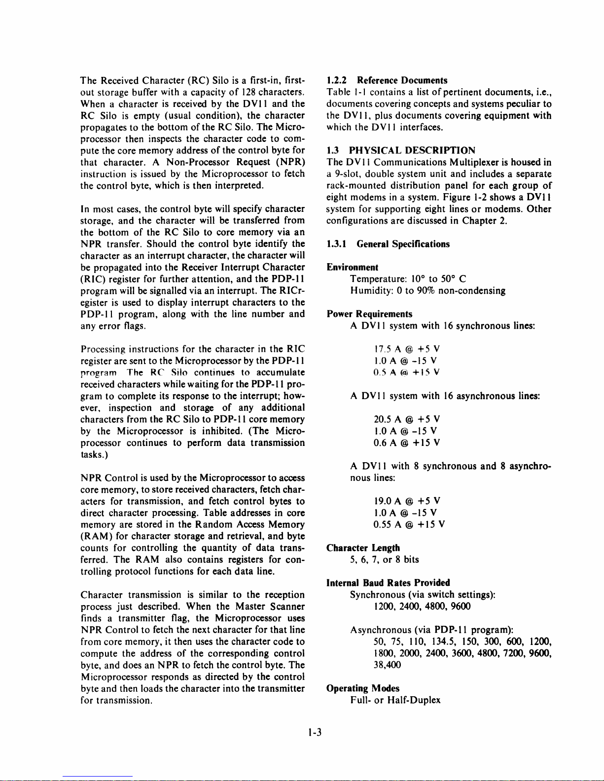
Ol'eniew Block Diagram
is a DV
and
controls operations
by
the PD
and
character codes.
received.
received
II
P-II
and
The
the
Control
is
used by the
and
is
comprised
or
received.
overview block diagram, show-
II.
The
program. The
synchronizes transfer
and
interpretation
(1) monitor trans-
DVII
performs these
processor
Table, set up by
transmitted characters.
DVII
of
the line modems as
PDP-II
of
DVII
to direct the
of
control bytes,
and
data
consists
Unit,
and
Unit mon-
Data
Unibus (effec-
this over-
and con-
of
a Data
Handling
of
the
two
data
I-I

MODEM CONTROL
INTERRUPT
SET-UP
MODEM
CONTROL
UNIT
MODEMS
I
DATA LINES
TO
---------------~-----
REMOTE
MODEMS
VI
::l
CD
DATA
HANDLING
Z ...------4
::l
SYNC
6FLAGS
Q.
MICRO-
RECEIVED
o
...------f
~------
..
CHARACTER
Q.
PROCESSOR SILO
......
----t
8
~-------"1
RECEIVER
INTERRUPT
CHARACTER
REGISTER
~--------~8~---------------------------------'
~--------~
8 t---------------------------------------------
11-
Z896
Figure I-I
DVII
Overview Block Diagram
1.2.1.1 Establishing the Data Link -
Data
transfer
is
enabled whenever
l.
An
operator
manually initiates a call
to
a
remote modem,
or
the
PDP-ll
program
dials the remote number via the
DNll
Automatic Calling Unit; when the data
link
is
established by the remote modem
answering the call, the
DVII
Modem
Control
U nit signals the
PDP-II
program
via
an
interrupt.
2.
In response to a
RING
signal from a
remote modem, the
DVII
Modem Con-
trol Unit interrupts the
PDP-II
program,
to
initiate an exchange
of
signals
that
establishes the
data
link.
1.2.1.2
DVII
Operation - With
the
data
link estab-
lished, the
PDP-II
program sets
up
the
DVII
Data
1-2
Handling Section to enable the
data
transfer between
the selected local modem
and
core memory.
The
serial/parallel interface
is
accomplished in the
receivers and transmitters. The receivers assemble
characters received from the serial data lines
and
set a
flag each time a character
is
assembled. The transmitters disassemble parallel characters for transmission on the serial
data
lines
and
set a flag each time
another character can
be
accepted for transmission.
The M aster Scanner cyclically enables the receivers
and
transmitters
to
route
their
flags
to
the
Microprocessor.
The
Microprocessor
is
controlled by a Read-Only
Memory
(ROM), which handles character transfers
and steps the Master Scanner.
Once started by the
PDP-II
program,
the
Microprocessor
runs
continuously.
The
Received
Character
(RC)
Silo
is
a first-in, first-
out
storage buffer with a capacity
of
128
characters.
When a character is received by the
DVII
and
the
RC Silo
is
empty (usual condition), the
character
propagates to the bottom
of
the
RC
Silo. The Micro-
processor then inspects the character code
to
com-
pute the core memory address
of
the control byte for
that
character. A Non-Processor Request
(NPR)
instruction
is
issued
by
the l\tficroprocessor
to
fetch
the control byte, which is then interpreted.
In most cases, the control byte will specify character
storage,
and
the character will be transferred from
the bottom
of
the
RC
Silo to core memory via
an
NPR
transfer. Should the control byte identify the
character as an interrupt character, the character will
be propagated into the Receiver
Interrupt
Character
(RIC) register for further attention,
and
the
PDP-ll
program will be signalled via an interrupt. The
RICr-
egister is used to display interrupt characters
to
the
PDP-II
program, along with the line
number
and
any
error
flags.
Processing instructions for the character in the
RIC
register are sent to the Microprocessor by the
PDP-II
program
The
RC Silo continues
to
accumulate
received characters while waiting for the
PO
P-II
pro-
gram
to
complete its response to the interrupt; how-
ever, inspection and storage
of
any additional
characters from the
RC
Silo
to
PDP-II
core memory
by the Microprocessor is inhibited.
(The
Micro-
processor continues
to
perform
data
transmission
tasks.)
NPR
Control
is
used by the Microprocessor
to
access
core memory, to store received characters, fetch
char-
acters for transmission,
and
fetch control bytes
to
direct character processing. Table addresses in core
memory are stored in the
Random
Access
Memory
(RAM)
for character storage
and
retrieval,
and
byte
counts for controlling the quantity
of
data
trans-
ferred.
The
RAM also contains registers for
con-
trolling protocol functions for each
data
line.
Character transmission
is
similar
to
the reception
process
just
described. When
the
Master
Scanner
finds a transmitter flag, the Microprocessor uses
N
PR Control
to
fetch the next character for
that
line
from core memory, it then uses the character
code
to
compute the address
of
the corresponding control
byte,
and
does an
NPR
to fetch the control byte. The
Microprocessor responds as directed by the control
byte and then loads the character into the transmitter
for transmission.
1-3
1.2.2 Reference Documents
Table
1-1
contains a list
of
pertinent documents, i.e.,
documents covering concepts
and
systems peculiar
to
the DV
II,
plus documents covering
equipment
with
which the
DVII
interfaces.
1.3
PHYSICAL
DESCRIPTION
The
DVII
Communications MUltiplexer
is
housed in
a 9-slot, double system unit
and
includeS a separate
rack-mounted distribution panel for each
group
of
eight modems in a system. Figure
1-2
shows a
DVII
system for supporting eight lines
or
modems.
Other
configurations
are
discussed in
Chapter
2.
1.3.1 General Specifications
Enfironment
Temperature: 10° to 50° C
Humidity: 0 to 90% non-condensing
Power Requirements
A
DVII
system with
16
synchronous lines:
t7.5A@+5V
1.0
A @
-15
V
O.5A@+15V
A
DVII
system with
16
asynchronous lines:
20.5 A @
+5
V
1.0A@-15V
0.6 A @
+15
V
A
DVII
with 8 synchronous
and
8 asynchro-
nous lines:
19.0 A @
+5
V
1.0 A @
-15
V
0.55 A @
+15
V
Character Length
5,
6, 7,
or
8 bits
Internal Baud Rates Profided
Synchronous (via switch settings):
1200, 2400, 4800, 9600
Asynchronous (via
PDP-II
program):
50,75,
110, 134.5,
150,300,600,
1200,
1800, 2000, 2400, 3600, 4800, 7200, 9600,
38,400
Operating Modes
Full-
or
Half-Duplex
Table
1-1
Reference Documents
Title
GENERAL
PDP-II Peripherals Handbook
PDP-II Instruction List
Logic Handbook
Introduction
Binary Synchronous
to
Minicomputer Networks
Communications
A Message-Oriented Protocol for
Interprocessor
Data Set
Communication
20lA
and
20lB
Interface
Specifications
Description
of
Discussion
overall system, addressing modes, and basic instruction set from a programming point
installation data.
Pocket-size list
and
bit
assignments. Includes ASCII codes and the bootstrap
of
instructions. List group names, functions, codes,
loader.
Presents functions and speCifications
and accessories used in
logic produced
Principles
Introduction
by
of
computer-based data communications technology.
to
Protocol (BISYNC
Introduction
to
PDP-II interfacing. Includes other types
DEC
but
not
used with the
IBM's Binary Synchronous Communications
or
BSC).
DEC's Digital Data Communication Message
Protocol (DDCMP).
Description
of
interface leads in synchronous modems.
of
view. Some interface and
of
the M-Series logic modules
PDP-II.
of
Set 201 C Interface Specification
Data
Data Set 208A Interface Specification
Data Set 208B Interface Specification
SOF1WARE
Paper-Tape Software Programming
Handbook
Interface Specification
Interface Specification
Interface Specification
of
Detailed discussion
the PDP-II software system used
dump, edit, assemble, and debug
is a discussion
of
input/output
programming and the floating-point
and math package.
to
load,
PDP-II programs. Also included
1-4
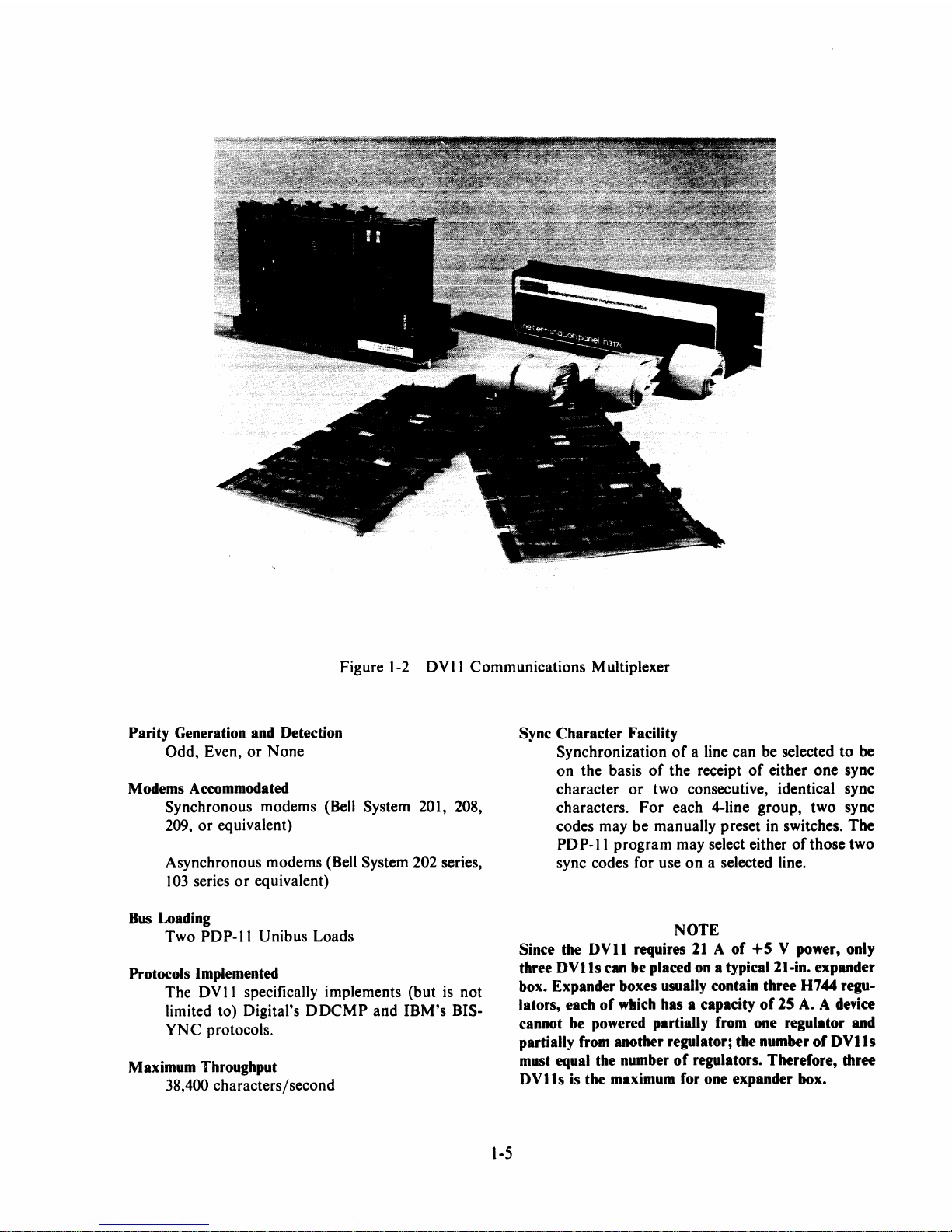
Figure 1-2
DVII
Communications
Multiplexer
Parity
Generation and Detection
Odd,
Even,
or
None
Modems Accommodated
Synchronous
modems
(Bell System 201, 208,
209,
or
equivalent)
Asynchronous
modems
(Bell System 202 series,
103
series
or
equivalent)
Bus Loading
Two
PDP-II
Unibus
Loads
Protocols Implemented
The
DV
II
specifically implements
(but
is
not
limited to) Digital's
DDCMP
and
IBM's
BIS-
YN
C protocols.
Maximum Throughput
38,400
characters/second
1-5
Sync
Character
Facility
Synchronization
of
a line
can
be selected
to
be
on
the basis
of
the
receipt
of
either
one
sync
character
or
two
consecutive, identical sync
characters.
For
each 4-line
group,
two
sync
codes
may
be
manually preset in switches.
The
PD
P-II
program
may select either
of
those
two
sync codes for use
on
a selected line.
NOTE
Since the
DVll
requires
21 A of
+5
V power, only
three
DVl1s
can"e
placed on a typicaI21-in. expander
box. Expander boxes
usually contain three H744 regu-
lators, each
of
which has a capacity
of
25 A. A device
cannot be powered partially from one regulator and
partially from another regulator; the number
of
DVl1s
must equal the number
of
regulators. Therefore, three
DVlls
is the maximum for one expander box.
This chapter provides information for interfacing,
installing, and testing the
DVII
Communications
Multiplexer. Interfacing considerations are discussed
in Section 2.1, Site Preparation and Planning.
Instal-
lation, customizing,
and
checkout procedures are dis-
cussed in Sections
2.2
through 2.7.
2.1
SITE
PREPARATION AND PLANNING
2.1.1 Minimum
Through Maximum Configurations
The
DVII
provides multiplexing capability to PDP-
i I core memory for up to
16
modems.
The
DVII
is
housed
in
a nine-slot, double system unit and includes one rack-mounted distribution panel for each
group
of
eight modems in a system. Five
of
the nine
slots are occupied by functions required in any
system configuration. The remaining four slots are occupied by four hex-printed circuit boards (M7839
or
M7833), designated as the line cards. Each line card
is
capable
of
supporting
data
transfers to and from four
modems.
The
M7839 line card supports synchronous
data
transfers while the M7833 supports asynchro-
nous data transfers (these line cards contain the
receivers
and
transmitters).
The 5-module unit common to all DV
11
con-
figurations
is
designated the
DVII-AA.
Two
of
the
M7839 module, plus one distribution panel and
associated cables, form an eight line synchronous unit
designated the DVII-BA. An eight line asynchronous
unit, the
DVll-BB,
is
generated by replacing the
M7839 modules in the
DVII-BA
unit with two
M7833 modules. Similarly, a mixture
of
one
of
each
line card forms a synchronous/asynchronous unit
designated the DVII-BC. The minimum
DVll
sys-
tem configuration consists
of
one
DVII-AA
unit plus
one line card option,
DVII-BA,
DVII-BB
or
DVll-
BC;
a maximum configuration consists
of
one
DVll-
AA
unit plus two line card options.
2-1
CHAPTER 2
INSTALLATION
2.1.2 Compatibility Considerations and Precautions
The
DVII
with synchronous line cards
is
directly
compatible with
Bell
synchronous modems 201, 208,
209,
or
equivalent.
It
is
also compatible with Bell
asynchronous modems
202 series,
103
series
or
equivalent when asynchronous line cards are used. The
DVII
provides internaal clock rates
of
1200,
2400,
4800, and 9600 baud at
0.005% accuracy for synchronous operation; modems operating at other rates
must supply their own clock signals.
It
is
recommended that modem-supplied clocking be used where
available.
The
DVII
is
compatible with all members
of
the
PD
P-II
family
of
computers.
PDP-II
standard software address allocations provide for the implementation
of
as many as four
DVlls
in a
PDP-II
system.
DVII
throughput rate, however, forms a more severe
limitation on the number
of
DVlls
in a system, as
will now be demonstrated.
A single
DVII
mUltiplexing
16
modems
at
9600
baud, each
in
full duplex mode,
is
capable
of
transferring 38,400 8-bit characters per second (1200 characters per line X
16
lines X 2 directions). Although this
is
well
within the capabilities
of
the
DVll,
on the
average, the
PDP-ll
is
provided with only
26
IlS
to
handle each character. Although most characters are
handled by
NPR
transfers, program and protocol
efficiencies still need to
be
relatively high to maintain
this rate; this would
be
for a single
DVII.
Some
76,800
NPR
cis
would be required,
or
about
10
per-
cent
of
Unibus capacity. With all lines operated in
DDCMP
mode (control byte fetch inhibited), 38,400
NPR
cis
would be required,
or
about 5 percent
of
Unibus capacity.
DVlls
should
be connected
ahead
of
all Massbus
devices
on
the Unibus
and
behind unbuffered
NPR
devices such as RK05s.
DVlls
have placement
requirements similar
to
those for
DQIls.
If
both
DQ
II
sand
DV
II s are
used, place
the
units with
the
highest
baud
rate
first.
If
all
DVlls
have
16
lines
at
a
9600
baud
rate, a maximum
of I DVII
can
be
con-
nected with
the
following exceptions:
a.
Two
DVlls
can
be
used
on a PDP-l
1/40,
PDP-I
1/45,
or
PDP-II/50
with
no
disks.
b.
Two
DVlls
can
be
used
on a PDP-II/70
with
no
Unibus
disks.
For
lower speed lines, the maximum
number
can
be
increased proportionally. (Example: a
PDP-II/40
with 2400
baud
rate
lines
can
use four
DVlls.)
A
maximum
of
four DV
lis
can
be
placed
on
any sys-
tem because
of
address space limitations; the limita-
tions
are
based
on
NPR
access.
Interrupt
performance depends
on
the
operating system, pro-
tocol,
and
buffer lengths.
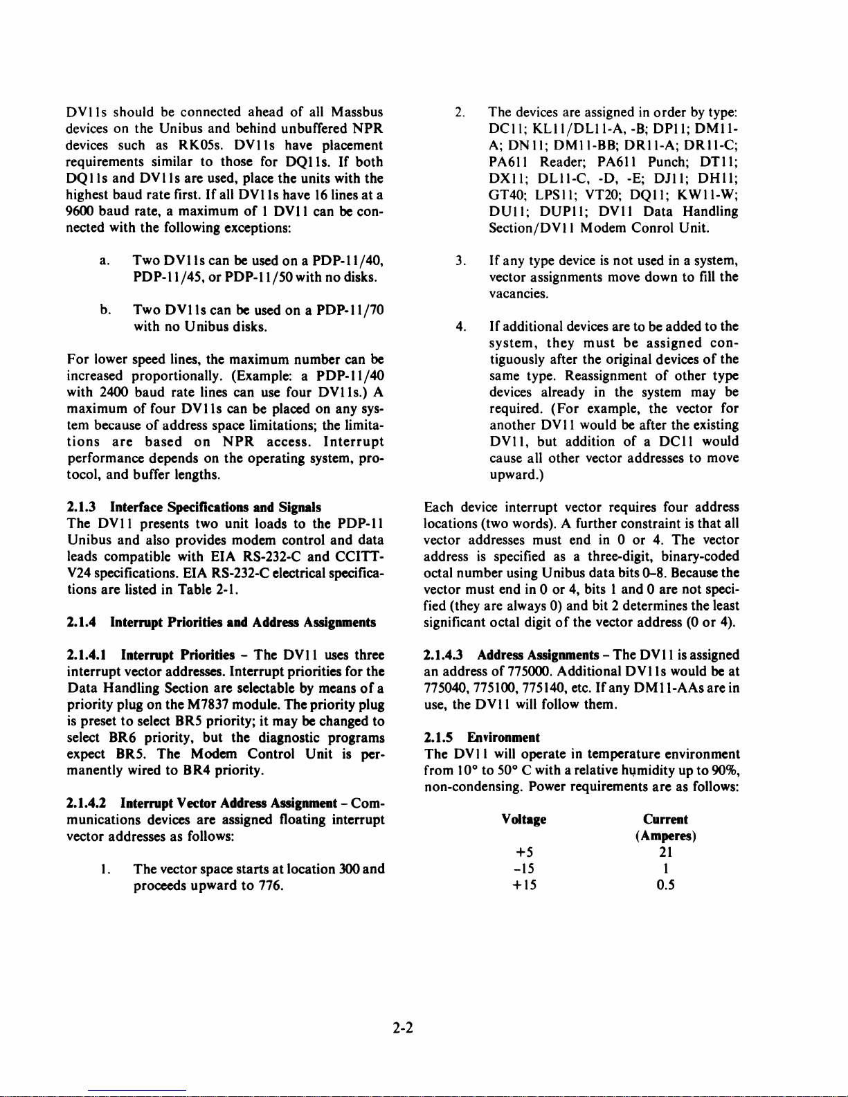
2.1.3 Interface Specifications and Signals
The
DVII
presents
two
unit loads to the
PDP-II
Unibus
and
also provides modem control
and
data
leads compatible with
EIA
RS-232-C
and
CCITT-
V24 specifications. EIA RS-232-C electrical specifica-
tions
are
listed in Table 2-1.
2.1.4 Interrupt Priorities and Address Assignments
2.1.4.1 Interrupt Priorities -
The
DVII
uses three
interrupt
vector addresses.
Interrupt
priorities for the
Data
Handling Section
are
selectable by means
of
a
priority plug
on
the
M7837 module.
The
priority plug
is preset
to
select BRS priority;
it
may
be
changed
to
select BR6 priority,
but
the diagnostic programs
expect BR5.
The
Modem
Control
Unit
is per-
manently wired
to
BR4
priority.
2.1.4.2 Interrupt Vector Address Assignment -
Com-
munications devices
are
assigned floating interrupt
vector addresses
as
follows:
I.
The
vector space
starts
at
location
300
and
proceeds
upward
to
776.
2-2
2.
The devices are assigned in
order
by type:
DCII;
KLII/DLII-A,
-B;
DPll;
DMII-
A;
DN
II;
DMII-BB;
DRII-A;
DRll-C;
PA611 Reader; PA611 Punch;
DTll;
DXII;
DLll-C,
-D,
-E;
DJII;
DHll;
GT40;
LPSII;
VT20;
DQII;
KWII-W;
DUll;
DUPII;
DVII
Data
Handling
Section/DVII
Modem
Conrol
Unit.
3.
If
any type device
is
not
used in a system,
vector assignments move down
to
fill
the
vacancies.
4.
I f additional devices are to be added
to
the
system,
they
must
be
assigned
con-
tiguously after
the
original devices
of
the
same type. Reassignment
of
other
type
devices already in
the
system may be
required.
(For
example, the vector for
another
DVII
would
be
after the existing
DV
II,
but
addition
of a DC
II
would
cause all
other
vector addresses
to
move
upward.)
Each device interrupt vector requires four address
locations (two words).
A further constraint is
that
all
vector addresses must end in 0
or
4.
The
vector
address
is
specified as a three-digit, binary-coded
octal
number
using Unibus
data
bits
0-8.
Because the
vector
must
end
in 0
or
4, bits I
and
0 are
not
speci-
fied (they
are
always 0) and bit 2 determines the least
significant octal digit
0 f the vector address (0
or
4).
2.1.4.3 Address Assignments -
The
DVII
is assigned
an
address
of
77S000. Additional
DVlls
would
be
at
77S04O,
77S100, 77S140, etc.
If
any
DMII-AAsarein
use, the
DVII
will follow them.
2.1.5 Environment
The
DVII
will operate in
temperature
environment
from 10°
to
50° C with a relative
h~midity
up
to
90%,
non-condensing. Power requirements
are
as follows:
Voltage
+S
-IS
+IS
Current
(Amperes)
21
1
O.S
Table
2-1
EIA Electrical Specifications
Driver
output
logic levels
with
3K
to
7K load
Driver
output
voltage with
open
cir-
cuit
Driver
output
impedance with power
off
Output
short
circuit current
Driver slew rate
Receiver
input
impedance
Receiver
input
vol tage
Receiver
output
with
open circuit
input
Receiver
output
with
+3 V
input
Receiver
output
with
-3 V input
+15
IZ/fl//T/I
+5
+3
0
S\\\\\\\\\
-3
~\~\\~~\\
-5
/7////////
-15
2-3
is
V>oh>
S V
-5 V
>01>
-15 V
IV
0
1
< 25 V
20>300
ohms
dv
dt
<
30
Vps
7KO>
R
in
>
3KO
±
15
V compatible
with
driver
Mark
Space
Mark
LOGIC
"0"=
SPACE - CONTROL ON
Noise margin
Transition region
Noise margin
LOGIC
"1"
= MARK = CONTROL
OFF
~.2
UNPACKING
AND
INSPECfION
\fter
unpacking, check
that
the
following
parts
are
)resent for
the
basic
DVII-AA
unit:
I
D-AD-7010834-0-0 Logic Assembly
I
M7807 Bus
Control
and
Mux
Board
I M7808
Modem
Control
Scan
and
M ux
Board
I M7836
ALU
and
Transfer
Bus
Board
I M7837
Unibus
Data
and
NPR
Control
Board
I M7838
ROM,
RAM,
and
Branch
Board
I
M920
Unibus
Connector
\Iso
check
that
the
following
parts
are
present
for
:ach line
card
option
ordered:
2 H8612 Line
Card
Test
Connectors
1 H 317C
Distribution
Panel
4 BC08R-15
Cables
I H325
Test
Connector
DVII-BA:
2 M7839 Sync
Mux
Line
Card
DVII-BB:
2 M7833 Async
Mux
Line
Card
DVII-BC:
I M7839 Sync
Mux
Line
Card;
M7833 Async
Mux
Line
Card
NOTE:
OUTPUT
CABLES
ARE BC...o5D-25
8 OUTPUT CABLES
H317C
DISTRIBUTION
PANEL
(FIRST 8 LINES)
H317C
DISTRIBUTION
PANEL
(SECOND I
LINES)
Install
all
BC08R
cables
with
smooth
side
toward
you
and
ribbed
side
toward
circuit
board.
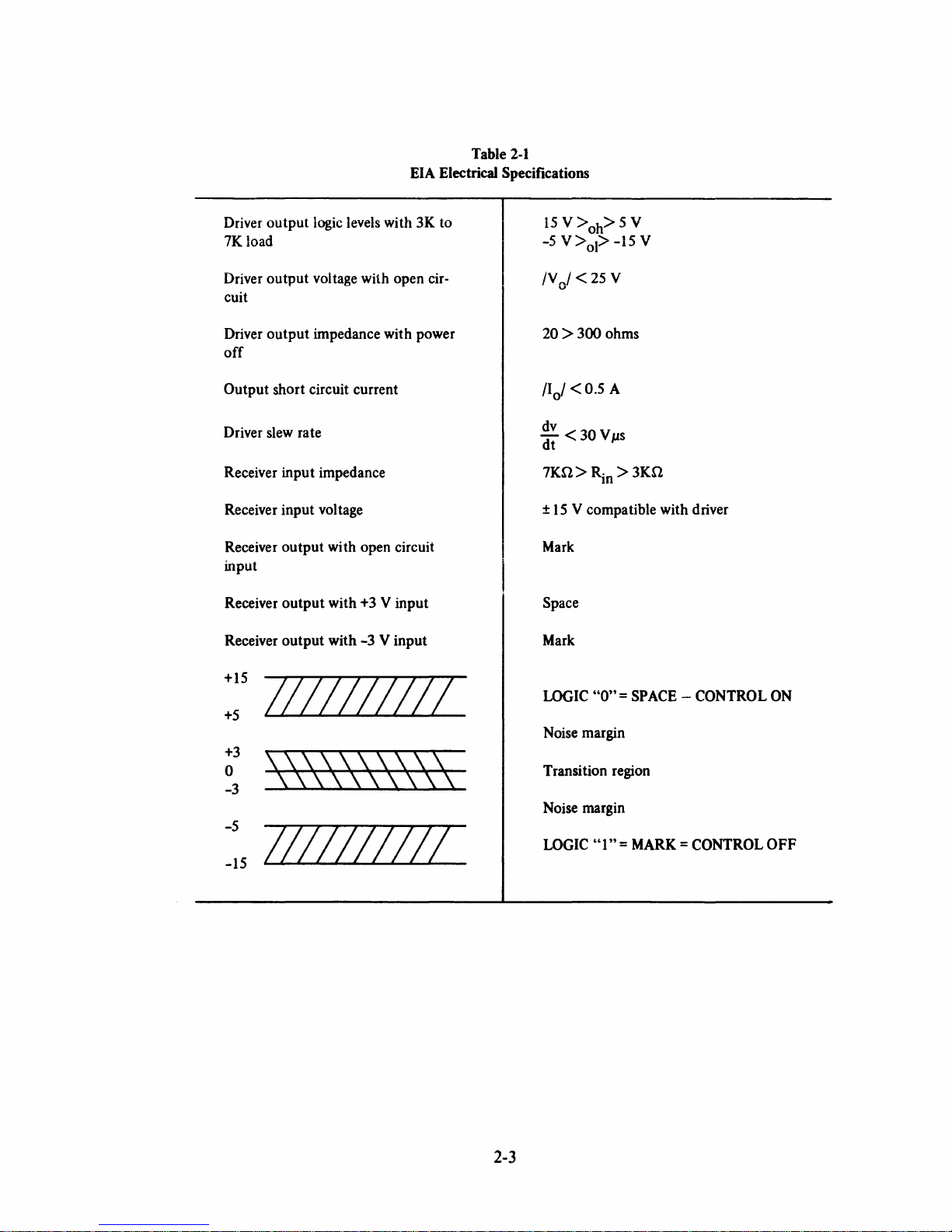
2.3
INSTALLATION
OF
BASIC
ASSEMBLIES
Drawing
D-
UA-
DV
11-0-0
shows
the
physical
arrangement
of
the wired backplane, distribution
panel(s)
and
cables in a typical installation.
Figure
2-
I
is
the
DV
11
interconnection schematic. Install
the
9-slot,
double
system unit in
the
expander
box
or
processor box as space
and
power
are
available.
With
power
off, test
the
resistances between all pins
of
the
power
harness
Mate-N-Lok
connector.
Only
pins
of
the
same
wire
color
should
be connected. Secure the
ground
wire
to
one
of
the
mounting
screws. Plug
in
the
Mate-N-Lok
connector
of
the
power
harness.
Apply
power
and
check for
proper
voltages
on
the
logic
pins
(not
the
cable) as follows:
Voltage
+5
± 0.25 V
-15
± 0.75 V
+15
± 0.75 V
Pin
CIA2
CIB2
CIUI
This
will
ensure
that
the
cable
and
the
Mate-N-Lok
connector
were correctly installed.
Turn
power
off.
(Note
that
the
DVII
is
not
yet
connected
to
the
Unibus,
nor
are
any modules installed.)
Install the distribution panel(s)
as
indicated in
Figure
2-1. Refer
to
Figure
2-7 for
the
proper
jumper
con-
figuration
of
the
distribution panel.
To
install
an
add-
on
DVIl,
see
Paragraph
2.4.4.
4
BCOIR
CABLES
4
BCOIR
CABLES
LINE
CARD SLOT 5
M
JI
LIN
LOT
PO
Pll
PROCESSOR
BOX
OR
BAIt
EXPANDER
BOX
THAT
CONTROL
THE
DVII
CONTROL
LOGIC WIRED
ASSY
D-AD-7010834
AC
POWER
CORD
TO
LINE
OR
PDP-l1
11-
2.50
Figure
2-1
DVII
Interconnection
Diagram
2-4
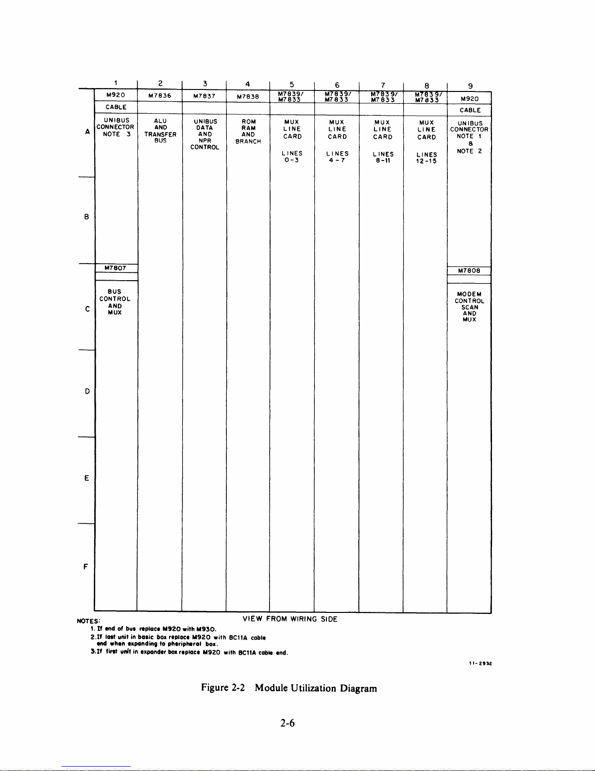
2.3.1 Unibus Cable Interconnections
The
DV II
is
shipped with
one
M920
Unibus
Connector (placed in slot 9 as shown in the module utilization program, Figure 2-2), which provides for
electrically connecting
the
unit
to
the
PDP-II
Unibus.
For
processor box installation where
the
unit
is
to
be electrically placed in mid-bus (i.e., somewhere
between
the
first
and
last devices
on
the
PDP-II
Unibus), the M920 from
the
next higher device
(closer to the processor)
on
the
bus is plugged
into
slot I
of
the
DVII,
and
the M920 in slot 9
of
the
DVII
is
plugged into slot I
of
the
next lower device
on
the
bus.
For
an end-of-bus installation
of
the
DVII,
proceed
as follows:
I. Remove the
M930
Unibus
Terminator
from the last slot
of
the
current
end-of-bus
device.
2.
Remove the M920 from slot 9
of
the
DVII
and place in slot I
of
the
DVII.
3.
Install
the
M930 (removed in step I) in
slot 9
of
the
DVll.
Unibus interconnections are
made
via
BCII-A
cables
where the DV
II
is
installed in
expander
box
or
is
physically the first
or
last unit in any box.
Cable
requirements in these cases
are
as described in Figure
2-2.
2.4
MODULE
INSTALLATION
AND
CUSTOMIZING
Figure 2-2
is
the
module utilization diagram. Set
the
address assignment
and
parameter
selection switches
as described in
Paragraphs
2.4.1
and
2.4.2 before
installing modules.
2.4.1
Unibus
and
Interrupt
Vector
Address
Assignments
The
Unibus
and
interrupt
vector addresses
for
the
DV
II
must be set manually before operating
the
2-5
DVII.
Two
Unibus addresses (also called device
addresses)
and
two
interrupt
vector addresses
are
provided on
the
D V
II
as follows:
1.
DVII
Data
Handling
Section address,
2.
DVII
~fCU
address,
3.
DV i i
Data
Handiing Section
interrupt
vector address,
4.
DVII
MCU
interrupt
vector address.
Because
the
DV
II
has ten registers directly address-
able by the
PDP-II
program, it must be assigned a
Unibus address
that
is
a mUltiple
of
32
(octal 40). All
DV
II
s in a
system
should
have
consecutive
addresses.
The
Unibus
addresses for
the
DVII
Data
Section
are
controlled by a rocker
DIP
switch package, located
on
module M7836,
and
by
jumper
straps
on
module
M7807 for the
DVII
MCU.
(Locations
of
all address
selection switches
and
jumpers
are shown in Figures
2-3
through
2-5.)
The
position
of
these switches deter-
mines bits 03-12
of
the
Unibus
address.
If a rocker
switch
is
set
to
ON
or a jumper
on
the M7807
board
is
in, an
address
bit
of
zero in the corresponding
bit
position serves
to
address
the
DVII
Data
Handling
Section.
DEC
standard
software requires
that
the
DVII
address
be
set as specified in
Paragraph
2.1.4.
Switch settings for device address selection
are
shown
in Table 2-2.
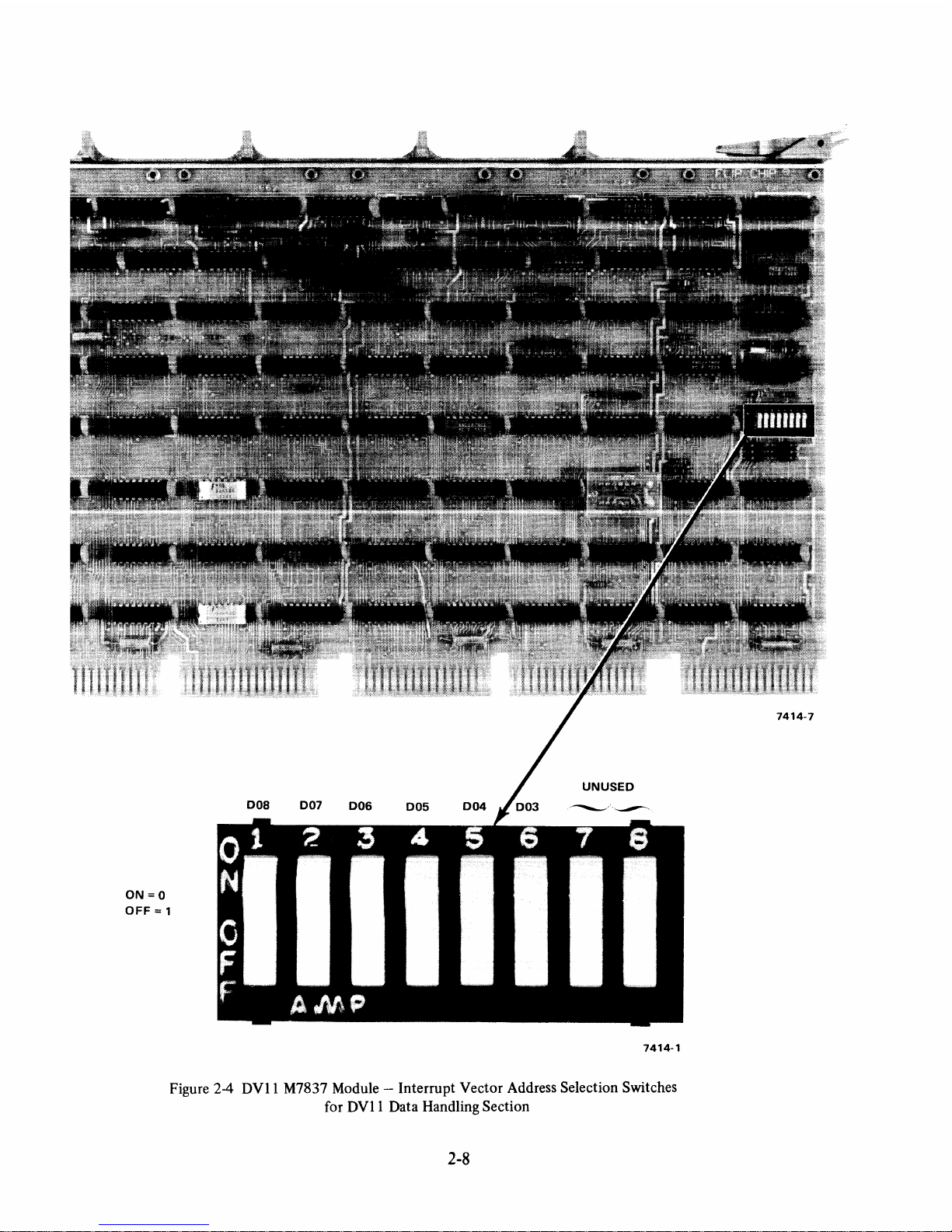
The
interrupt
vector address for
the
Data
Handling
Section
is
controlled by a
DIP
switch package
on
the
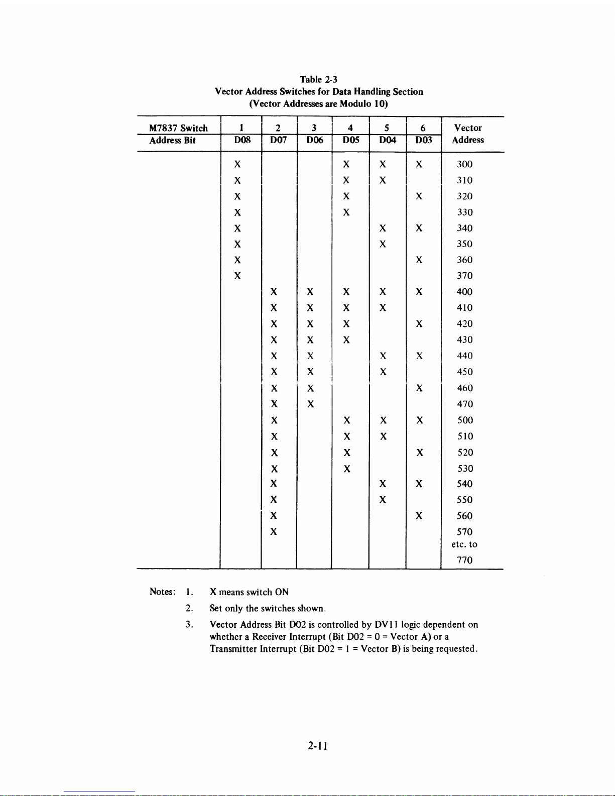
M7837 module, which selects vector address bits
08-03.
The
switches
should
be set
to
select
vector
addresses between 300
and
776. Switch settings
for
interrupt
vector address selection for
the
Data
Han-
dling Section
are
shown
in
Table
2-3. Vector address
selection for
the
Modem
Control
Unit
is
done
by
jumpers
on
the
M7807
module
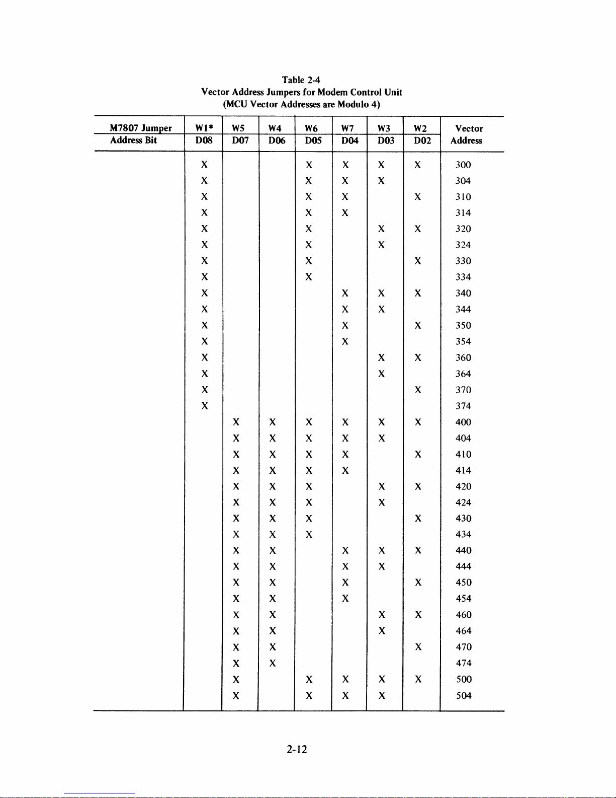
(Table 2-4).
CONNECTOR
A
-
B
1
M920
CABLE
UNIBUS
NOTE
3
M7836
TRANSFER
2
ALU
AND
BUS NPR
3
M7837
UNIBUS
DATA
AND
CONTROL
4
M7838
ROM
RAM
AND
BRANCH
5
M78391
M7833
MUX
LINE
CARD
LINES
0-3
6
~+~~r
MUX
LINE
CARD
LINES
4-7
7
~i~~~1
MUX
LINE
CARD
LINES
8-11
8
~~~~~I
MUX
LI
NE
CARD
LINES
12-15
9
M920
CABLE
UNIBUS
CONNECTOR
NOTE
S
NOTE
1
2
-
-
-
C
0
E
M7807
BUS
CONTROL
AND
MUX
M7808
MODEM
CONTROL
SCAN
AND
MUX
F
NOTES:
t.
If
end
of bus
replac.
2.If last unit in basic box
end
wh.n
3-.If
.xpanding
first unit in expander
M920 with M930.
replac.
to
M920
ph'riphtral
box
r.place
VIEW
FROM WIRING SIDE
with
BCllA
box.
M920 with
cable
BCttA
cable end.
Figure 2-2 Module Utilization Diagram
2-6
'1-
2932
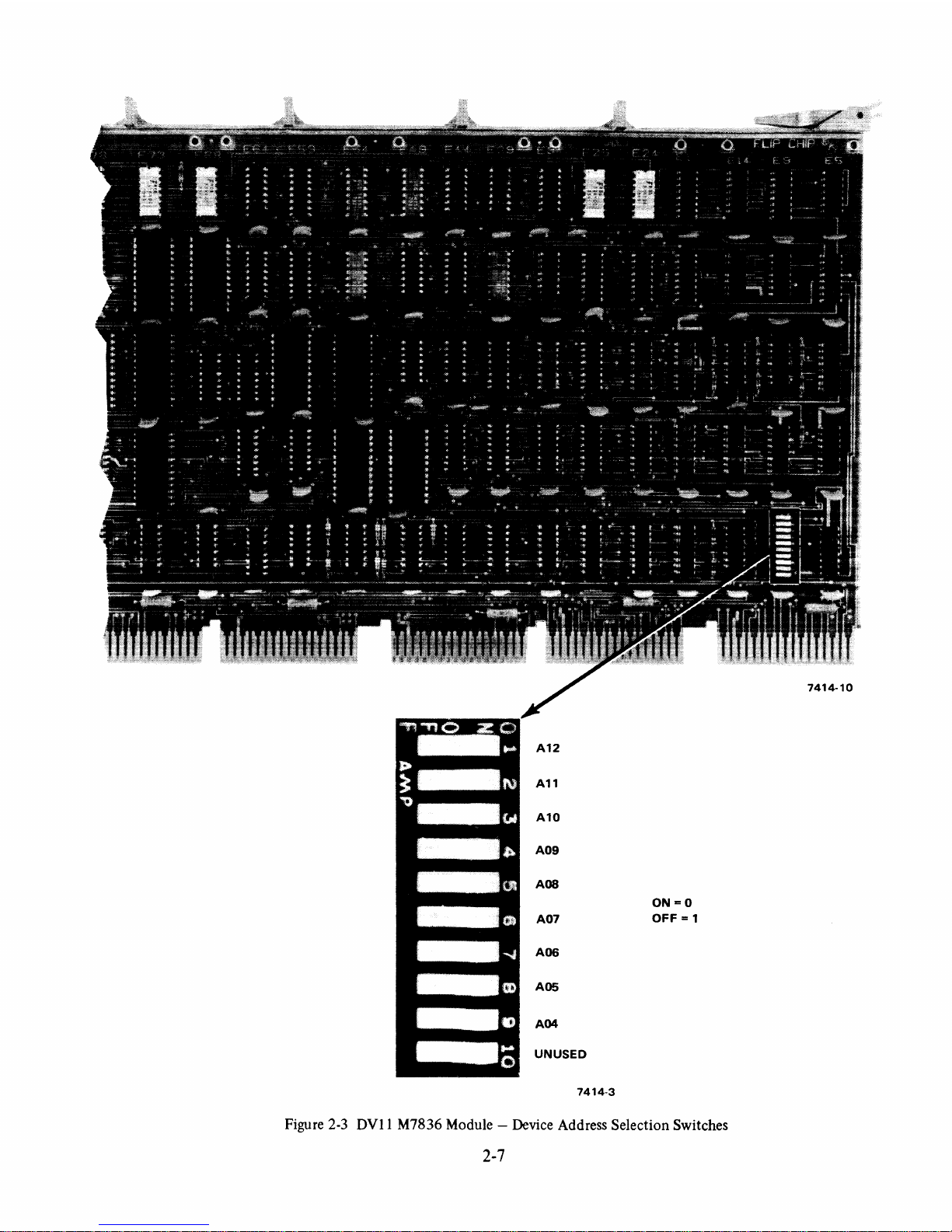
A12
A11
A10
A09
AOS
ON=O
A07
OFF
= 1
A06
A05
A04
UNUSED
7414-3
Figure 2-3
DVII
M7836 Module - Device Address Selection Switches
2-7
7414-1
Figure 2-4
DVll
M7837 Module - Interrupt Vector Address Selection Switches
for
DVll
Data Handling Section
2-8
INTERRUPT
VECTOR
ADDRESS
(002
-DOS)
Jumper
Bit
W1
DOS
W2
002
W3
003
W4
006
W5
007
W6
005
W7
004
Jumper
In
= 1
W18
W12
W17 W13
W5
W1
W2
W7
W3
W4
W6
Figure
2-5
DVII
M7807 Module - Device Address Selection Jumpers
and Interrupt Vector Address Selection Jumpers
for
DVII
Modem Control Unit
2-9
W16
Wl0
Wll
W9
W8
W15
W14
DEVICE
ADDRESS
(A03
-A12)
Jumper
Bit
W8
A12
W9
A09
Wl0
AOS
Wll
Al0
W12
A04
W13
A06
W14 A11
W15
A03
W16
A06
W17
A07
Jumper
In-O
7414-11
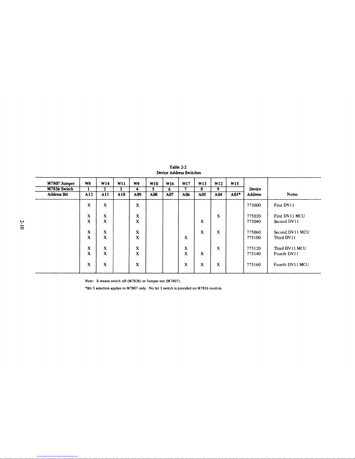
Table 2-2
Device Address Switches
M7807
Jumper
W8
WI4
Wll
W9
WIO WI6
WI7 WI3
WI2
WIS
M7836
Switch
I
2 3 4
S
6
7 8 9
Device
Address Bit
AI2
All
AIO A09
AOS
A07 A06
AOS
A04
A03*
Address
Notes
X X
X
775000
First
DV
11
X
X
X
X
775020
First DV
11
MeV
IV
I
X X
X
X
775040
Second
DVII
-
o
X X
X
X X
775060
Second DV
II
MeV
X X
X X
775100
Third
DVl1
X
X
X
X X
775120
Third
DVII
MeV
X X
X X X
775140
Fourth
DVII
X
X
X X X X
775160
Fourth
DVII
MeV
Note: X means switch
off
(M7836)
or
Jumper
out
(M7807).
*Bit 3 selection applies to M7807 only. No bit 3 switch
is
provided on M7836 module.
M7837 Switch
Address Bit
Notes:
1.
2.
3.
Table 2-3
Vector Address Switches for Data Handling Section
(Vector Addresses are Modulo
10)
1
2
3
4
5 6
D08 D07 D06 D05 D04
D03
x
X
X X
X
X X
X
X X
X
X
X
X
X
X
X
X
X
X
X X X X X
X X X
X
X X X
X
X X X
X X
X X
X
X
X
X X
X
X
X
X
X X X
X X X
X X
X
X
X
X
X
X
X
X
X
X
X
X means switch
ON
Set only the switches shown.
Vector
Address
300
310
320
330
340
350
360
370
400
410
420
430
440
450
460
470
500
510
520
530
540
550
560
570
etc. to
770
Vector Address
Bit
002
is
controlled by DVII logic dependent on
whether a Receiver Interrupt (Bit
002 = 0 = Vector
A)
or a
Transmitter Interrupt (Bit
002 = 1 = Vector
B)
is
being requested.
2-11
M7807 Jumper
Address Bit
Table 2-4
Vector Address Jumpers for Modem Control
Unit
(MCU
Vector Addresses are Modulo
4)
WI·
WS
W4
W6
W7
W3
DOS
007
006
DOS
004
003
X
X X
X
X
X X
X
X
X
X
X
X
X
X
X X
X
X X
X
X
X X
X X X
X
X X
X X
X
X
X
X
X
X
X
X
X
X
X
X
X
X X X X X
X X X X
X X X X
X
X X X
X X X
X
X X
X
X
X
X
X
X X
X
X
X
X
X
X
X
X
X
X
X
X
X X
X
X
X
X
X
X
X
X
X
X X
X
X
X X
2-12
W2
Vector
D02
Address
X 300
304
X
310
314
X 320
324
X 330
334
X
340
344
X
350
354
X 360
364
X 370
374
X 400
404
X
410
414
X
420
424
X 430
434
X
440
444
X 450
454
X 460
464
X
470
474
X 500
504
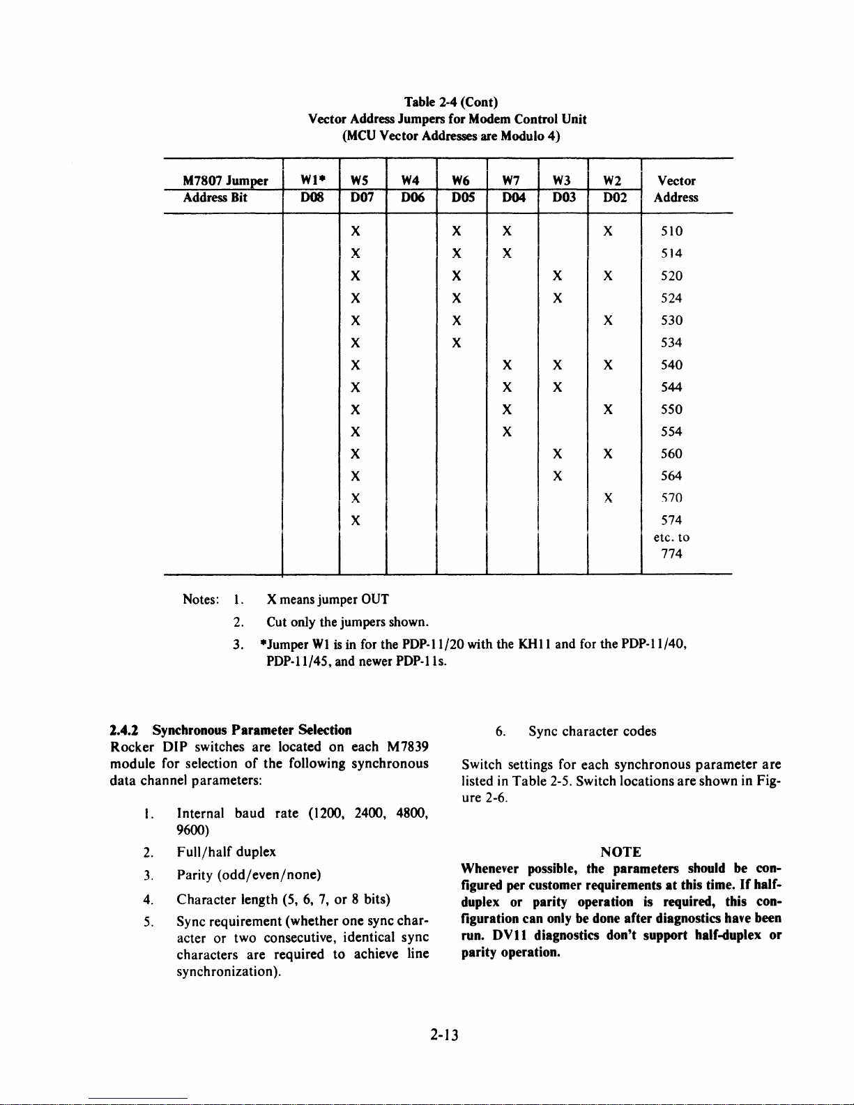
Table 2-4 (Cont)
Vector Address Jumpers for Modem Control
Unit
(MCU
Vector Addresses are Modulo
4)
M7807 Jumper
WI·
WS
W4
W6
W7
W3
W2
Vector
Address Bit
D08
D07 D06
DOS
D04
D03
D02
Address
X X X X
I
510
x X X
514
X
X
X X
520
X
X X
524
X X X
530
X
X
534
X X X
X
540
X
X X
544
X X
X
550
X X
554
X
X X
560
X
X
564
X
X
~70
X
574
etc. to
774
Notes:
1.
X means jumper
OUT
2.
Cut only the jumpers shown.
3.
·Jumper
WI
is in for the PDP-I 1/20 with the K.HII and for the PDP-I 1/40,
PDP-I 1/45, and newer PDP-lIs.
1.4.1
Synchronous
Parameter
Selection
Rocker
DIP
switches
are
located
on
each M7839
module
for selection
of
the
following
synchronous
data
channel parameters:
J.
Internal
baud
rate
(1200, 2400, 4800,
96(0)
2.
Full/half
duplex
3.
Parity
(odd/even/none)
4.
Character
length (5, 6,
7,
or
8 bits)
5. Sync
requirement
(whether
one
sync
char-
acter
or
two consecutive, identical
sync
characters
are
required
to
achieve line
synchronization).
2-13
6.
Sync
character
codes
Switch settings for
each
synchronous
parameter
are
listed in
Table
2-5.
Switch locations
are
shown
in Fig-
ure
2-6.
NOTE
Whenever possible, the
parameters
should be con-
figured per customer requirements
at
this time.
If
half-
duplex
or
parity operation is required, this con-
figuration
can
only be done
after
diagnostics have been
run.
DVll
diagnostics
don't
support half-duplex
or
parity operation.
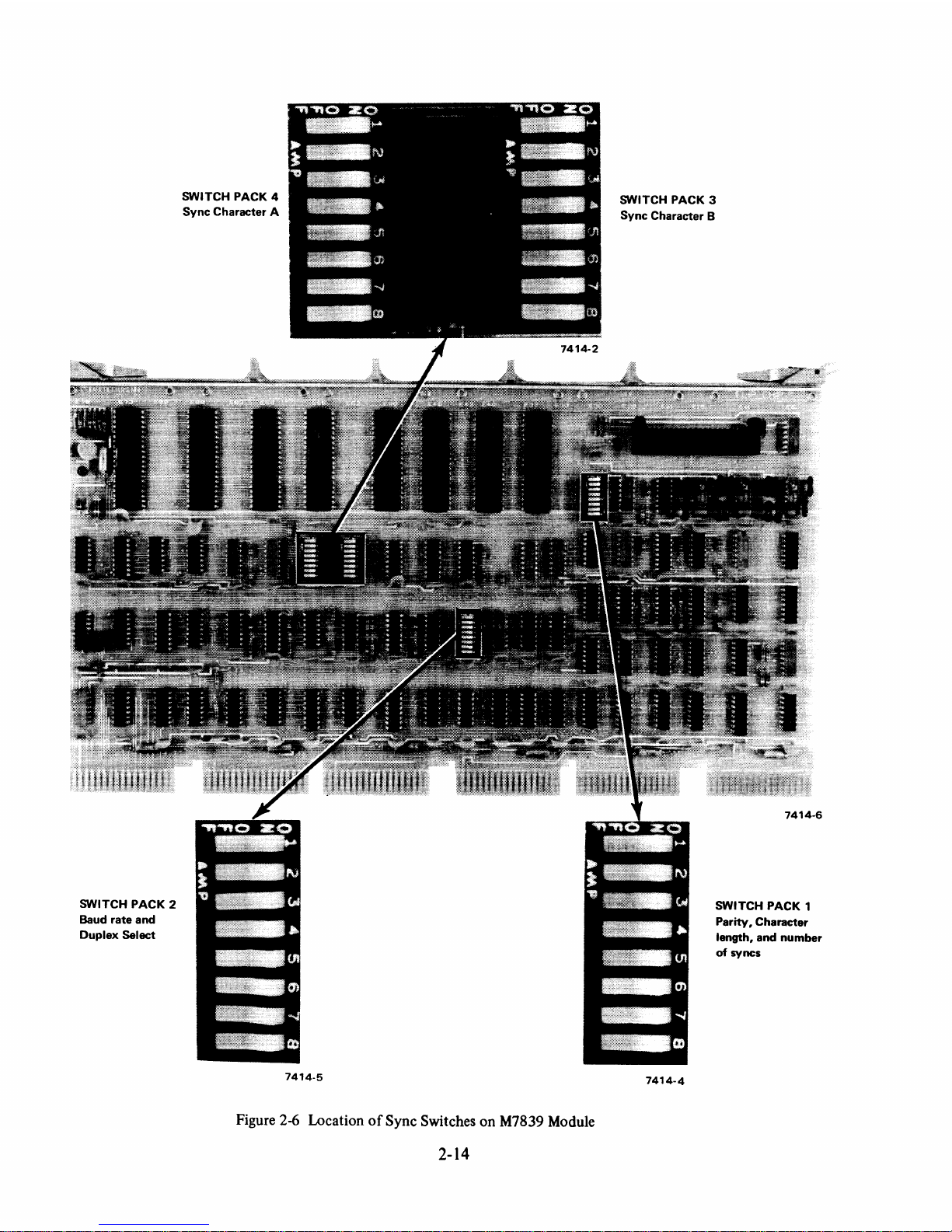
SWITCH PACK 2
Baud
rate
and
Duplex
Select
SWITCH PACK 4
Sync
Character
A
7414-5
Figure 2-6 Location
of
Sync Switches on M7839 Module
2-14
SWITCH PACK 3
Sync
Character
B
7414-4
7414-6
SWITCH PACK 1
Parity.
Character
length.
and
number
of
syncs
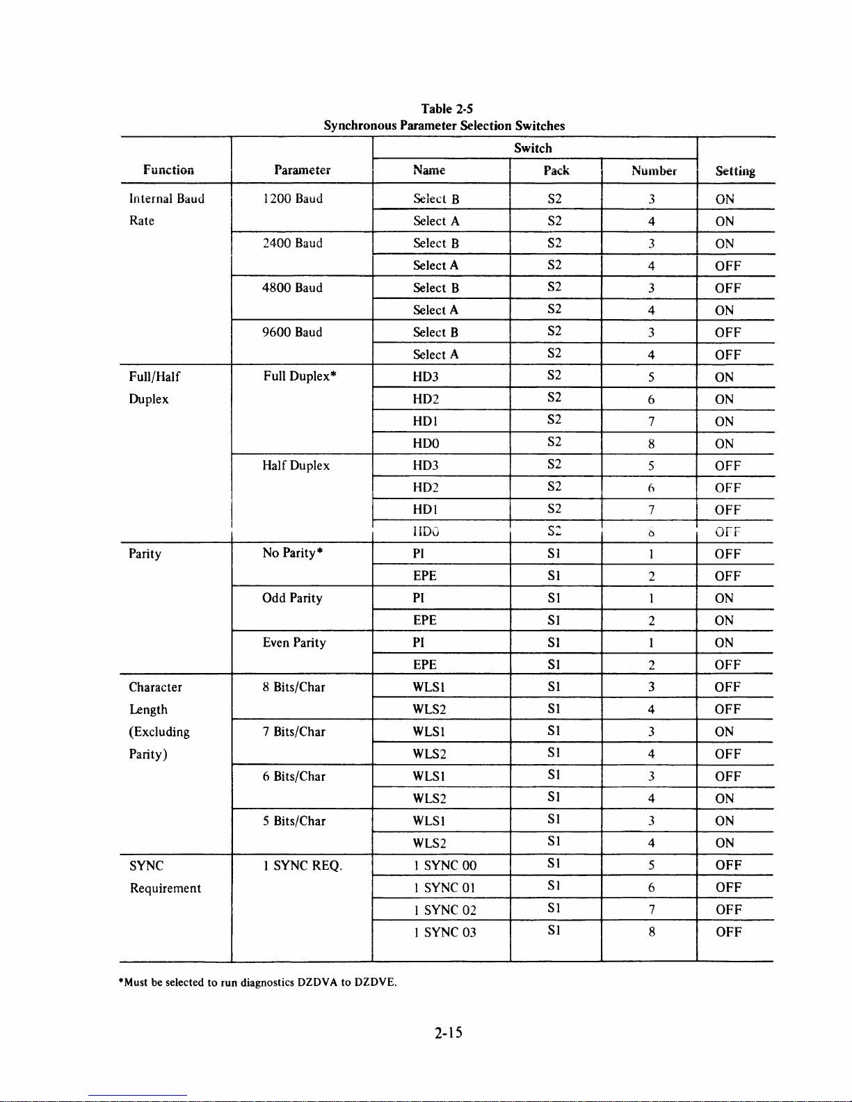
Table 2-5
Synchronous
Parameter Selection Switches
Switch
Function
Parameter Name
Pack
Number
Setting
Internal Baud
1200 Baud
Select B
S2
3
ON
Rate
Select
A
S2
4
ON
2400 Baud
~olo"t
0
~J""",",,\.U
"2
f""'\11..1
..J
V1'
S2
Select A
S2
4
OFF
4800
Baud
Select B
S2
3
OFF
Select A
S2
4
ON
9600 Baud
Select
B
S2
3
OFF
Select A
S2
4
OFF
Full/Half
Full Duplex *
HD3
S2
5
ON
Duplex HD2
S2
6
ON
HDI
S2
7
ON
HDO
S2
8
ON
Half Duplex
HD3
S2
5 OFF
HD2
S2
()
OFF
HDI
S2
7
OFF
1 U
s...,
...
0
v -r'
Parity
No Parity*
PI
SI
I
OFF
EPE
SI
2
OFF
Odd Parity
PI
SI
1
ON
EPE SI
2
ON
Even Parity
PI
SI
I
ON
EPE SI
2
OFF
Character 8 Bits/Char WLSI
SI
3
OFF
Length
WLS2
SI
4
OFF
(Excluding 7 Bits/Char
WLSI
SI
3
ON
Parity)
WLS2
SI
4
OFF
6 Bits/Char
WLSI
SI
3
OFF
WLS2
SI
4
ON
5 Bits/Char
WLSI
SI
3
ON
WLS2
SI
4
ON
SYNC
1
SYNC
REQ.
1
SYNC
00
SI
5
OFF
Requirement
1
SYNC
01
SI
6 OFF
I
SYNC
02
SI
7
OFF
I
SYNC
03
SI
8
OFF
*Must be selected
to
run diagnostics DZDV A to DZDVE.
2-15
Table 2-5 (Cont)
Synchronous Parameter Selection Switches
Switch
Function
Parameter Name
Pack Number Setting
Sync Req.
(cont)
2 SYNC REO.
1 SYNC 00
SI
5
ON
1 SYNC
01
SI
6
ON
1 SYNC 02
SI
7
ON
1 SYNC 03
Sl
8
ON
Sync Character
Desired Code
Sync A
S4
1
(As required
Codes
,j,
OFF=Logi-
8
cal
one)
Desired
Code
Sync B
S3
1
(As required
,j,
OFF=Logi-
8
cal one)
Line
synchronization
can
be
selected
by
the
receipt
of
either
one
sync
character
or
two
consecutive,
identi-
cal
sync
characters. F or
each
4-line
group,
two
sync
codes
(Sync A or
Sync
8)
may
be
manually
preset
in
the
Sync
Character
Code
switches.
The
PDP-ll
pro-
gram
may
select
either
of
these
two
sync
codes
for use
on
a selected line.
2.4.4 Installation
of
Add-On
DVll
Internal
baud
rate
is
determined
by
the
ON/OFF
states
of
the
Select A
and
Select 8 switches.
This
is
applicable
only
when
the
modem
does
not
supply
clocking.
2.4.3 Resistance Checks
Measure
the
resistance
between
the
following
pins
on
the
backplane
with
the
white
plug
of
the
7010835
cable
hanging
free
(not
plugged
in),
and
with
all
mod-
ules
plugged
in:
+5
V
to
GND
must
be 0.5 n
or
greater
-15
V
to
GND
must
be 50 n
or
greater
+
15
V
to
GND
must
be
10
n
or
greater
If
the
resistance
is less
than
the
lower
limit
indicated,
check
for a short.
If
the
resistance
exceeds five
times
the
low limit, it
may
indicate
an
open
circuit.
Make
each
measurement
twice,
once
for
each
polarity
of
the
meter.
The
lowest
reading
must
not
be less
than
the
low
limit
listed.
If
the
above
resistances
are
correct,
connect
the
white
plug
in
accordance
with
D-UA-
DVII-O-O.
2-16
Proceed
as
follows
to
install
an
add-on
DVll:
1.
Install
the
wired
backplane
assembly
in
the
mounting
box.
2.
Measure
the
resistance
between
pins
of
the
power
harness
(see first
paragraph
of
Section
2.3).
3.
Plug in
the
Mate-N-Lok
connector
of
the
power
harness.
4.
Apply
power
and
measure
voltages
at
the
logic
pins
(Paragrah
2,3),
5.
Turn
power
off.
6.
Set
all
address,
parameter
switches
(Para-
graphs
2.4.1
and
2.4.2)
and
distribution
panel
jumpers
(Figure
2-7).
7.
Install
modules
(Figure
2-2).
8.
Unplug
the
power
harness.
9.
Do
resistance
checks
(Paragraph
2.4.3).
10.
Apply
power.
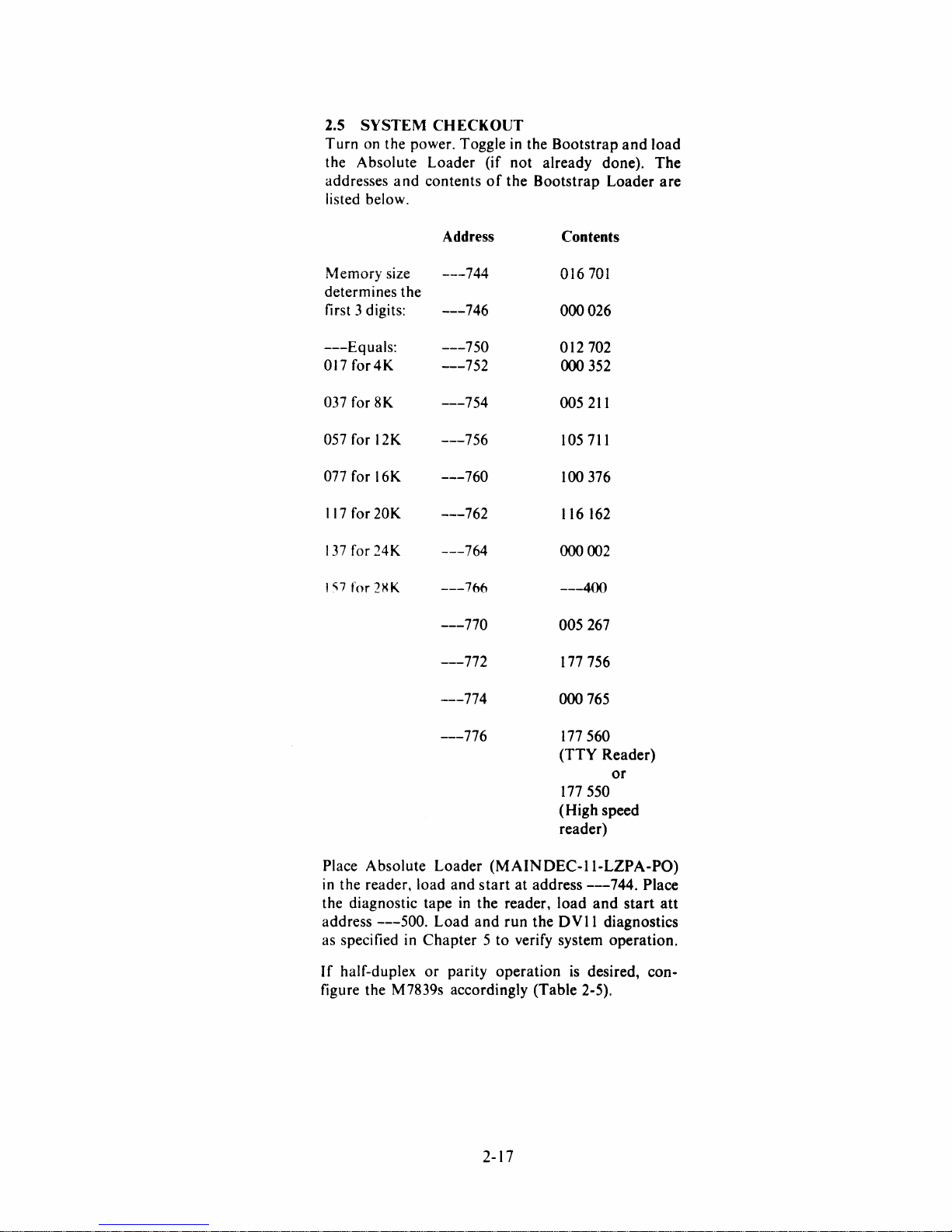
2.5
SYSTEM
CHECKOUT
Turn
on
the power. Toggle
in
the Bootstrap
and
load
the Absolute Loader (if not already done).
The
addresses
and
contents
of
the Bootstrap Loader are
listed below.
Address
Contents
l"'f~_~_
•.
~:_~
.,,,,,
1\
1 £
.,1\
1
IVI~IIIVI Y ~IL~
---I
....
VIU
IVI
determines the
first 3 digits:
---746
000 026
---Equals:
---750
012702
017for4K
---752
000
352
037
for 8K
---754
005211
057
for 12K
---756
105
711
077
for 16K
---760
100376
117
for 20K
---762
116
162
137
for 24K
---764
000
002
I "7
for
2XK
---766
---400
---770
005267
---772
177756
---774
000
765
---776
177560
(TTY Reader)
or
177550
(High speed
reader)
Place Absolute Loader
(MAINDEC-II-LZPA-PO)
in
the reader, load and
start
at address
---744.
Place
the diagnostic tape
in
the reader, load
and
start
att
address
---500.
Load and run the
DVII
diagnostics
as specified
in
Chapter 5 to verify system operation.
I f half-duplex
or
parity operation
is
desired, con-
figure the M7839s accordingly (Table 2-5).
2-17
 Loading...