


DIGISINE
ENERGYTECH
BDP-8670
DATASHEET
Oct,1Feb 2017
Version1.1
Datasheet by Yu-Hsun Lin.

Reversion History
Data
2017-10-1
Version Description Author
1.1
First Release
Yu-Hsun Lin
2

CONTENT
1. INTRODUCTION…………………………………………..... ..... ....5
1.1 D
1.2 Features…..…………………………………………………………5
1.3 Applications……..……………………………………………………5
1.4 Block Diagram………………………………………………………6
escription….……………………………………………………….5
2.GENERAL SPECIFICATION………………………………..... ...7
PHYSICAL CHARACTERISTIC..................................... .......8
3.
3.1 Pin Configurations..................................................... ……..... .....9
4.
PHSICAL INTERFACE
4.1 USB............................................................................. ..... ..... .....12
4.2 UART............................................................................. ..... ..... ..12
4.3 Programming and Debug Interface........ ... ........ ...... ... ... ... ... .13
................................................ ..... ..... 12
4.4 Analogue I/O Ports......................................................................13
4.5 LED Drivers........ ... ........ ...... ... ... ... ... ... ... ... ... ... ... ... ..... ...13
4.6 RF Port........ ... ........ ...... ... ... ... ... ... ...
4.7Audio Code Interface........ ........ .... ... ... ... ... ... . ... ... ... ... ... ....13
4.7.1 ADC........ ........ .... ... ... ... ... ... .. ... .. ... .. ... ….. ... ... ... ... ... .... 14
4.7.2 ADC Sample Rate Selection........ ...... .... ... .. ... ... ... ... ... .... 14
4.7.3 ADC Digital Gain........ .......... .... ... .. ... ..... ... ... .... ... ... .... ..14
4.7.4 DAC Sample Rate Selection........ .......... .... .. ... ... ..... ... .... ..14
4.7.4 DAC Sample Rate Selection........ .......... .... ...... ... ..... ... .... ..15
4.7.5 DAC Digital Gain........ .......... .... ... .. ... ....... ... ...... ... ... .... ..15
4.7.6 DAC Analogue Gain........ .......... .... ... .. ..... ..... ... ... .. ....... ..16
4.7.7 IEC 60958 Interface........ .......... .... ... .. ..... ...... ... ... .. ....... ..16
4.7.8 Microphone Input....... .......... .... ... .. ..... ...... ... ... …... ....... ..16
... ... ... ... ... ..... ..... ....13
4.7.8 Microphone Input....... .......... .... ... .. ..... ...... ... ... …..
4.7.9 Digital Microphone Inputs...... .......... .... ... .. ..... ... …... .......
3
. ....... ..16
..16

4.7.10 Line input...
... ..... ........ ............... .... ... .. ..... ... …... ........ ..16
4.7.11 Audio Output Stage...... ..... ....... ...... ... .... ... .. .... ... …. ... ..16
4.7.12 PCM Interface...... ..... ....... ……..... ... .... ... .. .... ... …... ... ..17
4.7.13 Digital Audio Interface(I2S). ..... ..... ….... ... ... .. .. .... ... .. .. ..17
4.8 Reset........ ... ........ ...... ... ... ... ... ... ... ... ... ... ... .... ..... ....... .....17
4.9 Battery Charger........ ... ........ ...... .... ... ... ... .... ... ... …. ... .... ...18
4.10VREG_EN... ......... ....... ... ........ ...... ... ... ...
... ... ... ... ... ... ... ...18
5.ELECTRICAL CHARACTERISTICS..... .... ........ ...... ... …...19
5.1 Absolute maximum ratings............ ............................... ...... …....19
5.2 Recommended operating conditions............ ...............................19
5.3 Battery Charger............................................. ...............................20
5.4 RF characteristics............................................. ...........................20
6.RECOMMEND PCB LAYOUT PATTERN
7.
RECOMMEND SOLDER PROFILE
8. STATEMENT
.......................................................................................23
.......................................22
...........................21
4

1.
INTRODUCTION
1.1 DESCRIPTION
BDP-8670 is a Bluetooth sub-system using CSR8670 chipset from Cambrige Silicon Radio.
The BlueCore® CSR8670™ BGA consumer audio platform for wired and wireless
applications integrates an ultra-low-power DSP and application processor with embedded flash
memory, a high-performance stereo codec, a power management subsystem, LED and LCD
drivers in a SOC IC.
BDP-8670 is slim and light so the designers can have better flexibilities for the product shapes.
FEATURES
1.2
•
Bluetooth V4.2 Compliant.
•USB and UART Host Interface.
•Integrated Switched-Mode Regulator.
•Integrated Battery Charger.
•Integrated Microphone bias.
•Integrated LED Driver.
•Built in 16-bit Stereo Codec- 95dB SNR for DAC ; Music Enhancements: SBC,MP3,and AAC+,
Fast stream code,AtpX,5-band EQ,3D stereo separation and so on.
• Multi-Configurable I2S, PCM or SPDIF Interface.
•Factory configurable to either 1.8V or 3.3V supply.
•16Mb internal flash memory (64-bit wide, 45ns); optional support for 64Mb of external SPI flash.
Supported Bluetooth Profile: HSP, HFP, A2DP, AVRCP, PBAP, MAP, SPP, iAP.
•
•Enhanced Audibility and Noise Cancellation.
•
Class2–more than 10 Meters.
•
Low Power Consumption.
•
Temperature range from -40°C to +85°C.
Weight: 0.8g.
•
1.3 APPLICATIONS
Wired or wireless Stereo headset or headphones
•
Wired or wireless sound bars
•
Smart remote controllers
•
•
Hands free car kits
•
Wearable audio with sensors
5
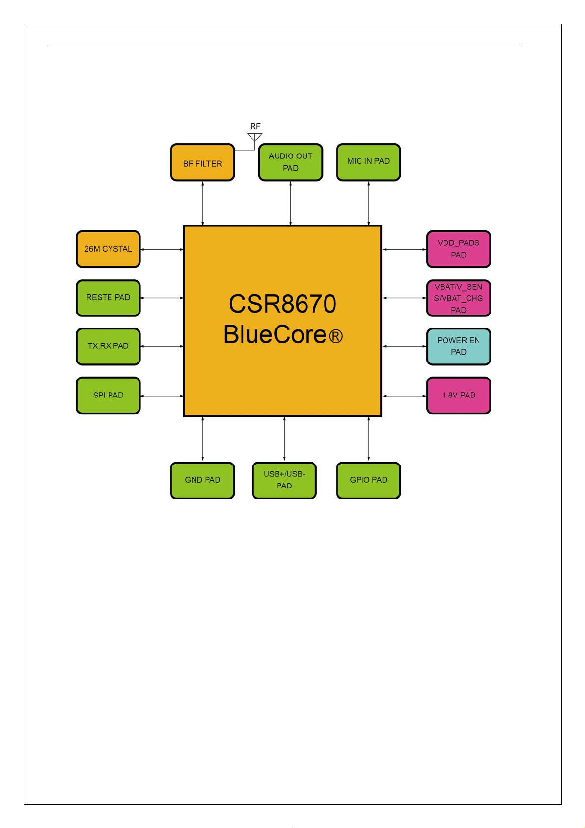
1.4 BLOCK DIAGRAM
Figure1: Block diagram of BDP-8670
6
2. GENERAL SPECIFICATIONS
Operation Freqency Band 2.400GHz-2.4835GHz unlicensed ISM band
Compliance
Max. output power 10dBm(Max)
Channels 79
Modulation Type
USB specification USB specification, version 2.0 (full- speed)
Audio interface Analogue and audio in
Dimension
Bluetooth specification,version4.2
GFSK(1
Analogue and Digital audio out
15mm x 11mm x 2.8mm.
Mbps)
7

3. PHYSICAL CHARACTERISTIC
Figure2: BDP-8670
8

3.1 PIN CONFIGURATIONS
Figure3: BDP-8670 pin description
PIN NO. NAME TYPE DESCRIPTION REMARK
1 AIO0 Bidirectional Analogue programmable input /
output line 0.
2 AIO1 Bidirectional Analogue programmable input /
output line 1.
3 GND GND Ground
4 PCM_OUT Bidirectional Synchronous Data Output,
9

with weak pull-
Alternative function PIO18
down
5 PCM_SYNC Bidirectional
with weak pull-
Synchronous Data Sync,
Alternative function PIO19
down
6 PCM_CLK Bidirectional
with weak pull-
Synchronous Data Clock,
Alternative function PIO20
down
7 PCM_IN Bidirectional
with strong pull-
Synchronous Data Input,
Alternative function PIO17
down
8 GND GND Ground
9 SPI_CLK Input with weak
Serial Peripheral Interface Clock
pull down
10 SPI_MISO Output with
weak pull down
11 SPI_CSB Input with
strong pull-up
Serial Peripheral Interface Data
Output
Chip Select For Synchronous Serial
Interface (Active
Low)
12 SPI_MOSI Input with weak
pull down
13 UART_RX Bidirectional
Serial Peripheral Interface Data
Input
UART data input. (Active High)
with strong
pull-up
14 UART_TX Bidirectional
UART Data Output (Active High)
with weak
pull-up
15 LED0 Open drain LED driver.
Alternative function PIO[29].
16 LED1 Open drain LED driver. Alternative function
PO[30].
17 LED2 Open drain LED driver. Alternative function
PO[31].
18 RESET Input with
strong pull-up
Reset if low. Input debounced so
must be low for >5ms to cause a
reset.
19 PIO4 Bidirectional
Programmable input / output line
with weak pulldown
20 PIO5 Bidirectional
Programmable input / output line
with weak pulldown
21 PIO12 Bidirectional
Programmable input / output line
with weak pulldown
22 PIO13 Bidirectional
Programmable input / output line
with weak pulldown
23 PIO6 Bidirectional
Programmable input / output line
with weak pulldown
10

24 PIO7 Bidirectional
Programmable input / output line
with weak pulldown
25 V_BAT_SE
NSE
Power supply
and control
Battery charger sense input.
Connect directly to the battery
positive pin.
26 USB_DP Bidirectional USB data plus with selectable
internal1.5kΩ pull-up resistor.
27 USB_DN Bidirectional USB data minus.
28 CHG_EXT Power supply
and control
External battery charger control.
External battery charger transistor
base control when using external
charger boost. Otherwise leave
unconnected.
29 V5_IN Power supply Charger input.
Typically connected to VBUS
(USB supply)
30 1.8V_OUT Power supply 1.8V DC/DC convertor output.
31 VDD_PADS Power supply
and control
1.7V to 3.6V positive supply input
for input/output ports:
■RST#
■UART
■PCM
■ SPI
■ PIO[15:0]
32 VDD_MEN Power supply
and control
1.7V to 3.6V positive supply input
for input/output ports:
■ Serial quad I/O flash port
33 VREG_EN Power supply
and control
Regulator enable input.
Can also be sensed as an input.
Regulator enable and multifunction
button. A high input (tolerant to
VBAT) enables the on-chip
regulators, which can then be
latched on internally and the button
used as a multifunction input.
34 VBAT Power supply
Battery positive terminal.
and control
35 GND GND Ground
36 PIO21 Bidirectional
with strong pull-
SPI flash clock.
Alternative function PIO[21].
down
37 PIO22 Bidirectional
with strong pull-
SPI RAM clock.
Alternative function PIO[22].
down
38 PIO23 Bidirectional
with strong pull-
SPI flash chip select.
Alternative function PIO[23]
up
39 PIO24 Bidirectional
with strong pull-
SPI RAM chip select.
Alternative function PIO[24].
up
11

40 PIO25 Bidirectional
with strong pull-
Serial quad I/O flash data bit 0.
Alternative function PIO[25].
down
41 PIO26 Bidirectional
with strong pull-
Serial quad I/O flash data bit 1.
Alternative function PIO[26].
down
42 PIO27 Bidirectional
with strong pull-
Serial quad I/O flash data bit 2.
Alternative function PIO[27].
down
43 PIO28 Bidirectional
with strong pull-
Serial quad I/O flash data bit 3.
Alternative function PIO[28].
down
44 GND GND Ground
45 MIC_BIAS
Analogue out Microphone bias A.
_A
46 MIC_BIAS
Analogue out Microphone bias B.
_B
47 MIC_RN
Microphone input negative, right.
48 MIC_RP Microphone input positive, right.
Analogue in
49 MIC_LN
50 MIC_LP Microphone input positive, left.
Analogue in
Microphone input negative, left.
51 GND GND Ground
52 SPK_LN Analogue Speaker output negative, left
53 SPK_LP Analogue Speaker output positive, left
54 SPK_RN Analogue Speaker output negative, right
55 SPK_RP Analogue Speaker output positive, right
56 GND GND Ground
57 RF_IN Bluetooth 50Ω transmitter output
/receiver input
58 GND GND Ground
4. PHYSICAL INTERFACE
4.1 USB
The module supports the Universal Serial Bus (USB) interface as a full speed Universal
Serial Bus for communicating with other compatible digital devices. The USB interface acts as a
USB peripheral, responding to requests from a master host controller such as a Personal
Computer(PC).The module contains internal USB termination resistors and requires no external
resistor matching.
The module supports the Universal Serial Bus Specification, Revision v2.0 (USB v2.0
Specification), supports USB standard charger detection and fully supports the USB Battery
Charging Specification .
12

4.2 UART
The module has one optional standard UART serial int
mechanism for communicating with other serial devices using the RS232 protocol, including
for test and debug. The UART interface is multiplexed with PIOs and other functions, and
hardware flow control is optional.
erface that provides a simple
4.3 Programming and Debug Interface
A debug SPI interface is supplied for programming, configuring (PS Keys) and
debugging Access to this interface is required in production.
Tonly provides development and production tools to communicate over the SPI from a
PC, although a level translator circuit is often required. All are available from Tonly.
4.4 Analogue I/O Ports
he general-purpose analogue interface pins, AIO_0,AIO_1, are supplied by the module.
T
Typically, this connects to a thermistor for battery pack temperature measurements during charge
control.
4.5 LED Drivers
An 3-pad synchronised PWM LED driver is supplied for driving RGB LEDs for producing a
wide range of colours. All LEDs are controlled by firmware.
The terminals are open-drain outputs, so the LED must be connected from a positive supply
rail to the pad in series with a current-limiting resistor.
4.6 RF Port
An on-chip balun combines the balanced outputs of the PA on transmit and produces the
alanced input signals for the LNA required on receive. No matching components are needed as
b
the receive mode impedance is 50Ω and the transmitter has been optimised to deliver power into a
50Ω load.
4.7 Audio code Interface
The main features of the interface are:
Stereo and mono analogue input for voice band and audio band .
Stereo and mono analogue output for voice band and audio band .
Support for stereo digital a udio bus standards such as I2S.
Support for IEC -60958 standard stereo digital audio bus standards, e.g. SPDIF and
AES3(also known as AES/EBU).
Support for PCM interfaces including PCM master c oded that require an external
system clock.
13

Figure4 (Audio Codec Input and Output Stages)
4.7.1 ADC
Figure 4 shows the CSR8670 consists of 2 high-quality ADCs:
Each ADC has a second -order Sigma-Delta converter
Each ADC is a separate channel with identical functionality
There are 2 gain stages for each channel,1 of which is an analogue gain stage and the
other is a digital gain stages
4.7.2 ADC Sample Rate Selection
Each ADC supports the following pre-defined sample rates, although other rates are
programable,e.g.40kHz:
8kHz
11.025 kHz
16kHz
22. 050kHz
24kHz
32 kHz
44.1kHz
48 kHz
4.7.3 ADC Digital Gain
A digital gain stage inside the ADC varies from -24dB to 21.5dB,see as below, there is also a
fine gain interface with 9-bit gain setting allowing gain changes in 1/32 steps.
The Firmware controls the audio input gain.
14

4.7.4 DAC Sample Rate Selection
8kHz
11.025kHz
16kHz
22.050kHz
32kHz
40kHz
44.1kHz
48kHz
96kHz
4.7.5 DAC Digital Gain
A digital gain stage inside the DAC varies from -24dB to 21.5dB, see as below, there is also a
Fine gain interface with 9-bit gain setting enabling gain changes in 1/32 steps.
The overall gain control of the ADC is controlled by the firmware. Its setting is a combined.
function of the digital and analogue amplifier settings
15

4.7.6 DAC Analogue Gain
As below shows that the DAC analogue gain stage consists of 8 gain selection values that
represent seven 3dB steps.
The firmware controls the overall gain control of the DAC. Its setting is a combined function of
the digital and analogue amplifier settings.
4.7.7 IEC 60958 Interface
The IEC 60958 interface is a digital audio interface that uses bi-phase coding to minimise the
DC content of the transmitted signal and enables the receiver to decode the clock information from
the transmitted signal. The IEC 60958 specification is based on the 2 industry standards:
AES3( also known as AES/EBU)
Sony and Philips interface specification SPDIF
The interface is compatible with IEC 60958-1, IEC 60958-3 and IEC 60958-4
The SPDIF interface signals are SPDIF-IN and SPDIF-OUT and are shared on the PCM
interface pin.
4.7.8 Microphone Input
The CSR8670 contains 2 independent low-noise microphone bias generators. The microphone
bias generators are recommended for biasing electret condensor micro phones. A biasing circuit
for microphones with a sensitivity between about -40dB to -60dB(0dB=1V/Pa).
4.7.9 Digital Microphone Inputs
The CSR8670 interfaces to 6 digital MEMS microphones. Figure 4 shows that 4 of
the inputs have dedicated codec channels and 2 are multiplexed with the high quality
ADC channels.
4.7.10 Line input
If the pre-amplifier audio input gain is set at a low gain level it acts as an audio
line level amplifier. In this line input mode the input impendance varies from 6kohm to
30kohm,depending on the volume setting.
4.7.11 Audio Output Stage
The output digital circuitry converts the signal from 16-bit per sample, linear PCM of variable
sampling frequency to a 2Mbits/sec multi-bit stream, which is fed into the analogue output
circuitry.
The output circuit comprises a digital to analogue converter with gain setting and output
Amplifier. Its class-AB output-stage is capable of driving a signal on both channels of up to 2V
pk-pk differential into a load of 16Ω. The output is available as a differential signal between
SPK_RP and SPK_RN for the right channel ; and between SPK_LP and SPK_LN for the left
16

channel. The output is capable of driving a speaker directly if its impedance is at least 8Ω if only
one channel is connected or an external regulator is used.
The gain of the output stage is controlled by a 3-bit programmable resistive divider, which sets
the gain in steps of approximately 3dB.
The multi-bit stream from the digital circuitry is low pass filtered by a second order biquad
filter with a pole at 20kHz. The signal is then amplified in the fully differential output
stage, which has a gain bandwidth of typically 1MHz.
4.7.12 PCM Interface
The audio PCM interface on the TBM_C870 supports:
On -chip routing to Kalimba DSP.
Continuous transmission and reception of PCM encoded audio data over Bluetooth.
Processor overhead reduction through hardware support for continual transmmision
And reception of PCM data
A bidirectional digital audio interface that routes directly into the baseband layer of
the firmware .It does not pass through the HCI protocol layer.
Hardware on the TBM_C870 for sending data to and from a SCO connection.
Up to 3 SCO connections on the PCM interface at any one time.
PCM interface master, generating PCM_SYNC and PCM_CLK.
PCM interface slave, accepting externally generated PCM_SYNC and PCM_CLK.
Various clock formats including:
Long Frame Sync
Short Frame Sync
GCI timing environments
13 -bit or 16-bit linear,8-bit u-law or A-law companded sample formats.
Receives and transmits on any selection of 3 the first 4 slots following PCM_SYNC. The
PCM configuration options are enabled by setting the PS Key .PSKEY_PCM_CONFIG32.
4.7.13 Digital Audio Interface(I2S)
The digital audio interface supports the industry standard formats for I2S,left-justified or right
justified.
The interface shares the same pins as the PCM interface, which means each audio bus is mutually
exclusive in its usage. Table as below lists these alternative functions
4.8 Reset
The BT_Reset pin is an active low reset and is internally filtered using the internal low frequency
clock oscillator. Tonly recommends applying BT_Reset for a period >5ms.
17

4.9 Battery Charger
The internal charger circuit can provide up to 200mA of charge current, for current
s higher than
this , you should use external charger mode.
The external mode is for charging higher capacity batteries using an external pass device. The
current is controlled by sinking a varying current into the CHG_EXT pin, and the current is
determined by measuring the voltage drop across a resistor, Rsense, connected in series with the
external pass device. The voltage drop is determined by looking at the difference between the
VBAT_SENSE and VBAT pins. The voltage drop across Rsense is typically 200mV. The value of
the external series resistor determines the charger current. This current can be trimmed with a PS
Key.
4.10 VREG_EN
The module boots-up when this VR
enableing the regulators in the module. The firmware then latches the regulators on. The voltage
regulator enable pin can then be released. The status of the VREG_EN pin is available to firmware
through an internal connection. VREG_EN pin should be asserted after the VBAT supply when
VREGENABLE is not used as a power-on button.
EG_EN pin is pulling high typically for 10 to 15ms,
18

Rating
Min Max Unit
Storage temper
ature -40
105 °C
Supply Voltage
VCHG
-0.40
5.75
V
VBAT
-0.40
4.40
V
VREG
-0.40
4.40
V
VDD_PADS
-0.40
3.60
V
Rating
Min Max Unit
Operating temperature
-
40
85 °C
Supply Voltage
VCHG
4.75
5.75
V
VBAT
2.5 4.25 V
VREG
0
4.25
V
5.ELECTRIAL CHARACTERSTICS
5.1 Absolute maximum ratings
The module should not continuously run under these conditions. Exposure to absolute maximum rating
conditions for extended periods of time may affect reliability and cause permanent damage to the device.
Table1: Absolute maximum ratings
5.2 Recommended operating conditions
VDD_PADS
Table2: Recommended operating conditions
1.8
3.60
V
19

5.3 Battery Charger
Trickle Charge Mode M
in Type Max Unit
Charge current I trickle, as percentage of fast charge current 8 10 12 %
V fast rising threshold - 2.9 - V
V fast falling threshold - 2.8 - V
Fast Charge Mode
Charge current during constant current mode, Ifast
194 200 206 mA
Maximum charge setting(VCHG-VBAT > 0.55V)
Fast charge current, Ifast (External Charge Mode(a)) 200 500 mA
V float threshold, calibrated 4.16 4.20 4.24 V
Charge termination current Iterm, as percentage of fast 7 10 20 %
Standby Mode
Voltage hysteresis on VBAT, Vhyst 100 150 mV
(a) In the external mode, the battery charger meets all the previous charger electrical characteristics and the additional or
superseded electrical characteristics are listed in this table.
Table3: Battery charger
5.4 RF characteristics
Transmi
tter
Output
Power
Chann
Average Bluetooth
el
2402 4.00
dBm
2441 4.80 dBm
2480 4.97 dBm
Receiver Chann
Spec.
-6 dBm
~+10 dBm
Sensitivity at
0.1% BER
Table4:RF characteristics
Average Bluetooth
el
Spec.
2402 -81 dBm <=-70dBm
2441 -81 dBm
2480 -81 dBm
20

6. RECOMMEND PCB LAYOUT PATTERN
Figture4 Recommended PCB land pattern for BDP-8670
21

7.
RECOMMEND SOLDER PROFILE
The soldering profile depends on various parameters necessitating a set up for each
application. The data here is given only for guidance on solder re-flow. There are four zones:
1. Preheat Zone - This zone raises the temperature at a controlled rate, typically 1-2.5°C/s.
2. Equilibrium Zone - This zone brings the board to a uniform temperature and also
activates the flux. The duration in this zone (typically 2-3 minutes) will need to be adjusted to
optimize the out gassing of the flux.
3. Reflow Zone - The peak temperature should be high enough to achieve good wetting but
not so high as to cause component discoloration or damage. Excessive soldering time can lead
to intermetallic growth which can result in a brittle joint.
4. Cooling Zone - The cooling rate should be fast, to keep the solder grains small which
will give a longer lasting joint. Typical rates will be 2-5°C/s.
Figture5 Recommended solder profile
Key features of the profile:
■ Initial ramp = 1-2.5°C/sec to 175°C ±25°C equilibrium
■ Equilibrium time = 60 to 180 seconds
■ Ramp to maximum temperature (245°C) = 3°C/sec max.
■ Time above liquidus temperature (217°C): 45-90 seconds
■ Device absolute maximum reflow temperature: 260°C
22

8.
S
TATEMENT
This device complies with part 15 of the FCC Rules. Operation is subject to the following
two conditions: (1) This device may not cause harmful interference, and (2) this device must
accept any interference received, including interference that may cause undesired operation.
This equipment has been tested and found to comply with the limits for a Class B digital
device, pursuant to part 15 of the FCC Rules. These limits are designed to provide reasonable
protection against harmful interference in a residential installation. This equipment generates,
uses and can radiate radio frequency energy and, if not installed and used in accordance with the
instructions, may cause harmful interference to radio communications. However, there is no
guarantee that interference will not occur in a particular installation. If this equipment does
cause harmful interference to radio or television reception, which can be determined by turning
the equipment off and on, the user is encouraged to try to correct the interference by one or
more of the following measures:
—Reorient or relocate the receiving antenna.
—Increase the separation between the equipment and receiver.
—Connect the equipment into an outlet on a circuit different from that to which the receiver is
connected.
—Consult the dealer or an experienced radio/TV technician for help.
Any changes or modifications not expressly approved by the party responsible for
compliance could void the authority to operate
equipment.
This device and its antenna must not be co-
located or operating in conjunction with any other antenna or transmitter.
End-users and installers must be provided with antenna installation instructions and
transmitter operating conditions for satisfying RF
exposure compliance.
This equipment complies with FCC radiation exposure limits set forth for an uncontrolled
environment. This equipment should be installed and operated with minimum distance 20cm
between the radiator & your body.
Module
This module is intended for OEM integrator. The OEM integrator is still responsible for
the FCC compliance requirement of the end product, which integrates this module. 20cm
minimum distance has to be able to be maintained between the antenna and the users for the
host this module is integrated into. Under such configuration, the FCC radiation exposure limits
set forth for an population/uncontrolled environment can be satisfied.
Any changes or modifications not expressly approved by the manufacturer could void the user's
authority to operate this equipment.
USERS MANUAL OF THE END PRODUCT:
In the users manual of the end product, the end user has to be informed to keep at least
20cm separation with the antenna while this end product is installed and operated. The end user
has to be informed that the FCC radio-frequency exposure guidelines for an uncontrolled
environment can be satisfied. The end user has to also be informed that any changes or
modifications not expressly approved by the manufacturer could void the user's authority to
operate this equipment.
23

If the size of the end product is smaller than 8x10cm, then additional FCC part 15.19
statement is required to be available in the user’s manual: This device complies with Part 15 of
FCC rules. Operation is subject to the following two conditions: (1) this device may not cause
harmful interference and (2) this device must accept any interference received, including
interference that may cause undesired operation.
LABEL OF THE END PRODUCT:
The final end product must be labeled in a visible area with the following " Contains TX
FCC ID: VLV867029165569". If the size of the end product is larger than 8x10cm, then the
following FCC part 15.19 statement has to also be available on the label: This device complies
with Part 15 of FCC rules. Operation is subject to the following two conditions: (1) this device
may not cause harmful interference and (2) this device must accept any interference received,
including interference that may cause undesired operation.
24
 Loading...