

Page 1

EDK Base System Builder
(BSB) support for XUPV2P
Board
Xilinx University Program
May 2005
Page 2

What is BSB?
• The Base System Builder (BSB) wizard is a software tool that help users quickly
build a working system targeted at a specific development board.
• Based on the user’s board selection, BSB will offer the user a number of options
for creating a basic system on that board. These options include processor type,
debug interface, cache configuration, memory type and size, and peripheral
selection. For each option, functional default values will be preselected in the
GUI.
• Upon exit of BSB, a hardware specification (MHS) file and software specification
(MSS) file will be created and loaded into the user’s XPS project. The user may
then optionally further enhance the design in the Xilinx Platform Studio (XPS)
GUI.
• The Base System Builder will also optionally generate a software project called
“TestApp” which contains a sample application and linker script and can be
compiled and run on the hardware on the target development board. Note that
XPS supports multiple software projects for every hardware system, each of
which may contain its own set of source files and linker script.
• Chapter 3 of the EDK System Tools Manual is good reference:
– http://www.xilinx.com/ise/embedded/est_rm.pdf
May 2005XUPV2P BSB support 2
Page 3

Objective
• Use a BSB design (or derivative) as the basis for:
– Standalone processor based designs
– Board Support Packages for PP405 Linux and
Microblaze uCLinux
• Since it is a general tool, BSB designs are not
optimum for every configuration but provide a
starting point for further development since it
provides reasonable defaults for all parameters
not changed by the user
May 2005XUPV2P BSB support 3
Page 4
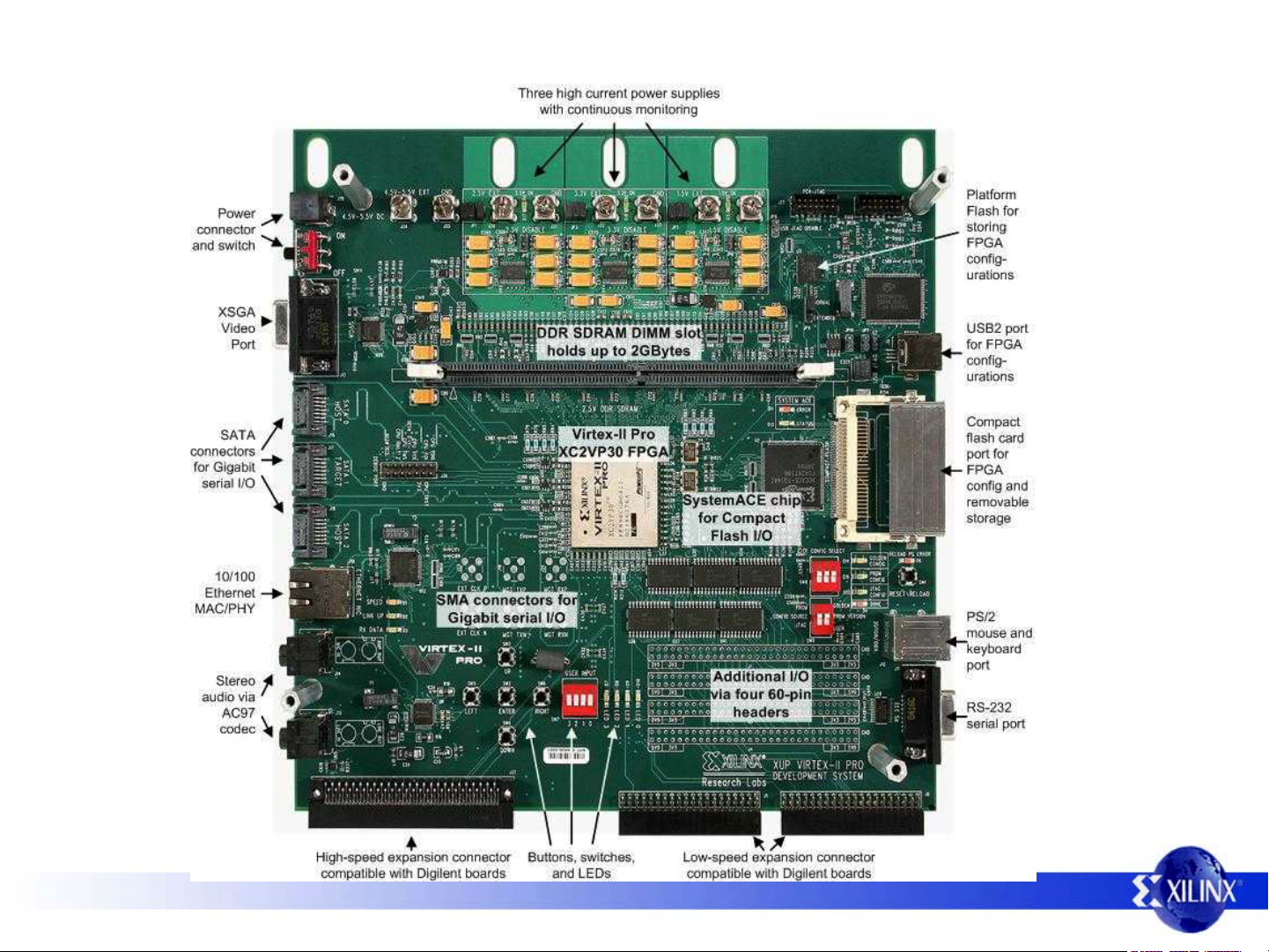
XUPV2P Development System
May 2005XUPV2P BSB support 4
Page 5
Mini-Howto
• Use EDK 7.1 SP1 (H.11.3) and ISE 7.1 SP2 (H.40)
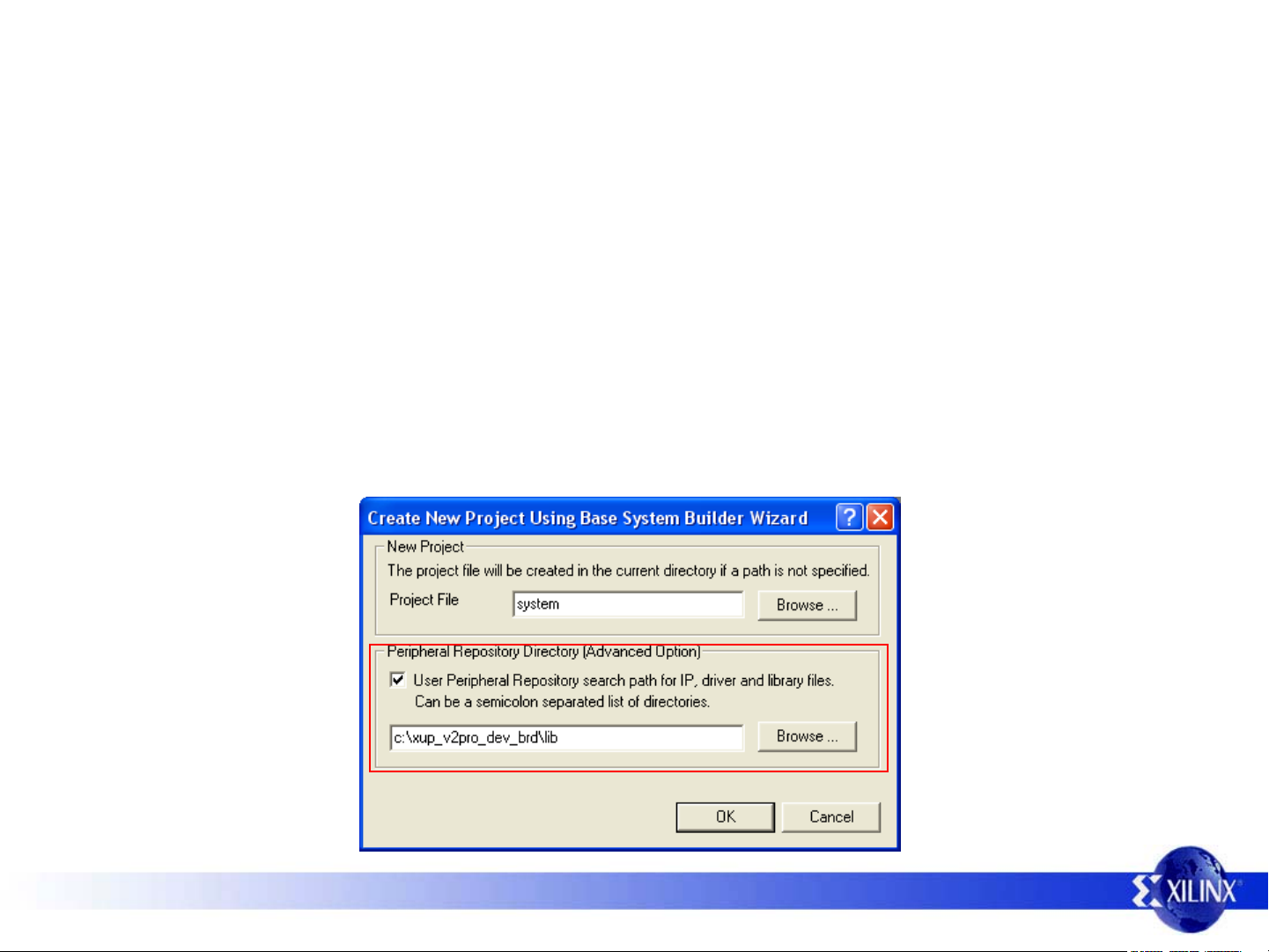
• Launch EDK Platform Studio (XPS) and select BSB flow
– Point the User Peripheral Repository Directory to the EDK
XUP-V2P support files
May 2005XUPV2P BSB support 5
Page 6
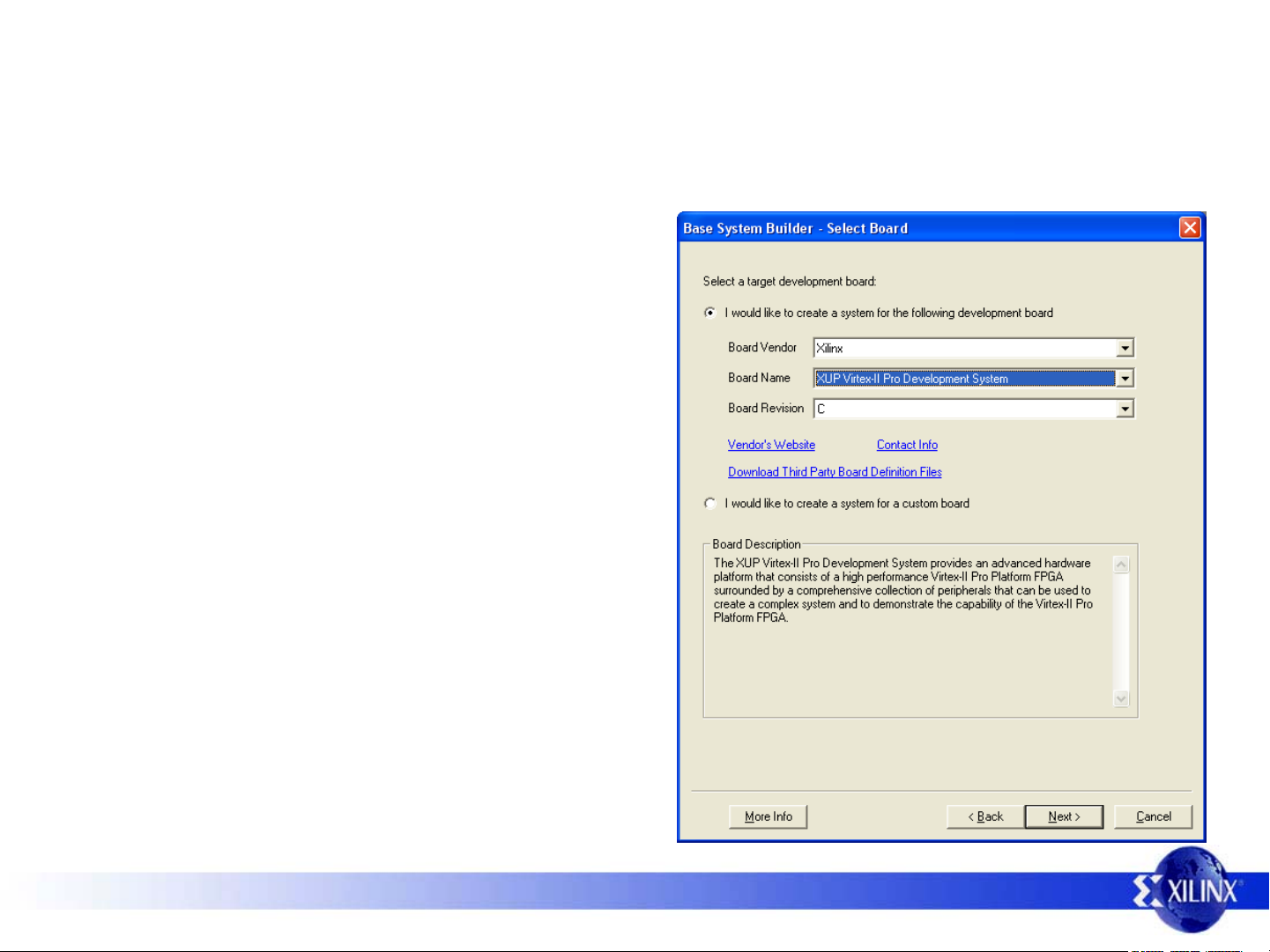
BSB Board Selection
• Select “I would like to
create a new design”
versus using a previous
BSB session as a
starting point
• The “XUP Virtex-II Pro
Development System”
should be listed under
the Xilinx board vendor
May 2005XUPV2P BSB support 6
Page 7
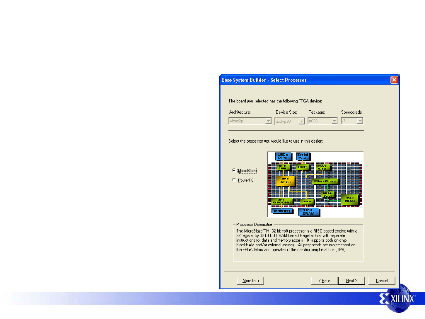
BSB Processor Selection
• BSB supports both the
PowerPC405 and
Microblaze processors,
select the Microblaze
processor for now
May 2005XUPV2P BSB support 7
Page 8

BSB Processor Options
• Accept the default
Microblaze Processor
Options
May 2005XUPV2P BSB support 8
Page 9

BSB Peripheral Selection
• The user can now include various peripherals
provided on the board and select among
parameters for each peripheral
– Select to include RS232_UART_1, LEDs_4Bit,
DIPSWs_4Bit, and PushButtons_5Bit
• BSB will optionally create example software
applications (TestApps)
– Accept default options
May 2005XUPV2P BSB support 9
Page 10

BSB System Overview
• Finally BSB lists the
system
configuration
summary for the
generated design
May 2005XUPV2P BSB support 10
Page 11

EDK Xilinx Platform Studio (XPS)
• After BSB finishes, XPS provides several options
for the next path ! Select Download the design
– Any of these operations can be performed from the
main XPS window
– However, before the design can be downloaded, it
must first be implemented
May 2005XUPV2P BSB support 11
Page 12

Design Implementation
• A bunch of things happen under the hood!!
– An HDL representation of the design will be created in the hdl directory
– Each submodule is synthesized into netlists stored in subdirectories under
implementation
– Ngdbuild combines the netlists and performs DRCs
– The netlist is placed and routed (par) and a bitfile is generated
– The software device drivers are compiled into libraries
– The user application is compiled and linked against the libraries to created
an executable elf file
– Finally, the BRAMs in the bit file which comprise the program memory are
configured with the contents of the elf file
– Implementation/download.bit is the file to program the FPGA!
May 2005XUPV2P BSB support 12
Page 13

Serial Output
• Connect a RS232 serial cable from the XUP-V2P board
serial port to the PC
• Open a terminal (i.e., HyperTerminal) for 9600baud,
8data bits, No Parity, 1 Stop bit and No flow control
May 2005XUPV2P BSB support 13
Page 14

You’ve Done It!
You have just implemented a
System-on-Chip Design
using a Xilinx FPGA!
May 2005XUPV2P BSB support 14
Page 15

TestApplication
• BSB also generates a simple test application
– Each IO EDK peripheral is wiggled by software
– LEDs are flashed and the Switches/Pushbuttons are
read
• First, enable the TestApp_Peripheral
• Then, uncomment the xil_printfs so that the state
of the switches/pushbuttons are displayed
May 2005XUPV2P BSB support 15
Page 16
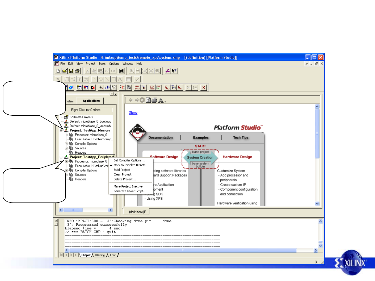
Interfacing with Peripherals
1) Disable “Mark
to Initialize
BRAMs”
1) Enable “Mark
to Initialize
BRAMs”
May 2005XUPV2P BSB support 16
Page 17
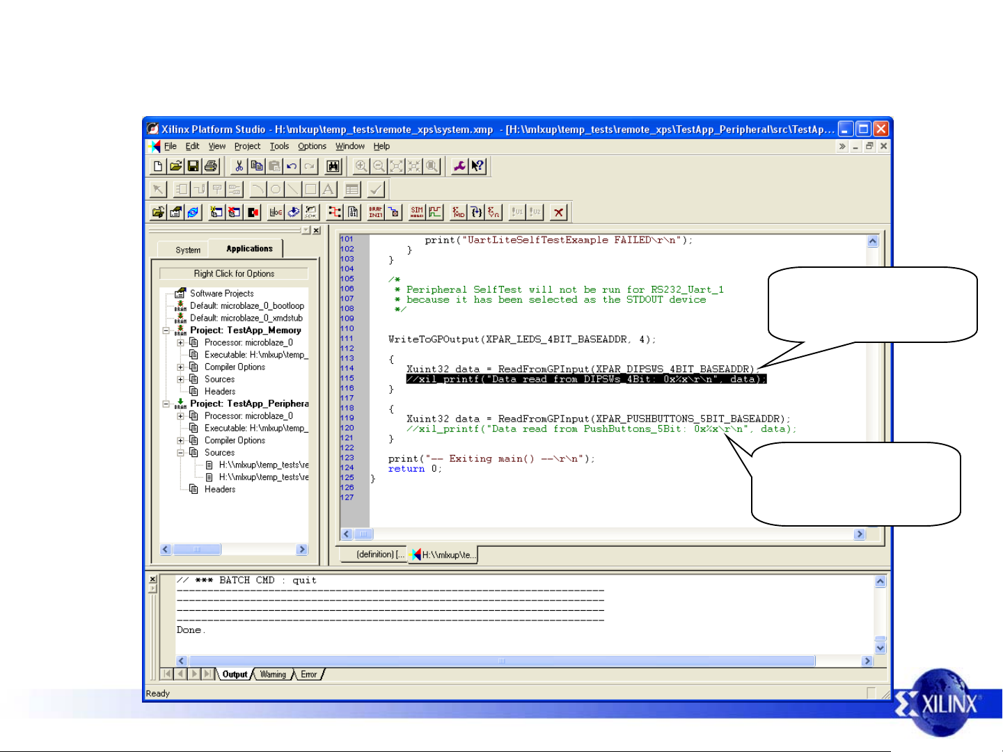
TestApplication Modification
Uncomment to
print values
Uncomment to
print values
May 2005XUPV2P BSB support 17
Page 18

Downloading the TestApp
• Select Tools!Download and the software is recompiled,
programmed into the FPGA bitstream, and then
downloaded to the board
The FPGA was configured
twice. The second time the
two left DipSwitches were
moved to the up position
resulting in different values
being read.
May 2005XUPV2P BSB support 18
Page 19
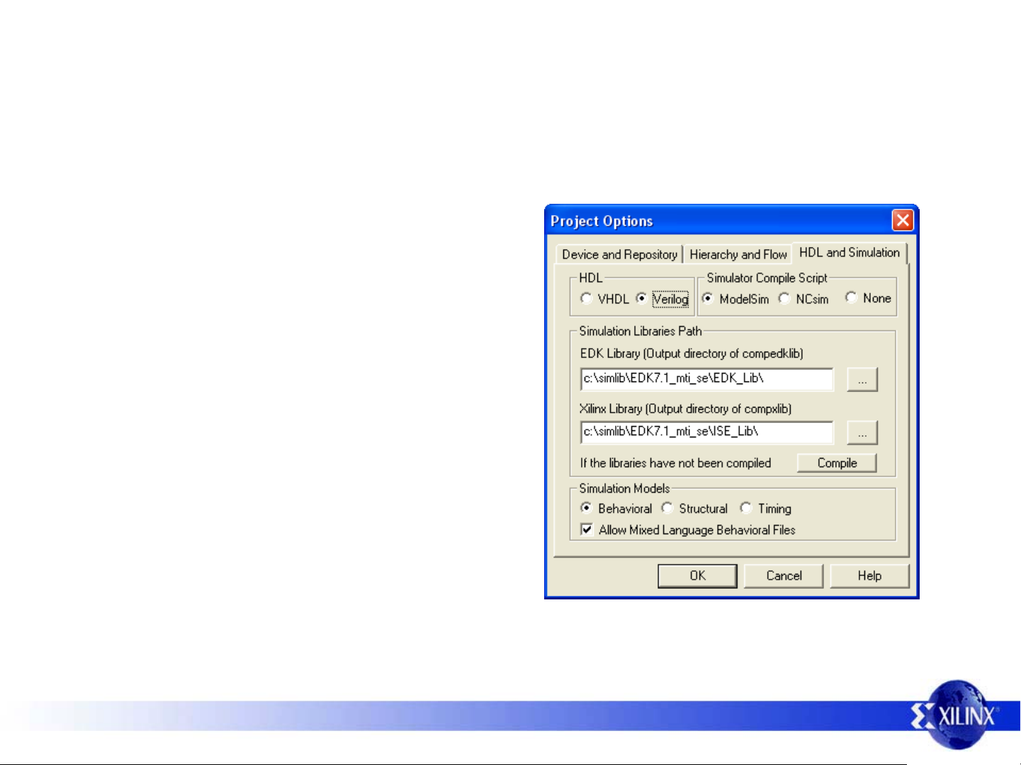
Simulation Setup
• Select Options!Project
Options and either point to
already compiled libraries or
compile them new
– Note: For PowerPC405
simulations, also need to set
up SmartModel SWIFT
support. See “Simulation in
EDK” in the “Platform Studio
User Guide”
May 2005XUPV2P BSB support 19
Page 20

Simulation Script
• Select Tools!Start HDL Simulator
– Enter the following commands (or as a do
script) at the modelsim prompt
– Note: Do not have external peripherals
modeled
May 2005XUPV2P BSB support 20
Page 21

Modelsim Simulation Commands
# Make sure to set EDK to compile for verilog
do system.do
vsim system system_conf glbl
add wave -radix hexadecimal /*
# Enable the viewing of the Microblaze registers ...
set mb_register_path "/system/microblaze_0/microblaze_0/data_flow_i"
# ... add them to the modelsim view window
quietly WaveActivateNextPane
add wave -noupdate -divider {CPU Registers}
add wave -radix hexadecimal -label PC $mb_register_path/pc_ex
add wave -radix hexadecimal -label MSR $mb_register_path/msr
force sys_rst_pin 0, 1 1us
force sys_clk_pin 0, 1 5ns -r 10ns
run 100us
May 2005XUPV2P BSB support 21
Page 22
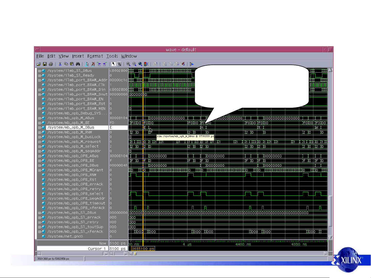
Waveform Output
“Ente” being sent to the
JTAG UART (part of the
actual data transmission)
May 2005XUPV2P BSB support 22
Page 23

Design Size and
Implementation Time
• Design Size: Currently only 3% of 2VP30 FPGA
for entire Microblaze design
– There is a lot of room for more peripherals!
• Implementation Time from start to finish:
Half Hour!
May 2005XUPV2P BSB support 23
 Loading...