

Page 1
DDiiggiilleenntt XXCCRRPP™™
RReeffeerreennccee MMaannuuaal
Revision: 04/12/05
l
www.digilentinc.com
215 E Main Suite D | Pullman, WA 99163
(509) 334 6306 Voice and Fax
Overview
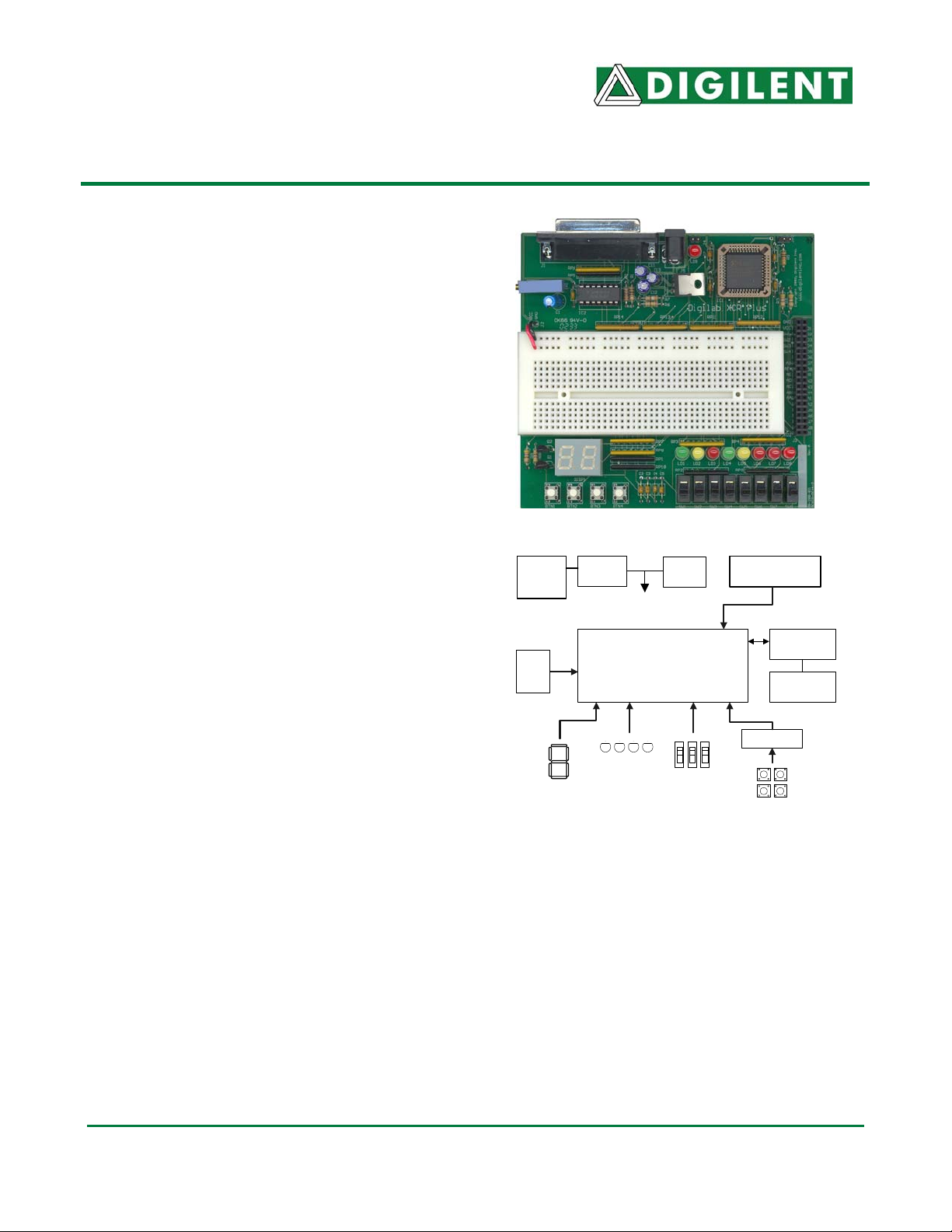
The Digilab XCRP circuit board, built around
the Xilinx CoolRunner XC3064 CPLD, provides
a very low cost platform that can be used to
implement a wide variety of digital circuits,
from complex combinational devices to
sequential machines and controllers. The
XCRP board provides an ideal platform for new
engineers requiring experience with basic
digital design techniques, as well as those
needing exposure to Xilinx CAD tools and
CPLD devices. XCRP board features include:
• A socketed Xilinx XCR3064 CPLD
• Non-volatility – designs remain in the CPLD
after power is removed
• On board voltage regulator for use with a
wall-plug transformer, or the board can run
Power
jack
5-9VDC
3.3VDC
regulator
Vcc
2 AA
cells
Adjustable clock
(0. 5Hz to 4KHz)
more than 60hrs on 2 AA cells (typical)
• Expandability –an integral solderless
breadboard allows expansion circuits to be
constructed right on the XCRP board
JTAG
Port
XCR3064XL CoolRunner
CPLD PC-44 (s ock et ed)
• Four debounced buttons
• Eight slide switches
• Eight LEDs in three colors (red, green, and
yellow)
• 40-pin expansion connector
• JTAG programming using a standard
parallel cable (included)
• Two high-bright seven segment displays
8 LEDs
2 7-seg.
displays
8 switches
XCRP Circuit Diagram
Debounce
4 buttons
• An user-adjustable oscillator circuit
(approximately 0.5Hz to 4KHz).
The XCRP board makes an excellent platform
for instructional-lab based work: it is fully
compatible with all versions of the Xilinx CAD
tools, including the free WebPack tools
available at the Xilinx website; the included
CPLD uses non-volatile configuration memory,
so designs can be completed outside the lab;
and the board ships with a programming cable
and a power source, so designs can be
implemented immediately without the need for
any additional hardware.
Functional description
The XCRP board has been designed to offer a
low-cost system for designers who need a
flexible platform to gain exposure to the basics
of digital design or to CPLD devices. The
XCRP board provides sufficient I/O devices so
that many interesting circuits can be
implemented without the need for any other
Doc: 502-021 page 1 of 1
Copyright Digilent, Inc. All rights reserved. Other product and company names mentioned may be trademarks of their respective owners.
Expansion
Connector
Solderless
breadboard
®
Page 2
XCRP Reference Manual Digilent, Inc.
devices. All CPLD signals are routed to an
expansion connector so that designs can
easily be extended using the on-board
solderless breadboard, or by attaching
accessory boards. The board can run on two
AA cells, so designs are portable. It includes a
XCR3064 CoolRunner CPLD, a JTAG
configuration circuit that uses a standard
parallel cable, a user-settable oscillator circuit,
and several useful I/O devices.
Table 1 shows all signals routed on the XCRP
board. These signals and their circuits are
described in the following sections.
Power Supplies
VBAT Battery voltage
VEXT External voltage applied to J4
VCC System voltage (VBAT or VEXT)
GND System ground routed to all devices
Programming parallel port
TDI JTAG data input signal
TCK JTAG clock signal
TMS JTAG test mode select signal
TDO JTAG data out signal
On board devices
MCLK Master clock from user-settable oscillator
BTN1-4 Debounced button inputs
SW1-8 Slide switch inputs
LED1-8 Individual LED drive signals
CAT1, 2 Common cathode signals for 7Seg displays
AA-AG Anode signals for seven segment displays
Expansion Connector
NA All signals routed to connector (except MCLK)
box. Attach the programming cable, and start
the iMPACT programmer. The board will be
auto-detected by the Xilinx software, and all
normal JTAG operations will be available.
Operations are available in a pull-down menu
made visible by right clicking on the device
graphic in the iMPACT programmer window.
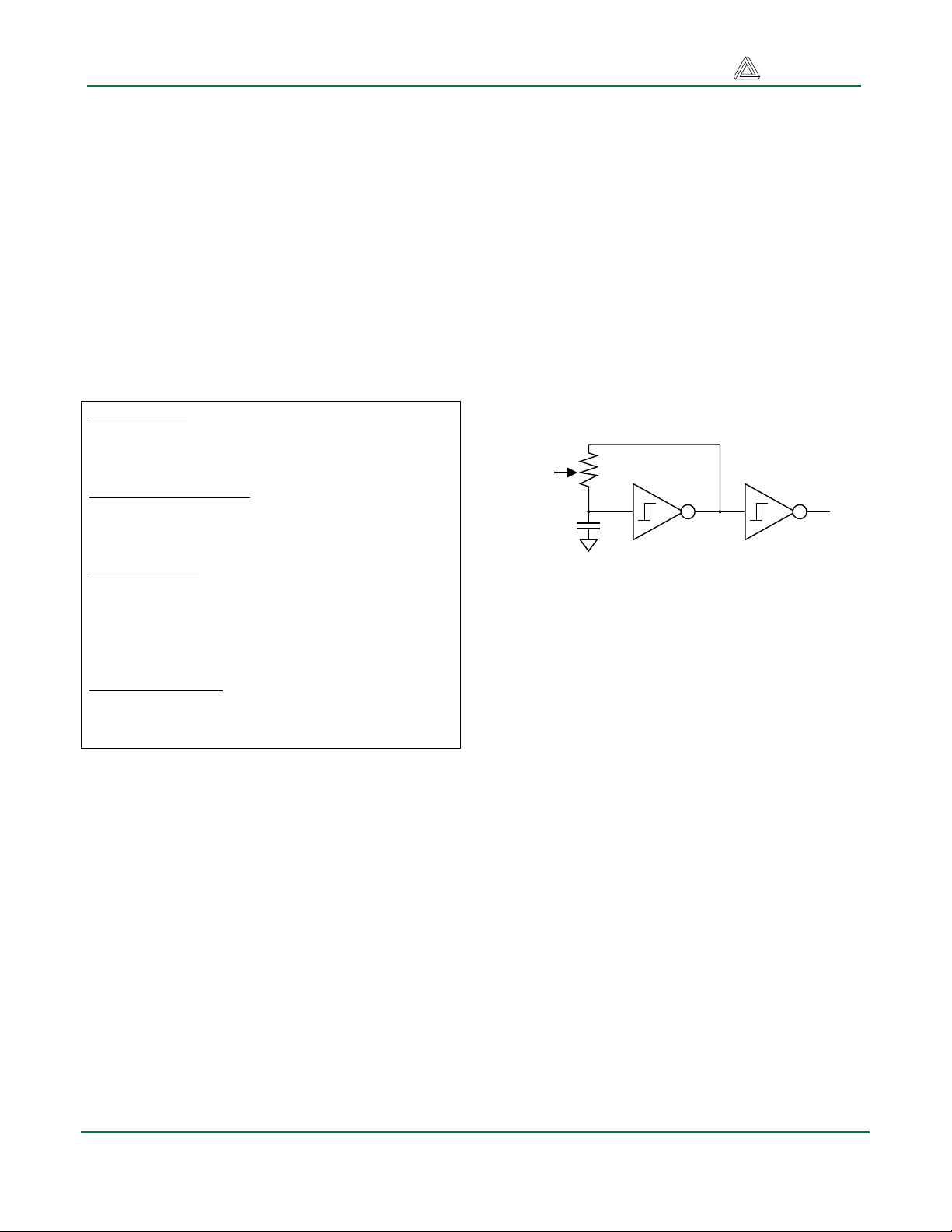
Oscillator
The XCRP board provides an user-adjustable
oscillator that can produce a clock signal in the
0.5 to 4KHz range. The oscillator circuit uses
an auto-feedback Schmidt-trigger inverter, with
a variable resistor and fixed 4.7uF capacitor in
the feedback path. The variable resistor is a
User
Adjust
MCLK
Figure 2. Oscillator Circuit
15-turn precision potentiometer that can be
adjusted from 0 to 500K ohms, providing an
RC time constant that varies by several orders
of magnitude. This clock source provides an
adequate frequency range for experiments that
Table 1. XCRP board signal definitions
CPLD configuration circuit
The XCRP board uses a JTAG port connector
to route programming signals from a host
computer to the CPLD. The programming
circuit simply connects the JTAG port pins
driven by the Xilinx CAD tools directly to the
CPLD programming pins, making the board
fully compatible with all Xilinx programming
tools. To configure the board from a computer
using the JTAG cable, ensure the circuit is
powered either by batteries or by an external
power supply. Before running Xilinx’s iMPACT
programmer tool to download a bit file, ensure
that the JTAG start-up clock is selected in the
run from “human time” (i.e., less than 1 Hz) to
the audio range. The oscillator output drives
the CLK0 input of the CPLD via a second
Schmidt trigger.
Power Supplies
The XCRP board can be powered from any
wall-plug transformer that uses a 2.1mm
center-positive jack, and that produces at least
100mA in the 5VDC to 9VDC range. The board
can also be powered from 2AA cells or any
other power source that outputs at least
100mA at 2.5 to 4.0 volts. The secondary
power source connector bypasses the onboard regulators, so if that connector is used,
ensure that no more than 4VDC is applied to
the board. During operation, the board
“Generate Programming File” properties dialog
Copyright Digilent, Inc. Page 2/2 Doc: 502-046
Page 3

XCRP Reference Manual Digilent, Inc.
n
r
consumes less than 80mA with all LEDs and
LED segments illuminated.
LEDs
Eight LEDs (four red, two yellow, and two
green) are provided for circuit outputs. LED
anodes are driven directly from the CPLD via
470-ohm resistors, and the cathodes are
connected directly to ground. The CPLD
Slide Switches
Eight slide switches are provided for circuit
inputs. The slide switches use a 4.7Kohm
series resistor for nominal input protection.
Switch outputs are available at the expansion
connector.
connection point is also available at the
expansion connector via a 470-ohm resistor.
Three colors are offered so that circuits like
traffic light controllers or basic meters can
easily be implemented. A ninth LED is also
provided as a power-on LED.
4.7K
ohms
To CPLD &
expansion
connector
From
CPLD
Expansion
Connector
470
ohms
470
ohms
Figure 5. Slide Switch Circuit
Seven Segment Display
The XCRP board contains a modular 2-digit,
common cathode, seven-segment LED
Figure 3. LED Circuit
Pushbutton
Four debounced pushbuttons are provided for
circuit inputs. Buttons are debounced with an
RC-Schmidt trigger circuit so that they may be
used as clocks for basic sequential circuits.
Button outputs (at the output of the Schmidt
trigger) are normally low, and they are driven
high only when the button is pressed. Button
outputs are available at the expansion
connector.
display. In a common cathode display, the
seven cathodes of the LEDs forming each digit
are connected to a common circuit node.
On the XCRP board, the two-digit display has
two common cathode nodes labeled CAT1 and
CAT2. Both cathodes, and therefore both
digits, can be independently turned on and off
by driving the CAT1/2 signals to a ‘1’ or a ‘0’
respectively.
The anodes of similar segments on both
displays are also connected together into
seven common circuit nodes labeled AA
through AG. Thus, each anode for both
displays can be turned on and off
independently. This connection scheme
creates a multiplexed display, where driving
0.1uF
4.7K ohms
4.7K ohms
To CPLD
expansio
connecto
the cathode signals and corresponding anode
patterns of each digit in a repeating,
continuous succession can create a stable 2digit display.
Even though each digit is illuminated only half
Figure 4. Pushbutton Circuit
time, the human eye will be “tricked” into
seeing continuously illuminated digits (this
Copyright Digilent, Inc. Page 3/3 Doc: 502-046
Page 4

XCRP Reference Manual Digilent, Inc.
phenomenon is used by all multiplexed
displays, including televisions, computer
monitors, and motion pictures). To appear
bright and continuously illuminated, both digits
should be driven once every 1 to 16ms (for a
refresh frequency of 1KHz to 60Hz). For
example, in a 60Hz refresh scheme, each digit
would be illuminated for ½ of the refresh cycle,
or 8ms.
A display controller must assure that the
correct anode pattern is present when the
illustrate the process, if CAT1 is driven high
while AB and AC are driven high, then a “1” will
be displayed in digit position 1. Then, if CAT2
is driven high while AA, AB and AC are driven
high, then a “7” will be displayed in digit
position 2. If ACAT1/AB, AC are driven for
8ms, and then CAT2/AA, AB, AC are driven for
8ms in an endless succession, the display will
show “17” and the observer cannot tell that
both digits are not continuously illuminated. An
example timing diagram is provided below.
corresponding cathode signal is driven. To
afgedcb
Common
cathode
(a) (b)
Figure 7. (a ) Seven segm e nt display de ta i l.
( b) comm o n c a t hode displ a y conf i gurat ion.
(c) segement illumination patterns for decimal
digits . (d) segment illumination truth table.
Refresh peri od = 1 t o 16m s
Di gi t peri od = Ref res h / 2
CAT1
Digit
Shown
0
1
2
3 1 1 1 1 0 0 1
4
5 1 0 1 1 0 1 1
6
7 1 1 1 0 0 0 0
8
9 1 1 1 1 0 1 1
(c)
Illuminated Segment
a b c d e f g
1 1 1 1 1 1 0
0 1 1 0 0 0 0
1 1 0 1 1 0 1
0 1 1 0 0 1 1
1 0 1 1 1 1 1
1 1 1 1 1 1 1
(d)
Anodes connect ed t o CP LD and ex pansion
connector via 470- ohm resis tors
aa ab ac ad ae af ag
470
470
CAT2
Anodes
Digit1 Digit2 Digit3 Digit4
Di agram show i ng timing requirements
The seven-segment display anodes are driven
from the CPLD pins via 470 resistors, and the
cathodes are driven by two 2N3904 NPN
transistors to supply the required cathode
CAT1 CAT2
100
Cathodes connec t ed to ground vi a tw o transi stors
driv en f rom the C P LD and t he expans i on connec t or
CPLD via 100-ohm resistors. The CPLD
connection point is also available at the
expansion connector via a 470-ohm resistor.
current. The 3904 bases are driven from the
Copyright Digilent, Inc. Page 4/4 Doc: 502-046
Page 5

XCRP Reference Manual Digilent, Inc.
Expansion connector
An expansion connector labeled J3 on the
board edge has been provided so that designs
can easily be extended beyond the XCRP
board. The connector uses a 2 x 20, 100-mil
spaced grid so that standard headers or
sockets may easily be loaded (no expansion
connector is loaded during manufacturing to
allow greater flexibility). All available CPLD
signals are routed to the connector, including
CPLD
The Xilinx CoolRunner XCR3064 CPLD on the
XCRP board uses a 44-pin PLCC package,
with four used for VCC connections, three for
GND, and five for JTAG programming. All
remaining 32 I/O pins are routed to the
expansion connector, and 31 are also routed to
on-board devices (4 for pushbuttons, 8 for slide
switches, 8 for LEDs, 10 for the seven-
segment device and one for the system clock).
signals that drive on-board devices. Where
feasible, on-board devices are decoupled from
the CPLD with series resistors so that all pins
may be used as inputs or outputs by the
expansion connector. VCC and GND are also
routed to the connector so that attached
devices can draw power from the XCRP board.
Xilinx
XCR3064
CoolRunner
CPLD
Clock
LEDs
7-seg
display
Table 2. Digilab XCR board expansion
connector pinout
Pin Signal Pin Signal Pin Signal Pin Signal
1 GND 11 SW4 21 AD 31 NC
2 NC 12 LED5 22 BTN2 32 SW5
3 VCC 13 NC 23 AC 33 NC
4 LED1 14 LED6 24 BTN3 34 SW6
5 SW1 15 AG 25 AB 35 NC
6 LED2 16 LED7 26 BTN4 36 SW7
7 SW2 17 AF 27 AA 37 NC
8 LED3 18 LED8 28 CAT1 38 SW8
9 SW3 19 AE 29 NC 39 NC
10 LED4 20 BTN1 30 CAT2 40 IO1
Push
buttons
Slide
switches
4
8
8
10
32
Expansion
Connector
Figure 7. CPLD Connections
The block diagram shows all connections
between the CPLD and the devices on the
board. CPLD pin connections are shown in the
following table.
Table 3. Digilab XCR board CPLD pinout
in Signal Pin Signal Pin Signal Pin Signal
BTN1
MCLK
BTN4
SW4
0
PORTEN
1
VCC
SW1
SW2
TDI
SW3
IO1
12
13
14
15
16
17
18
19
20
21
22
SW8
TMS
SW7
VCC
SW6
SW5
CAT1
CAT2
IO2
AG
GND
23 VCC 34
24 AF 35
25 AE 36
26 AD 37
27 AC 38
28 AB 39
29 AA 40
30 GND 41
31 LED8 42
32 TCK 43
33 LED6 44
LED7
VCC
LED5
LED4
TDO
LED3
LED2
LED1
GND
BTN3
BNT2
The CPLD device can be configured using the
Xilinx JTAG tools and a JTAG programming
cable connecting the XCRP board and the host
computer. A Xilinx programming cable can also
be used.
The XCRP board can also accommodate a
XCR3032 CPLD. For further information on the
CoolRunner CPLD, please see the Xilinx data
sheets available at the Xilinx website
(www.xilinx.com).
Copyright Digilent, Inc. Page 5/5 Doc: 502-046
 Loading...