

Page 1
DDiiggiilleenntt VViiddeeoo DDeeccooddeerr BBooaarrdd
TM
((VVDDEECC11)) RReeffeerreennccee MMaannu
Revision: 4/12/05
uaall
Overview
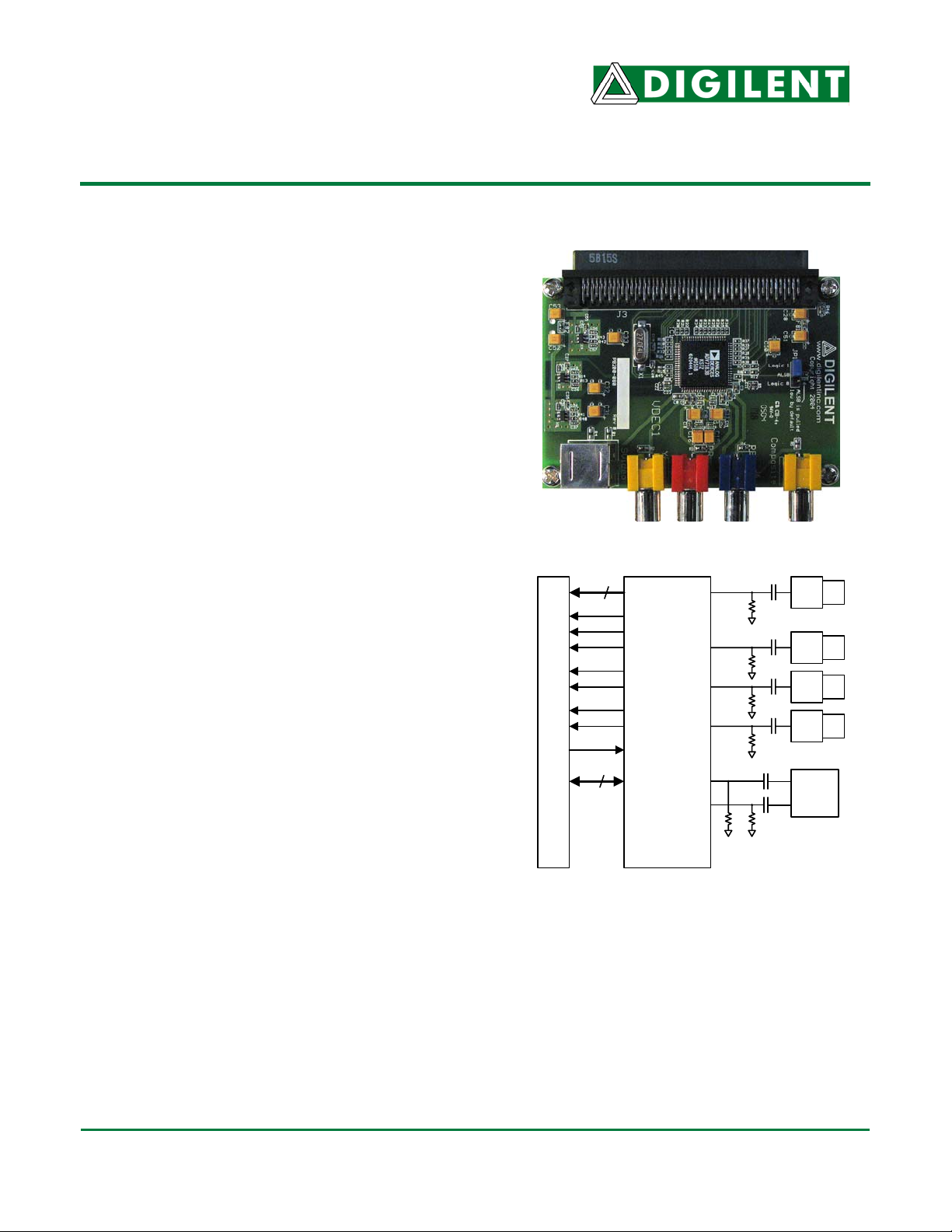
The Video Decoder 1 board (VDEC1),
centered on the ADV7183B Video Decoder
chip from Analog Devices, can digitize NTSC,
PAL, and SECAM video signals. The
ADV7183B automatically detects standard
analog baseband television signals, and
digitizes them with three 54MHz 10-bit ADCs.
Output data can be sent to an attached system
board in 8-bit or 16-bit YCrCb 4:2:2 format.
Features include:
• component, composite, and S-video
inputs;
2C®
• I
compatible control bus;
• high-speed Hirose FX2 data connector
• supports NTSC, PAL, and SECAM
inputs
• 8-bit or 16-bit YCrCb 4:2:2 outputs plus
HS, VS and Field signals
• programmable controls include peak
white, hue, brightness, saturation and
contrast.
Functional Description
The VDEC1 board is essentially a “carrier” for
Analog Devices’ ADV7183B Video Decoder
chip. It contains all required support circuitry,
including well-filtered and stable power
supplies, properly terminated75-ohm inputs, a
stable 27-MHz clock source, various video
input connectors, and input protection
networks. Refer to the Analog Devices data
sheet for more information about the
ADV7138B.
The VDEC1 can be used with any Digilent
board that uses the Hirose FX2 connector.
Catalog entries in the Digilent products
webpage contain a “connector” field that
www.digilentinc.com
246 East Main | Pullman, WA 99163
(509) 334 6306 Voice and Fax
75
75
75
75
.1uF
Yel
.1uF
Blu
.1uF
Red
.1uF
Grn
.1uF
S
Video
75
16
2
Data
CVBS
HS
VS
Field
LLC1
LLC2
INTRQ
SFL
OE
uWIRE/
I2C
Analog
Devices
ADV7183B
PB
PR
SV_Y
SV_C
Y
VEDC1 Circuit Diagram
clearly shows which boards have the Hirose
connector.
Operation
In operation, the VDEC1 should not be
attached to a system board until the signals
driving the Hirose connector from the system
board have been properly defined. If the
Copyright Digilent, Inc. 2 pages Doc: 502-04 6
Page 2
VDEC1 Reference Manual
VDEC1 board is attached to a system board,
and the system board is driving as outputs the
same signals the VDEC1 is driving, damage to
the VDEC1 and system board will result.
Before attaching the VDEC1 to a system
board, ensure that any power-on autoloaded configuration drives the Hirose pins
correctly. Otherwise, ensure the system
board powers on in a reset mode, not
driving the Hirose pins as outputs.
Once the VDEC1 board is attached to a
system board, the ADV7183B chip must be
programmed (via its I
2C®
compatible port) for a
specific operating mode before output video
data is available. Please refer to the
ADV7138B data sheet for information on
programming various operation modes.
After an operating mode has been selected, a
video source can be attached to the
appropriate video input connector, and output
digital video data will be available.
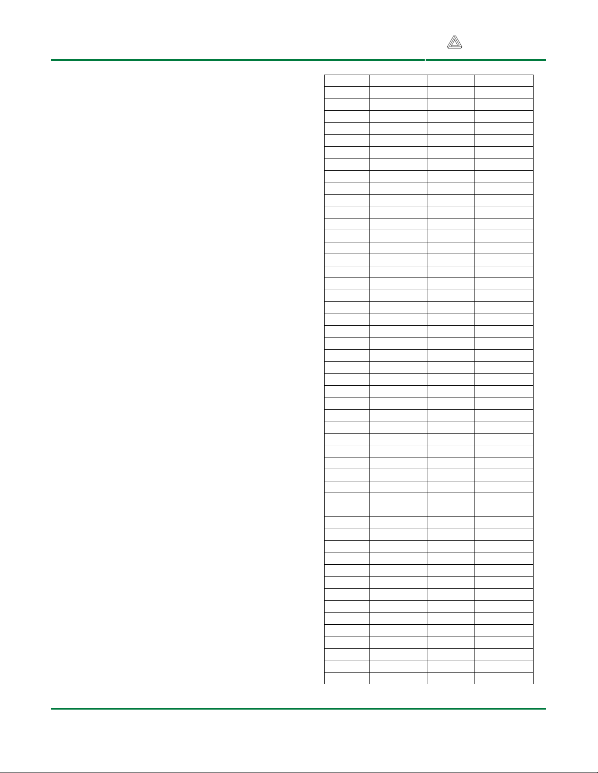
Hirose Connector Pinout
The VDEC1 contains a 100-pin Hirose FX2
socket connector that mates with a
corresponding Hirose plug connector on a
system board. Pin1 of the socket connector
attaches to pin1 of the plug connector. Thus, to
generate a pin connection list for a given
system board, the signal definitions in the
following table can be directly mapped to the
signal definitions on the system board (e.g.,
the signal name on VDEC1 pin5 maps directly
to the signal on the system board pin5).
Digilent, Inc.
www.digilentinc.com
A Pin # Signal B Pin # Signal
1 VCC33 1 Shield
2 VCC33 2 GND
NC
NC
NC
NC
NC
NC
NC
NC
NC
NC
NC
NC
NC
NC
NC
3 NC
4 NC
5 GND
GND
GND
GND
GND
GND
GND
GND
GND
GND
GND
GND
GND
GND
GND
GND
GND
GND
GND
GND
GND
GND
GND
GND
GND
GND
GND
GND
GND
34
35
36
37
38
39
40
41
42
43
44
45
GND
GND
GND
GND
GND
GND
GND
GND
GND
GND
GND
GND
GND
GND
3
4
5
6 RESET 6
7 SDA 7
8 SCLK 8
9 P15 9
10 P14 10
11 P13 11
12 P12 12
13 OE 13
14 FIELD 14
15 VS 15
16 HS 16
17 P11 17
18 P10 18
19 P9 19
20 P8 20
21 INTRQ 21
22 SFL 22
23 P7 23
24 P6 24
25 P5 25
26 P4 26
27 P3 27
28 P2 28
29 LLC2 29
30 P1 30
31 P0 31
32 PWRDN 32
33 NC 33
34
35
36
37
38
39
40
41
42
43
44
45
46 GND 46
47 NC 47
48 GND 48 NC
49 VCC5 49 VCC5
50 VCC5 50 Shield
Copyright Digilent, Inc. Page 2/2 Doc: 502-046
 Loading...