

Page 1
PPmmooddGGYYRROO22™™ RReeffeerreennccee MMaannuuaal
l
Revision: October 24, 2012
Note: This document applies to REV A of the board.
Overview
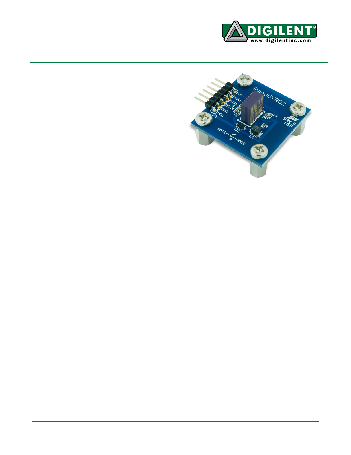
The PmodGYRO2 features the Analog Devices
ADXRS453 High Performance, Digital Output
Gyroscope that is ideal for systems in need of
a gyroscope for high vibration environments.
Functional Description
The PmodGYRO2 is a single-axis high
performance gyroscope that utilizes a standard
6-pin connector and communicates via a Serial
Peripheral Interface (SPI) bus.
Interface
The PmodGYRO2 interfaces with systems
using standard SPI transmission protocol. (See
table 1 for signal descriptions.) The module is
set up for Clock Phase = Clock Polarity = 0 or
SPI mode 0. Users should drive SPI
communication only to a maximum frequency
of 8MHz.
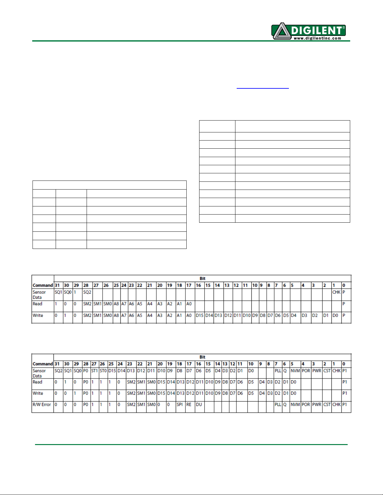
This Analog Devices gyroscope utilizes a 32bit Command/Response system to facilitate
communication with user devices. System
commands are sent to the Pmod during one
32-bit transmission sequence, and it returns a
response during the next 32-bit transmission
sequence. This message layout ensures that
the very first module response is always
0x00000001. (See table 2 for details on bit
definitions.)
When users assert chip select for each
command, the PmodGyro2 begins latching rate
data in case the command is a data request.
The device then sends the data via the
response in the next command sequence. The
PmodGyro2 is capable of sending three
different types of command packets and
returning four different response packets. (See
tables 3 and 4 for a breakdown of the allowed
SPI commands and responses.)
Even though commands are 32-bits wide and
the data part is 16-bits wide, each register in
1300 NE Henley Court, Suite 3
Pullman, WA 99163
(509) 334 6306 Voice | (509) 334 6300 Fax
Features include:
• Simple SPI interface
• ±300°/sec angular rate sensing
• Ultrahigh vibration rejection .01°/sec/g
• Excellent 16°/hour null bias stability
• Internal temperature compensation
• Continuous self-test
the device is only 8-bits wide. Due to the
differences in widths, a read command will
return the register requested and the next
sequential register in the memory map. The
same width ratio applies to a write command.
Users should address read and write
commands to even registers only. Users
that desire access to an odd register must
address commands to the previous (even)
register.
For simple acquisition of data, users should
issue an SPI Command in the Sensor Data
Format. This will return an SPI Response in
the Sensor Data Format on the next SPI
transmission.
The ADXRS453 has a continuous self-test
function that tests the complete
electromechanical system and reports errors to
the user. The ADXRS453 returns results to
users via the FAULT register. The status of
the PmodGYRO2 is included in most
responses The PmodGyro2 also prevents
Doc: 502-232 page 1 of 2
Page 2
PmodGYRO2 Reference Manual
Bits
Description
Connector J1
Pin Signal
Description
temporary spikes in data from causing a failing
status response by filtering raw data from the
self-test before sending a pass/fail status. The
module stores both the raw data and the
filtered data in the HICSTx and LOCSTx
registers. Users may access this data should
they be concerned about these energy spikes.
The temperature sensor data is useful for
temperature compensation of the rate data and
is also directly available to the user. To get the
temperature sensor data users must simply
execute a read command of the TEMx
registers from the device.
Table 1: Interface Connector Signal
Description
1 CS Chip Select
2 MOSI Master Out/Slave In
3 MISO Master In/Slave Out
4 SCLK Serial Clock
5 GND Power Supply Ground
6 VCC Power Supply (3.3v)
Note: For more information on the GYRO2
module interface, see the ADXRS453
datasheet available online from Analog
Devices at www.analog.com.
Table 2: SPI Bit Definitions
SQ[2:0] Sequence bits
SM[2:0] Sensor module bits (always 0b000)
A[8:0] Register address
D[15:0] Data
P Command odd parity
SPI SPI command/response error
RE Request Error
DU Data Unavailable
ST[1:0] Status Bits
P0 Response, odd parity, Bits[31:16]
P1 Response, odd parity, Bits[31:0]
Table 3: SPI Commands
Table 4: SPI Responses
www.digilentinc.com page 2 of 2
Copyright Digilent, Inc. All rights reserved. Other product and company names mentioned may be trademarks of their respective owners.
 Loading...