

Page 1
DDiiggiilleenntt PPeeggaassuuss BBooaarrdd
RReeffeerreennccee MMaannuuaal
Revision: August 11, 2005 215 E Main Suite D | Pullman, WA 99163
l
www.digilentinc.com™
(509) 334 6306 Voice and Fax
Overview
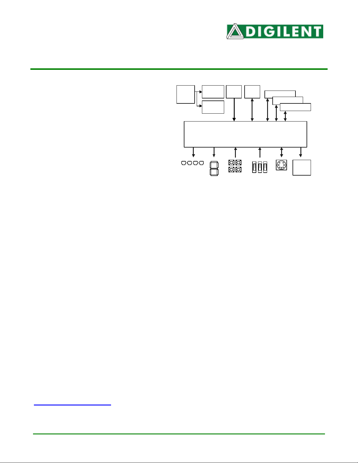
The Pegasus circuit board provides a complete
circuit development platform centered on a
Xilinx Spartan 2 FPGA. Pegasus features
include:
Power
jack
5-9VDC
2.5VDC
regulator
3.3VDC
regulator
Clock
(50MHz)
Config
ROM
Expansion Connectors
A1
A2
B1
JTAG
• a 50K-gate Xilinx Spartan 2 FPGA with
Xilinx Spartan 2 XC2S50-PQ208
50K gates and 200MHz operation (a
200K-gate version is also availabl e)
• a XCF01S Xilinx Platform Flash ROM
(XCF02S for 200K gate version)
• a collection of I/O devices including eight
LEDs, four-digit seven-segment display,
four pushbuttons, and eight slide
switches
• a 50MHz oscillator and a socket for a
8 LEDs
4 7-seg.
displays
4 buttons
8 switches
Figure 1. Pegasus circuit board block diagram
PS2
Port
VGA
Port
second oscillator
• PS/2 and VGA ports
• 96 I/O signals routed to three standard
40-pin expansion connectors
• all I/O signals have ESD and short-circuit
protection
• a JTAG programming port.
The Pegasus board has been designed to
work seamlessly with all versions of the Xilinx
ISE CA D tools, including the free WebPack
tools available from Xilinx. A growing collection
of low-cost expansion boards can be used with
the Pegasus board to add analog and digital
I/O capabilities, as well as various data ports
like Ethernet and USB. The Pegasus board
ships with a power supply and programming
cable, so designs can be implemented
immediately without the need for any additional
hardware.
Important: This reference manual is
updated for Rev. D Pegasus Boards with a
5V power supply. For a manual for a
previous Pegasus board using a 3.3V
power supply, e-mail
support@digilentinc.com
Functional Description
The Pegasus board provides an inexpensive,
robust, and easy -to-use platform that anyone
can use to gain experience with FPGA devices
and modern design methods. The Pegasus
board is centered on the Spartan 2 FPGA, and
it contains all needed support circuits so
designs can get up and running quickly. The
large collection of on -board I/O devices allows
many designs to be completed without the
need for any other components. Three
standard expansion connectors allow designs
to grow beyond the Pegasus board, either with
user-designed boards or any one of several
analog and digital I/O boards offered by
Digilent. Each expansion connector provides
system voltages and 32 unique I/O signals,
with all I/O signals protected against damage
from ESD and short-circuit connections. JTAG
signals are routed to two expansion
connectors, allowing peripheral boards to drive
the scan chain or to be configured along with
the Spartan FPGA. The collection of on-board
I/O devices and signal protection networks
make the Pegasus board ideally suited to
educational settings.
Copyright Digilent, Inc. All rights reserved 12 pages Doc: 50 0-223
Page 2
Pegasus Reference Manual Digilent, Inc. ™
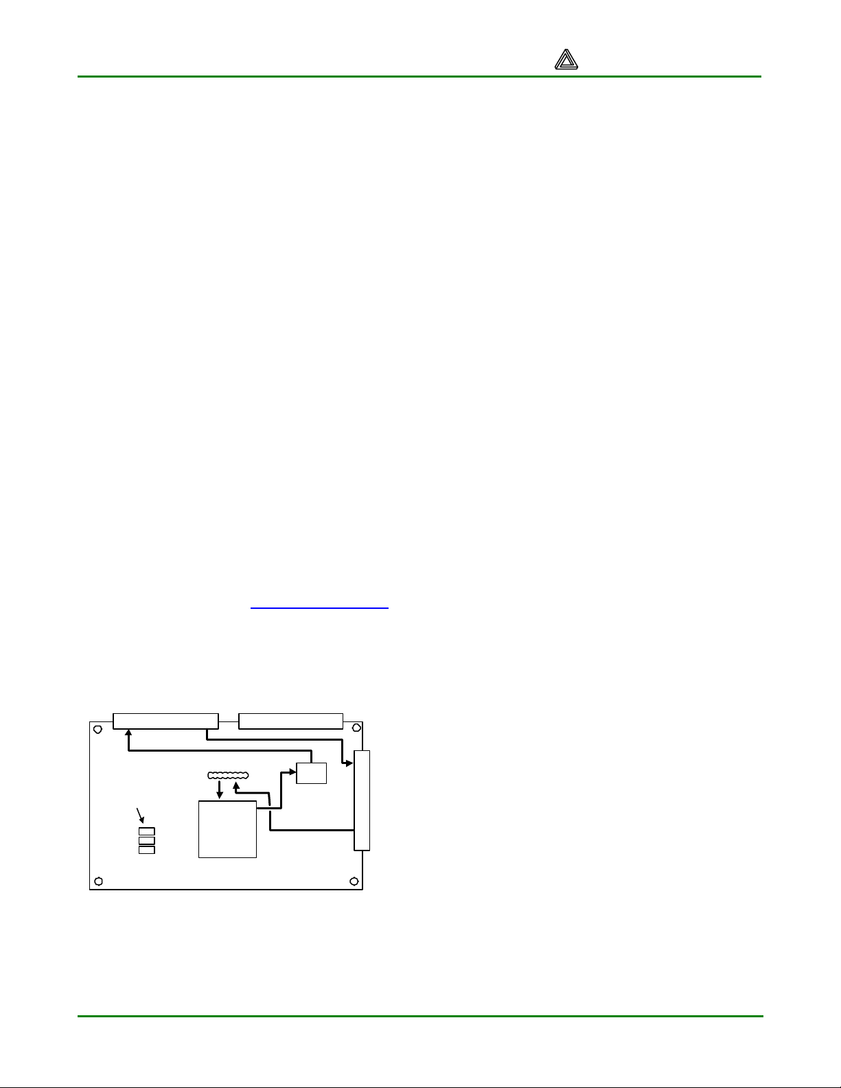
JTAG Ports and Device Configuration
The Spartan 2 FPGA, the XCF01S Platform
Flash ROM, and any programmable devices
on peripheral boards attached to the Pegasus
board can be programmed through JTAG
ports. The JTAG scan chain is routed from the
primary JTAG connector (port 1) to the FPGA,
Platform Flash, and two connection ports as
shown in Figure 2. The primary configuration
port (Port 1) uses a standard 6-pin JTAG
header (J6) that can accommodate Digilent’s
JTAG3 cable (or cables from Xilinx or other
vendors). The other two bi-directional JTAG
ports are available on the A1 and B1
expansion connectors. If no peripheral boards
are present on these connectors, a buffer on
the Pegasus board removes them from the
JTAG chain. If a peripheral board with a JTAGprogrammable device is attached, the scan
chain is driven out the expansion connector so
that the device can be configured. If a Digilent
port module is connected to A1 or B1, then the
port module can drive the JTAG chain to
program all devices in the scan chain. Port
modules include Ethernet, USB, EPP parallel,
and serial modules. (See www.digilentinc.com
for more information). For port modules to
drive the JTAG chain, a jumper must be
installed on the primary JTAG connector
across the TDI and TDO pins.
Port 2
A1 A2
Port 3
JTAG connector
Programming
mode select
jumpers
(Port 1)
Spartan 2E
PQ 208
Platform
Flash
B1
Figure 2. JTAG signal routing on Pegasus
To program the Pegasus board from the
primary port, first power on the Pegasus board,
then connect it to the PC with a JTAG cable,
and then run the “auto-detect” feature of the
configuration software. The configuration
software will identify all devices in the scan
chain, and then each device can be bypassed
or programmed with a suitable configuration
file. Note that both the FPGA and Platform
Flash ROM will always appear in the scan
chain. If the Platform Flash ROM is loaded with
an FPGA configuration file, the FPGA will load
that file at power-on if jumpers are loaded in all
three positions of J4 (M2, M1, and M0).
Power Supplies
The Pegasus board requires a regulated 5V
power supply (it ships with a 5V regulated wallplug supply). If a higher voltage supply is used,
the Pegasus board may be permanently
damaged. The power supply is connected to
the Pegasus board using a 5.5mm OD, 2.5mm
ID center-positive power jack. The 5V supply
from the power jack is connected directly to the
V
supply that drives the FPGA I/O signals,
CCIO
and to a 2.5V regulator that supplies the
Spartan 2 V
CORE
voltage.
Total board current is dependant on FPGA
configuration, clock frequency, and external
connections. In test circuits with roughly 20K
gates routed, a 50MHz clock source, and all
LEDs illuminated, approximately 200mA +/30% of supply current is drawn from the 2.5V
supply, and approximately 100mA is drawn
from the 5V supply. Required current will
increase if peripheral boards are attached.
The Pegasus board uses a four layer PCB,
with the inner layers dedicated to VCC and
GND planes. Most of the VCC plane is at 5V,
with an island under the FPGA at 2.5V. The
FPGA and the other ICs on the board all have
0.047uF bypass capacitors placed as close as
possible to each VCC pin. The power supply
routing and bypass capacitors result in a very
clean, low-noise power supply.
Oscillators
The Pegasus provides a 50MHz SMD primary
oscillator and a socket for a second oscillator.
www.digilentinc.com Page 2
Page 3
Pegasus Reference Manual Digilent, Inc. ™
The primary oscillator is connected to the
GLK1 input of the Spartan 2 (pin 77) and the
secondary oscillator is connected to GCLK2
(pin 182). Both clock inputs can drive a DLL on
the Spartan 2, allowing for a wide range if
internal frequencies are up to four times higher
than the external clock signals. Any 5V
oscillator in a half-size DIP package can be
loaded into the secondary oscillator socket.
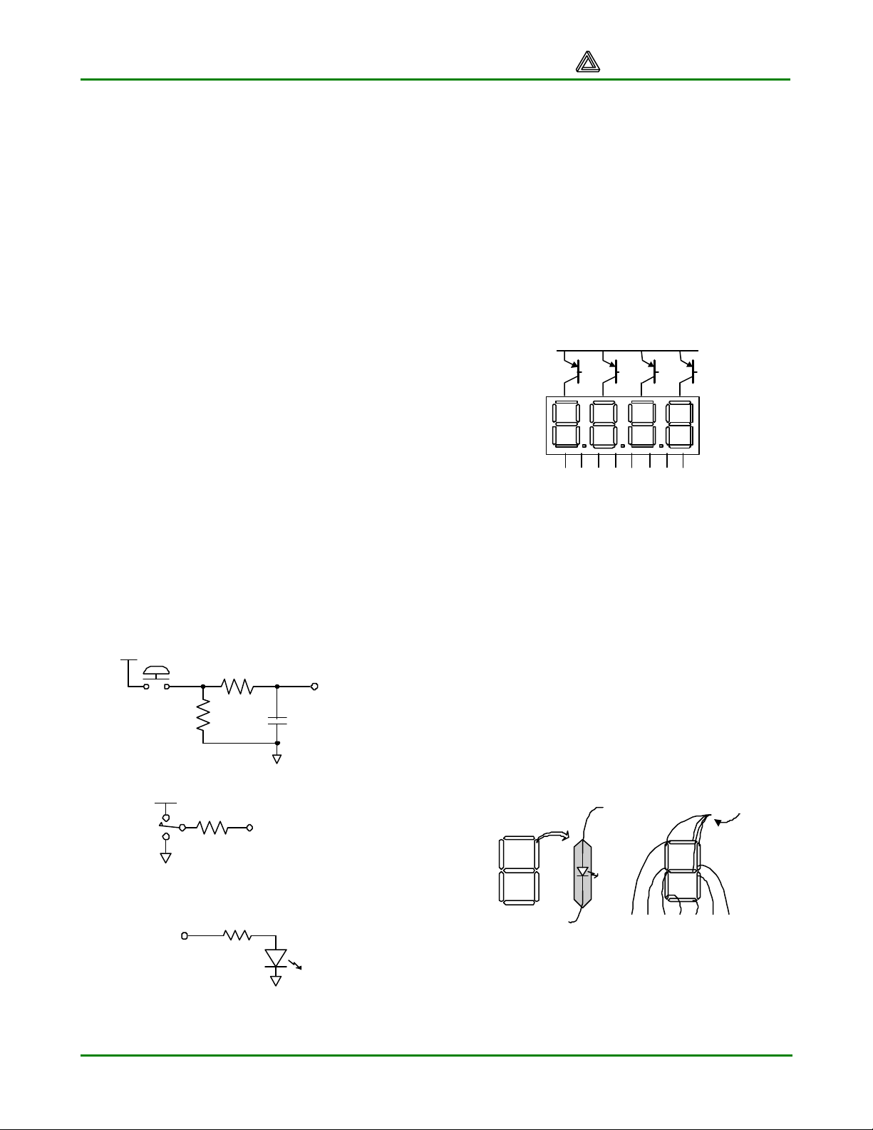
Pushbuttons, Slide Switches, and LEDs
Four pushbuttons and eight slide switches are
provided for circuit inputs. Pushbutton inputs
are normally low, and they are driven high only
when the pushbutton is pressed. Slide
switches generate constant high or low inputs
depending on their position. Pushbutton inputs
use RC networks to provide nominal debounce
and ESD protection. Slide switch inputs use
only a series resistor for protection.
Eight LEDs are provided for circuit outputs.
LED anodes are driven directly from the FPGA
via 470-ohm resistors, and the cathodes are
connected directly to ground. A ninth LED is
provided as a power-on LED, and a tenth LED
indicates JTAG programming status.
3.3V
4.7K ohms
To FPGA
4.7K
ohms
Pushbuttons
3.3V
4.7K
ohms
Slide switches
0.1uF
To FPGA
Seven-Segment Display
The Pegasus board contains a four-digit
common anode seven-segment LED display.
The display is multiplexed, so only seven
cathode signals exist to drive all 28 segments
in the display. Four digit-enable signals drive
the common anodes and these signals
determine which digit the cathode signals
illuminate.
Anodes are connected via
transistors for greater current
Vdd
AN0
AN1AN2AN3
abc d e f g dp
Cathodes are connected to
Xilinx device via 100Ω resistors
Figure 4. Common anode Sseg display
The seven anodes of each digit’s LEDs are
connected together into one “common anode”
circuit node. The display has four such nodes
named AN0 – AN3, and the signals that drive
these nodes serve as digit enablers. Driving an
anode signal low enables the corresponding
digit. The cathodes of similar segments on all
four displays are connected into seven circuit
nodes labeled CA through CG. Driving cathode
signals low illuminates segments on any digit
whose digit enable is low.
Common anode
a
f
e
b
g
c
From
FPGA
LEDs
Figure 3. Pushbutton, slide switch, and LED circuits
www.digilentinc.com Page 3
390 ohms
This connection scheme creates a multiplexed
display, where driving the anode signals and
corresponding cathode patterns of each digit in
d
a f g e d c b
Figure 5. Common anode detail
Page 4
Pegasus Reference Manual Digilent, Inc. ™
PS/2 Power
a repeating, continuous succession can create
the appearance of a four-digit display. Each of
the four digits will appear bright and
continuously illuminated if the digit enable
signals are driven low once every 1 to 16ms
(for a refresh frequency of 1KHz to 60Hz). For
example, in a 60Hz refresh scheme, each digit
would be illuminated for one quarter of the
refresh cycle, or 4ms. The controller must
assure that the correct cathode pattern is
present when the corresponding anode signal
is driven.
Refresh period = 1ms to 16ms
AN0
AN1
AN2
AN3
Digit 0
Digit period = Refresh / 4
Digit 1 Digit 2 Digit 3
Figure 6. Sseg signal timing
To illustrate the process, if AN0 is driven low
while CB and CC are driven low, then a “1” will
be displayed in digit position 0. Then, if AN1 is
driven low while CA, CB and CC are driven
low, then a “7” will be displayed in digit position
1. If AN0 and CB, CC are driven low for 4 ms,
and then AN1 and CA, CB, CC are driven low
for 4 ms in an endless succession, the display
will show “71” in the rightmost two digits.
Digit Cathode Signals
Shown
0
1 1 0 0 1 1 1 1
2
3
4
5
6
7
8
9
a b c d e f g
0 0 0 0 0 0 1
0 0 1 0 0 1 0
0 0 0 0 1 1 0
1 0 0 1 1 0 0
0 1 0 0 1 0 0
0 1 0 0 0 0 0
0 0 0 1 1 1 1
0 0 0 0 0 0 0
0 0 0 1 1 0 0
Figure 7. Cathode patterns for decimal digit s
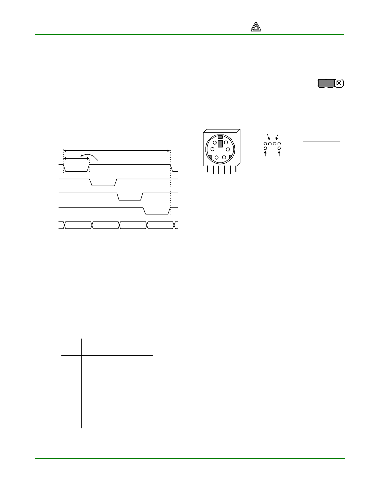
PS/2 Port
The Pegasus board includes a 6-pin mini-DIN
connector that can accommodate a PS/2
mouse or keyboard connection. A jumper on
the Pegasus board (J9) can be
loaded to provide 5V to the PS/2
J9
VCC33
PS2VCC
VU
port, or an external supply can be
connected to the “PS2VCC” pin of
J9 (some PS/2 devices require 5V
to work properly).
Pin Definitions
Pin Function
1 Data
2 Reserved
3 GND
4 Vdd
5 Clock
6 Reserved
1
2
4
PS2 Connector
3
6
5
Pin 1
Pin 2
Pin 5Pin 6
Bottom-up
hole pattern
Figure 8. PS/2 connections
The PS/2 protocol uses a bi-directional two wire interface that includes a serial data and a
clock signal (the host -to-keyboard data
direction is used to send status LED data).
Driver circuits on both ends of the clock and
data signals use open-collector buffers with
10K pull-ups. The signals are only driven when
a key is actively pressed (or when the host is
actively sending LED status data). If the PS/2
device is only used as an input device, then
the host system can just use input buffers
(open-collector buffers are not required).
PS/2 mouse and keyboard devices use11-bit
data words that include a start bit, eight data
bits, and odd parity bit, and a stop bit. Data
timings are shown in the figure below. The
mouse and keyboard use eight-bit data
packets that are organized differently – the
keyboard sends eight-bit key scan codes, and
the mouse sends three eight-bit data elements
to define relative mouse movements.
Keyboard
Each key has a single, unique scan code that
is sent whenever the corresponding key is
pressed. If a key is continuously pressed for
more than 570ms, its scan code is repeated
each 104ms (but the time interval between first
and second transmission of the same code is
www.digilentinc.com Page 4
Page 5

Pegasus Reference Manual Digilent, Inc. ™
570ms). When releasing a key that was
pressed for more than 570ms, an “F0” key-up
code is sent, followed immediately by the key
scan code. If a key can be “shifted” to produce
a new character (like a capital letter), then the
shift character is sent before the key scan
code. Some keys, called extended keys, send
an “E0” ahead of the scan code (and they may
send more than one scan code). When an
extended key is released, an “E0 F0” key-up
code is sent, followed by the scan code.
Signals timings and scan codes for most keys
are shown in the figure below.
A host device can also send data to the
keyboard. Below is a short list of some oftenused commands.
ED Set Num Lock, Caps Lock, and Scroll Lock
LEDs. After receiving an “ED”, the keyboard
returns an “FA”. Then the host sends a byte
to set LED status: bit 0 sets Scroll Lock, bit 1
sets Num Lock, and bit 2 sets Caps Lock.
Bits 3 to 7 are ignored.
EE Echo. Upon receiving an echo command, the
keyboard replies with “EE”.
F3 Set scan code repeat rate. The keyboard
acknowledges receipt of an “F3” by returning
an “FA”, after which the host sends a second
byte to set the repeat rate.
FE Resend. Upon receiving FE, the keyboard re -
sends the last scan code sent.
FF Reset. Resets the keyboard.
The keyboard should send data to the host
only when both the data and clock lines are
high (or idle). Since the host is the “bus
master”, the keyboard should check to see
whether the host is sending data before driving
the bus. To facilitate this, the clock line can be
used as a “clear to send” signal. If the host
pulls the clock line low, the keyboard must not
send any data until the clock is released.
Mouse
The mouse outputs a clock and data signal
when it is moved; otherwise, these signals
CLK
DATA
T
Edge 0
CK
'0 ' start bit '1 ' stop bit
T
CK
T
SU
T
HLD
Edge 10
Symbol Parameter Min Max
T
CK
Clock time
T
SU
Data-to-clock setup time
T
HLD Clock-to-data hold time 5us 25us
30us
5us
50us
25us
~3.1ms
Timing for a two-byte
scan code
Figure 9. PS/2 timings
~570ms
Scan code repeat timing
(key pressed and held)
~104ms
remain at logic ‘1’. Each time the mouse is
www.digilentinc.com Page 5
Page 6

Pegasus Reference Manual Digilent, Inc. ™
moved, three 11-bit words are sent from the
mouse to the host device. Each of the 11-bit
words contains a ‘0’ start bit, followed by eight
bits of data (LSB first), followed by an odd
parity bit, and terminated with a ‘1’ stop bit.
Thus, each data transmission contains 33 bits,
where bits 0, 11, and 22 are ‘0’ start bits, and
bits 10, 21, and 32 are ‘1’ stop bits. The three
8-bit data fields contain movement data as
shown below. Data is valid at the falling edge
of the clock, and the clock period is 20 to
30KHz.
The mouse assumes a relative coordinate
system wherein moving the mouse to the right
generates a positive number in the X field, and
moving to the left generates a negative
Mouse status byte X direction byte Y direction byte
L R 0 1 XSYS XY YY P X0 X1 X2 X3 X4 X5 X6 X7 P Y0 Y1 Y2 Y3 Y4 Y5 Y6 Y7 P1 0 1 00 11
Idle state
Start bit Stop bit
Start bit
Figure 10. PS/2 mouse data
number. Likewise, moving the mouse up
generates a positive number in the Y field, and
moving down represents a negative number
(the XS and YS bits in the status byte are the
sign bits – a ‘1’ indicates a negative number).
The magnitude of the X and Y numbers
represent the rate of mouse movement – the
larger the number, the faster the mouse is
moving (the XV and YV bits in the status byte
are movement overflow indicators – a ‘1’
means overflow has occurred). If the mouse
moves continuously, the 33-bit transmissions
are repeated every 50ms or so. The L and R
fields in the status byte indicate left and right
button presses (a ‘1’ indicates the button is
being pressed).
Stop bit
Start bit
Stop bit
Idle state
VGA Port
The five standard VGA signals red (R), green
(G), blue (B), horizontal sync (HS), and vertical
ync (VS) are routed from FPGA pins to the
VGA connector. The color signals pass
through 270-ohm resistors on the Pegasus
board to create a resistor-divider with the 75ohm VGA cable termination. This limits the
voltage at the VGA connector to the specified
0V (fully-off) to 0.7V (fully-on) range. This
three-bit color system allows for eight different
colors as shown in the table.
Color Red Green Blue
Black 0 0 0
Blue 0 0 1
Green 0 1 0
Cyan 0 1 1
Red 1 0 0
Purple 1 0 1
Yellow 1 1 0
White 1 1 1
Table 1. Three-bit color system
CRT Display Systems Background
Cathode ray tube (CRT)-based VGA displays
use amplitude-modulated, moving electron
beams (or cathode rays) to display information
on a phosphor-coated screen. LCD displays use
an array of switches that can impose a voltage
across a small amount of liquid crystal, thereby
changing light permittivity through the crystal on
a pixel-by-pixel basis. Although the following
description is limited to CRT displays, LCD
displays have evolved to use the same signal
timings as CRT displays (so the “signals”
discussion below pertains to both CRTs and
LCDs).
CRT displays use three electron beams (one for
red, one for blue, and one for green) to energize
the phosphor that coats the inner side of the
display end of a cathode ray tube (see drawing
below). Electron beams emanate from electron
guns, which are finely-pointed heated cathodes
placed in close proximity to a positively charged
annular plate called a “grid”.
www.digilentinc.com Page 6
Page 7

Pegasus Reference Manual Digilent, Inc. ™
The electrostatic force imposed by the grid
pulls away rays of energized electrons as
current flows into the cathodes. These cathode
rays are initially accelerated towards the grid,
but they soon fall under the influence of the
much larger electrostatic force that results from
the entire phosphor-coated display surface of
the CRT being charged to 20kV (or more). The
particle rays are focused to a fine beam as
they pass through the center of the grids, and
then they accelerate to impact on the
phosphor-coated display surface. The
phosphor surface glows brightly at the impact
point, and the phosphor continues to glow for
several hundred microseconds after the beam
is removed. The larger the current fed into the
cathode, the brighter the phosphor will glow.
Between the grid and the display surface, the
beam passes through the neck of the CRT
where two coils of wire produce orthogonal
electromagnetic fields. Because cathode rays
are composed of charged particles (electrons),
they can be deflected by these magnetic fields.
Current waveforms are passed through the
coils to produce magnetic fields that interact
with the cathode rays and cause them to
transverse the display surface in a “raster”
pattern, horizontally from left to right and
vertically from top to bottom.
As the cathode ray moves over the surface of
the display, the current sent to the electron guns
can be increased or decreased to change the
brightness of the display at the cathode ray
impact point. Information is only displayed when
the beam is moving in the “forward” direction (left
to right and top to bottom), and not during the
time the beam is reset back to the top left edge
of the display. Much of the potential display time
is therefore lost in “blanking” periods when the
beam is reset and stabilized to begin a new
horizontal or vertical display pass.
The size of the beams, the frequency at which
the beam can be traced across the display, and
the frequency at which the electron beam can be
modulated determine the display resolution.
Modern VGA displays can accommodate
different resolutions, and a VGA controller circuit
dictates the resolution by producing timing
signals to control the raster patterns. The
controller must produce synchronizing pulses at
5V to set the frequency at which current flows
through the deflection coils, and it must ensure
that video data is applied to the electron guns at
the correct time.
Raster video displays define a number of “rows”
that corresponds to the number of horizontal
passes the cathode makes over the display area,
and a number of “columns” that corresponds to
an area on each row that is assigned to one
“picture element” or pixel. Typical displays use
Anode (entire screen)
Cathode ray tube
Deflection coils
Cathode ray
Cathode ray tube display system
Grid
Electron guns
(Red, Blue, Green)
R,G,B signals (to guns)
gun
deflection
control
High voltage supply (>20kV) Control board
www.digilentinc.com Page 7
grid
control
control
Sync signals
(to deflection control)
VGA cable
Page 8

Pegasus Reference Manual Digilent, Inc. ™
from 240 to 1200 rows, and from 320 to 1600
columns. The overall size of a display, and the
number of rows and columns determines the
size of each pixel.
Video data typically comes from a video
refresh memory, with one or more bytes
assigned to each pixel location (the DIO4
board uses three bits per pixel). The controller
must index into video memory as the beams
move across the display, and retrieve and
apply video data to the display at precisely the
time the electron beam is moving across a
given pixel.
VGA System Timing
VGA signal timings are specified, published,
copyrighted, and sold by the VESA
organization (www.vesa.org). The following
VGA system timing information is provided as
an example of how a VGA monitor might be
driven in 640 by 480 mode. For more precise
information, or for information on higher VGA
frequencies, refer to the VESA website above.
A VGA controller circuit must generate the HS
and VS timing signals and coordinate the
delivery of video data based on the pixel clock.
The pixel clock defines the time available to
display one pixel of information. The VS signal
defines the “refresh” frequency of the display,
i.e., the frequency at which all information on
the display is redrawn. The minimum refresh
frequency is a function of the display’s phosphor
and electron beam intensity, with practical
refresh frequencies falling in the 50Hz to 120Hz
range.
The number of lines to be displayed at a given
refresh frequency defines the horizontal “retrace”
frequency. For a 640-pixel by 480 -row display
using a 25MHz pixel clock and 60 +/-1Hz
refresh, the signal timings shown in the table
below can be derived. Timings for sync pulse
width and front and back porch intervals (porch
intervals are the pre- and post -sync pulse times
during which information cannot be displayed)
are based on observations taken from VGA
displays.
A VGA controller circuit decodes the output of a
horizontal-sync counter driven by the pixel clock
to generate HS signal timings. This counter can
be used to locate any pixel location on a given
row. Likewise, the output of a vertical-sync
counter that increments with each HS pulse can
be used to generate VS signal timings, and this
counter can be used to locate any given row.
These two continually running counters can be
used to form an address into video RAM. No
time relationship between the onset of the HS
pulse and the onset of the VS pulse is specified,
so the designer can arrange the counters to
easily form video RAM addresses, or to minimize
Symbol Parameter
T
Sync pulse time
S
T
Display time
disp
p
T
Pulse width
w
T
Front porch
fp
T
Back porch
bp
Horizontal
Counter
Vertical Sync
Time Clocks Lines
16.7ms
15.36ms
320 us
928 us
Zero
Detect
3.84us
Detect
64 us
416,800
384,000
1,600
8,000
23,200
Set
Horizontal
Synch
Reset
521
480
2
10
29
Horizontal Sync
Time
25.6 us
3.84 us
640 ns
1.92 us
Clocks
32 us
800
640
96
16
48
CE VS
Vertical
Counter
p
T
w
Zero
Detect
64us
Detect
T
S
T
disp
Reset
Set
Vertical
Synch
T
fp
T
bp
HS
www.digilentinc.com Page 8
Page 9

Pegasus Reference Manual Digilent, Inc. ™
decoding logic for sync pulse generation.
Expansion Connectors
40-Pin Connectors
Three expansion connectors labeled A1, A2,
and B1 are available on the Pegasus board.
These female so cket connectors mate with
100-mil spaced, 2x20 right-angle headers
(available at most distributors). All three
connectors have GND on pin 1, VU on pin 2,
and 5V on pin 3. Pins 4-35 route to FPGA I/O
signals, and pins 36-40 are reserved for JTAG
and/or clock signals (see Figure 13).
Each of the expansion connectors provides 32
unique I/0 signals. These signals have been
grouped into three different types of busses for
documentation purposes, and to facilitate
communications with external boards. The
lower 18 pins (pins 4-21) of the A1 and B1
connectors are designated as the “system
bus”. The system bus defines eight data
signals, six address lines, two strobes (WE and
USB or Ethernet boards) use the module bus.
Module bus timings are consistent with EPP bus
timings.
6-Pin Connector
The Pegasus board also contains a 6-pin
accessory port (J1). This port provides Vdd,
GND, and four unique FPGA signals. Several 6pin module boards that can attach to this
connector are available from Digilent, including
speaker boards, H -bridge boards, sensor
boards, etc.
Peripheral Bus
System Bus
The “system bus” is a protocol used by certain
expansion boards that mimics a simple 8-bit
microprocessor bus. It includes eight data lines,
six address lines, a write-enable (WE) strobe
that can be used by the peripheral to latch
written data, an output-enable (OE) strobe that
can be used by the peripheral to enable read
Figure 7. Expansion Connector Pins
OE), a chip select, and a clock. The lower 18
pins of the A2 connector are designated as the
“peripheral bus”, and the individual pins are not
assigned any further definitions. The upper 14
pins of each expansion connector (pins 22-35)
have been designated as “module busses”.
Module bus pin definitions are consistent with
enhanced parallel port (EPP) pin definitions,
and they include eight address/data lines,
three strobes (address write, data write, and
read/write), and three status lines (wait, reset,
and initialize). Figure 13 below shows
expansion connector signal routing. Some
Digilent peripheral boards use the system bus
pins. Bus timings mimic a simple 8-bit
microprocessor bus, with signal timings shown
in figure 14 below. Module boards (like the
Pin 4
Pin 1: GND
Pin 2: VU
Pin 39
Pin 40
Pin 3: 3.3V
data, a chip select, and a clock to enable
synchronous transfers. Figure 14 shows bus
signal timings used by Digilent to create bus
controllers in peripheral devices. However, any
bus and timing model can be used by modifying
circuits in the FPGA and attached peripheral
devices.
Module Bus
The module bus protocol is used by various
module boards (like the Ethernet and U SB
modules) to communicate with the Pegasus
board. The module bus signals and timings are
borrowed from the EPP protocol. Timings and
signals are shown here.
www.digilentinc.com Page 9
Page 10

Pegasus Reference Manual Digilent, Inc. ™
System Bus Timing
Symb
ol
ten Time to enable after CS asserted 10ns
th Hold time 1ns
tdoe Time to disable after OE de-
asserted
teoe Time to enable after OE asserted 15ns
tw Write strobe time 10ns
tsu Data setup time 5ns
twd Write disable time 0ns
Parameter Time
(typ)
10ns
Write Cycle
Ten
CS
Tdoe
OE
Tw
WE
Tsu
DB0-DB7
Th
Teoe
Th
Module Bus Timing
Symb
Parameter Time
ol
tstb Strobe time 10ns
twt Strobe to wait time 10 ns
twr Time to enable write 15 ns
tsu Data setup time 5 ns
th Data hold time 5 ns
Write Cycle*
ASTB
DSTB
WAIT
nWR
T
STB
T
STB
T
WT
T
WR
T
H
T
H
(typ)
Read Cycle
CS
OE
WE
DB0-DB7
Twd
Tsu
Read data latch time
ThTen
TdoeTeoe
Th
Th
DATA
Read Cycle*
ASTB
DSTB
WAIT
nWR
DATA
Figure 14. Peripheral bus signals and timings
* ASTB and DSTB determine whether an address or
data write cycle occurs. Only one should be
asserted for each bus transaction.
T
SU
T
STB
T
STB
T
WT
T
WR
Tsu
T
H
T
H
T
H
Th
www.digilentinc.com Page 10
Page 11

Pegasus Reference Manual Digilent, Inc. ™
Pegasus Expansion Connector Pinout
Connector B1 Connector A1 Connector A2
Pin Signal B1 Pin Signal A1 Pin Signal A2
39 TDO TDO 39 TDO TDO 39 GCK0 GCK0
40 TDI TDI 40 TDI TDI 40 GND GND
37 TMS TMS 37 TMS TMS 37 n/c n/c
38 TCK TCK 38 TCK TCK 38 n/c n/c
35 MB1-INIT 90 35 MA1-INIT 189 35 MA2-INT 138
36 GND GND 36 GND GND 36 Not used n/c
33 MB1-WAIT 95 33 MA1-WAIT 192 33 MA2-WAIT 140
34 M1-RST 94 34 M1-RST 191 34 MA2-RST 139
31 MB1-DSTB 97 31 MA1-DSTB 194 31 MA2-DSTB 142
32 MB1-WRIT 96 32 MA1-WRIT 193 32 MA2-WRIT 141
29 MB1-DB7 99 29 MA1-DB7 199 29 MA2-DB7 147
30 MB1-ASTB 98 30 MA1-ASTB 195 30 MA2-ASTB 146
27 MB1-DB5 101 27 MA1-DB5 201 27 MA2-DB5 149
28 MB1-DB6 100 28 MA1-DB6 200 28 MA2-DB6 148
25 MB1-DB3 108 25 MA1-DB3 203 25 MA2-DB3 151
26 MB1-DB4 102 26 MA1-DB4 202 26 MA2-DB4 150
23 MB1-DB1 110 23 MA1-DB1 205 23 MA2-DB1 160
24 MB1-DB2 109 24 MA1-DB2 204 24 MA2-DB2 152
21 P-LSBCLK 112 21 LSBCLK 3 21 P-IO18 162
22 MB1-DB0 111 22 MA1-DB0 206 22 MA2-DB0 161
19 P1-DB7 114 19 DB7 5 19 P-IO16 164
20 P-CSA 113 20 CSA 4 20 P-IO17 163
17 P-DB6 119 17 DB6 7 17 P-IO14 166
18 P-OE 115 18 OE 6 18 P-IO15 165
15 P-DB5 121 15 DB5 9 15 P-IO12 168
16 P-WE 120 16 WE 8 16 P-IO13 167
13 P-DB4 123 13 DB4 14 13 P-IO10 173
14 P-ADR5 122 14 ADR5 10 14 P-IO11 172
11 P-DB3 126 11 DB3 16 11 P-IO8 175
12 P-ADR4 125 12 ADR4 15 12 P-IO9 174
9 P-DB2 129 9 DB2 18 9 P-IO6 178
10 P-ADR3 127 10 ADR3 17 10 P-IO7 176
7 P-DB1 133 7 DB1 21 7 P-IO4 180
8 P-ADR2 132 8 ADR2 20 8 P-IO5 179
5 P-DB0 135 5 DB0 23 5 P-IO2 187
6 P-ADR1 134 6 ADR1 22 6 P-IO3 181
3 VCCO VCCO 3 VCCO VCCO 3 VCCO VCCO
4 P-ADR0 136 4 ADR0 24 4 P-IO1 188
1 GND GND 1 GND GND 1 GND GND
2 VU VU 2 VU VU 2 VU VU
Pin Name FPGA Pin Pin Name FPGA Pin
1 AC0 P49 4 AC3 P47
2 AC1 P48 5 GND 3 AC2 P81 6 Vdd -
Accessory Port Pinout
www.digilentinc.com Page 11
Page 12

Pegasus Reference Manual Digilent, Inc. ™
LD5
Pegasus FPGA Pin Assignments
Pin Function Pin Function Pin Function Pin Function
1 GND 53 VCCO 105 VCCO 157 TDO
2 TMS 54 MODE2 106 PROGRAM 158 GND
3 LLSBCLK 55 PB-IO14 107 INIT/IO 159 TDI
4 LCSA 56 PB-IO13 108 LMB1-DB3 160 LMA2-DB1
5 LDB7 57 BTN2 109 LMB1-DB2 161 LMA2-DB0
6 LOE 58 BTN1 110 LMB1-DB1 162 LPA-IO18
7 LDB6 59 BTN0 111 LMB1-DB0 163 LPA-IO17
8 LWE 60 AN0 112 LPB-LSBCLK 164 LPA-IO16
9 LDB5 61 CE 113 LPB-CSA 165 LPA-IO15
10 LADR5 62 CD 114 LPB-DB7 166 LPA-IO14
11 GND 63 DP 115 LPB-OE 167 LPA-IO13
12 VCCO 64 GND 116 GND 168 LPA-IO12
13 VCCINIT 65 VCCO 117 VCCO 169 GND
14 LDB4 66 VCCINIT 118 VCCINIT 170 VCCO
15 LADR4 67 CC 119 LPB-DB6 171 VCCINIT
16 LDB3 68 CG 120 LPB-WE 172 LPA-IO11
17 LADR3 69 AN1 121 LPB-DB5 173 LPA-IO10
18 LDB2 70 CB 122 LPB-ADR5 174 LPA-IO9
19 GND 71 AN2 123 LPB-DB4 175 LPA-IO8
20 LADR2 72 GND 124 GND 176 LPA-IO7
21 LDB1 73 CF 125 LPB-ADR4 177 GND
22 LADR1 74 CA 126 LPB-DB3 178 LPA-IO6
23 LDB0 75 AN3 127 LPB-ADR3 179 LPA-IO5
24 LADR0 76 VCCINIT 128 VCCINIT 180 LPA-IO4
25 GND 77 GCK1 129 LPB-DB2 181 LPA-IO3
26 VCCO 78 VCCO 130 VCCO 182 GCK2
27 VS 79 GND 131 GND 183 GND
28 VCCINT 80 GCK0 132 LPB-ADR2 184 VCCO
29 HS 81 SW7/AC2 133 LPB-DB1 185 GCK3
30 BLUE 82 SW6 134 LPB-ADR1 186 VCCINIT
31 GRN 83 SW5 135 LPB-DB0 187 LPA-IO2
32 GND 84 SW4 136 LPB-ADR0 188 LPA-IO1
33 RED 85 GND 137 GND 189 LMA1-INT
34 PS2C 86 SW3 138 LMA2-INT 190 GND
35 PS2D 87 SW2 139 LMA2-RESET 191 LMA1-RESET
36 LD7 88 SW1 140 LMA2-WAIT 192 LMA1-WAIT
37 LD6 89 SW0 141 LMA2-WRITE 193 LMA1-WRITE
38 VCCINIT 90 LMB1-INT 142 LMA2-DSTB 194 LMA1-DSTB
39 VCCO 91 VCCINIT 143 VCCINIT 195 LMA1-ASTB
40 MC1-DB4 92 GND 144 VCCO 196 VCCINIT
41
42 LD4 94 LMB1-RESET 146 LMA2-ASTB 198 GND
43 LD3 95 LMB1-WAIT 147 LMA2-DB7 199 LMA1-DB7
44 LD2 96 LMB1-WRITE 148 LMA2-DB6 200 LMA1-DB6
45 LD1 97 LMB1-DSTB 149 LMA2-DB5 201 LMA1-DB5
46 LD0 98 LMB1-ASTB 150 LMA2-DB4 202 LMA1-DB4
47 AC3 99 LMB1-DB7 151 LMA2-DB3 203 LMA1-DB3
48 AC1 100 LMB1-DB6 152 LMA2-DB2 204 LMA1-DB2
49 AC0 101 LMB1-DB5 153 DIN/D0/IO 205 LMA1-DB1
50 MODE1 102 LMB1-DB4 154 BTN3 206 LMA1-DB0
51 GND 103 GND 155 CCLK 207 TCK
52 MODE0 104 DONE 156 VCCO 208 VCCO
93 GND 145 GND 197 VCCO
www.digilentinc.com Page 12
 Loading...