

Page 1

DDiiggiilleenntt PPaarraalllleell IInntteerrffaaccee MMooddeell
RReeffeerreennccee MMaannuuaal
Revision: 08/10/2004
l
www.digilentinc.com
246 East Main | Pullman, WA 99163
(509) 334 6306 Voice and Fax
Introduction
The Digilent Communications Interface DLL, dpcutil.dll, provides a set of API functions for applications
programs running on a Microsoft Windows based computer to exchange data with logic implemented
in a Digilent system board. Various Digilent applications programs, such as Transport component of
the Adept Suite, depend on the data interchange API functions in dpcutil. The operation of these
functions depends on the presence of a Digilent communications subsystem component running the
appropriate firmware and the implementation of the appropriate interface logic in the gate array. This
document describes the functional requirements of the communications interface logic and provides a
sample implementation.
The logic described in this document implements are set of registers in the gate array. An application
on the host PC exchanges data with the design in the gate array by reading or writing these registers.
Digilent Communications Interface modules implement the interface described in this document to
control the reading and writing of these registers.
Functional Description
The Digilent Port Interface is patterned after the EPP mode of the parallel port interface on an IBM PC
type computer. This interface provides an 8 bit bi-directional parallel data bus and six handshaking
lines to control the data transfer. The actual data transfer speed that can be achieved depends on the
particular communications subsystem and firmware version being used.
The parallel port interface is made up of an eight bit wide address register and a set of eight bit wide
data registers. The address register holds the address of the data register currently being accessed.
Access to the registers is accomplished via transfer cycles. The four types of transfer cycles allowed
are: address read, address write, data read, and data write. Address read and address write cycles
read from or write to the address register. Data read and data write cycles read or write the data
register whose address is currently held in the address register.
The address register can be implemented with any number of bits up to the maximum size of eight
bits. Since the maximum size of the address register is eight bits, the maximum number of data
registers that can be implemented is 256. It isn’t necessary to implement all 256 possible data
registers. Only the registers needed for a particular application need to be implemented. It is
necessary for the application program using the interface to know which data registers are
implemented and what functions the implemented data registers perform.
Signal Descriptions
In the following description, the term host represents the host PC running the dpcutil application.
Signals sourced by the host are generated by the Digilent communication interface and are inputs to
the logic in the gate array. The term peripheral refers to the logic implemented in the gate array of the
system board. Signals sourced by the peripheral are outputs from the logic implemented in the gate
array.
The following signals make up the interface:
Name Source Description
DB0 – DB7 bidir Data bus. The host is the source during write cycles and the
peripheral is the source during read cycles.
WRITE host Transfer direction control. High = read, Low = write
Copyright Digilent, Inc. 11 pages Doc: 560-000
Page 2

Digilent Parallel Interface Model Digilent, Inc.
ASTB host Address strobe. Causes data to be read or written to the address
register
DSTB host Data strobe. Causes data to be read or written to a data register
WAIT peripheral Synchronization signal used to indicate when the peripheral is
read to accept data or has data available.
INT peripheral Interrupt. Used by the peripheral to interrupt the host to request
service. Not used by all Digilent communications subsystems.
RESET host Reset. Allows host to reset logic in the peripheral. Not currently
used by all Digilent communications subsystems.
Transfers from the host to the peripheral or from the peripheral to the host are accomplished using
one of four transfer bus cycles. The four possible bus cycles are: Address Read, Address Write, Data
Read, Data Write. The direction of the data transfer is controlled by the WRITE signal. If WRITE is
high (indicating a READ cycle) the peripheral is the source of the data and drives its data onto the
bidirectional data bus at the appropriate time in the cycle. If WRITE is low (indicating a WR ITE cycle)
the host is the source of the data and drives its data onto the bidirectional data bus. It is extremely
important that the peripheral logic in the gate array not drive data onto the data bus except during a
READ cycle. If the data bus is driven by the peripheral at incorrect times, it is possible to create bus
contention that can damage either the gate array or the communications subsystem. All bus cycles
are initiated and controlled by the host.
The WAIT signal is used to synchronize transfers between the host and the peripheral. The host will
not begin a transfer unless the wait signal is low. Once the host begins a bus cycle, it will hold the
strobe (either ASTB or DSTB) in the active state (prolonging the bus cycle) until WAIT goes high.
WAIT going high signals that the peripheral has completed its processing of the cycle. The host will
then bring the strobe to the inactive state completing the bus cycle. The peripheral then brings WAIT
low when it is ready for another transfer to begin.
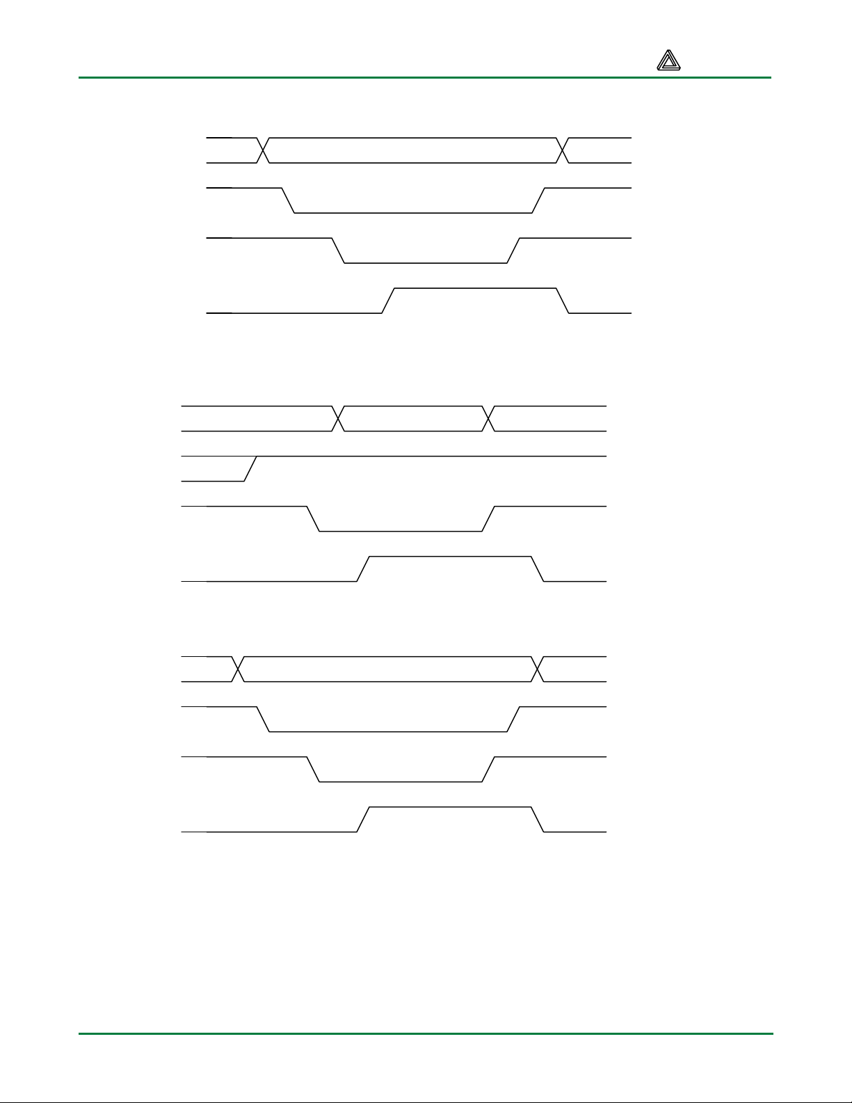
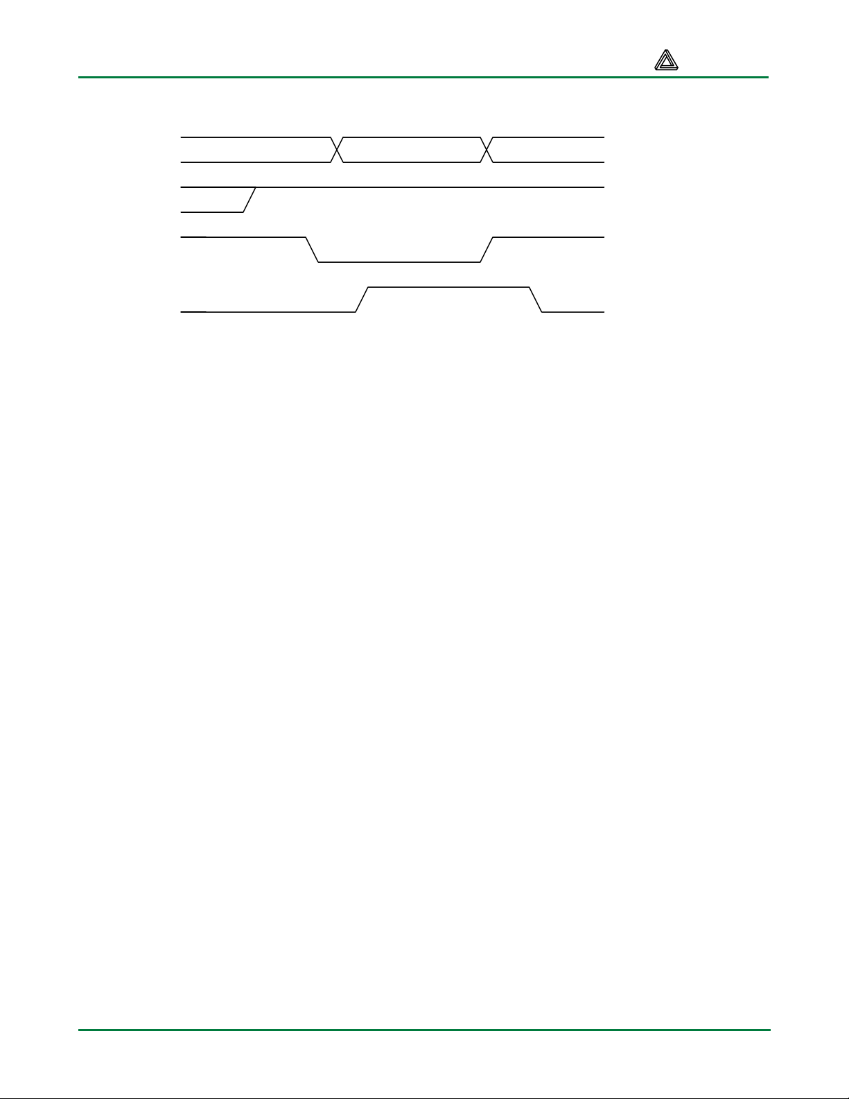
Timing Diagrams
The following diagrams illustrate the signal timing for the various transfer cycles. For write
cycles, the rising edge of the strobe signal (ASTB or DSTB) is the active edge and causes
the data to be latched into the register in the gate array. For read cycles, the WRITE signal
and the appropriate strobe are combined to enable to bus buffers to drive data onto the bus
when it is a read cycle and the strobe is active.
WAIT must be in the inactive state (low) before the communications module will start a
transfer cycle. The communications module will not complete a transfer cycle until WAIT goes
high. The gate array logic may delay bringing WAIT high to until data is available if
necessary. However, if WAIT is not brought high within approximately 10ms of the start of a
transfer, the communications module will abort the transfer and report a time out error back to
the host. Similarly if WAIT does not come low to allow a transfer to begin within
approximately 10ms, the communications module will report a time out error to the host.
www.digilentinc.com Copyright Digilent, Inc. Page 2
Page 3
Digilent Parallel Interface Model Digilent, Inc.
Address Write
DB
WRITE
ASTB
WAIT
Address Read
DB
WRITE
ASTB
WAIT
Data Write
DB
WRITE
DSTB
WAIT
www.digilentinc.com Copyright Digilent, Inc. Page 3
Page 4
Digilent Parallel Interface Model Digilent, Inc.
Data Read
DB
WRITE
DSTB
WAIT
www.digilentinc.com Copyright Digilent, Inc. Page 4
Page 5

Digilent Parallel Interface Model Digilent, Inc.
Example Source Code:
The following is an example of the interface implemented in VHDL.
----------------------------------------------------------------------------
-- DPIMREF.VHD -- Digilent Parallel Interface Module Reference Design
----------------------------------------------------------------------------
-- Author: Gene Apperson
-- Copyright 2004 Digilent, Inc.
----------------------------------------------------------------------------
-- This module contains an example implementation of Digilent Parallel
-- Interface Module logic. This interface is used in conjunction with the
-- DPCUTIL DLL and a Digilent Communications Module (USB, EtherNet, Serial)
-- to exchange data with an application running on a host PC and the logic
-- implemented in a gate array.
--
-- See the Digilent document, Digilent Parallel Interface Model Reference
-- Manual (doc # 560-000) for a description of the interface.
--
-- This design uses a state machine implementation to respond to transfer
-- cycles. It implements an address register, 8 internal data registers
-- that merely hold a value written, and interface registers to communicate
-- with a Digilent DIO4 board. There is an LED output register whose value
-- drives the 8 discrete leds on the DIO4. There are two input registers.
-- One reads the switches on the DIO4 and the other reads the buttons.
--
-- Interface signals used in top level entity port:
-- mclk - master clock, generally 50Mhz osc on system board
-- pdb - port data bus
-- astb - address strobe
-- dstb - data strobe
-- pwr - data direction (described in reference manual as WRITE)
-- pwait - transfer synchronization (described in reference manual
-- as WAIT)
-- rgLed - LED outputs to the DIO4
-- rgSwt - switch inputs from the DIO4
-- ldb - led gate signal for the DIO4
-- rgBtn - button inputs from the DIO4
-- btn - button on system board (D2SB or D2FT)
-- led - led on the system board
--
----------------------------------------------------------------------------
-- Revision History:
-- 06/09/2004(GeneA): created
-- 08/10/2004(GeneA): initial public release
----------------------------------------------------------------------------
library IEEE;
use IEEE.STD_LOGIC_1164.ALL;
use IEEE.STD_LOGIC_ARITH.ALL;
use IEEE.STD_LOGIC_UNSIGNED.ALL;
-- Uncomment the following lines to use the declarations that are
-- provided for instantiating Xilinx primitive components.
--library UNISIM;
--use UNISIM.VComponents.all;
entity dpimref is
www.digilentinc.com Copyright Digilent, Inc. Page 5
Page 6

Digilent Parallel Interface Model Digilent, Inc.
Port (
mclk : in std_logic;
pdb : inout std_logic_vector(7 downto 0);
astb : in std_logic;
dstb : in std_logic;
pwr : in std_logic;
pwait : out std_logic;
rgLed : out std_logic_vector(7 downto 0);
rgSwt : in std_logic_vector(7 downto 0);
rgBtn : in std_logic_vector(4 downto 0);
btn : in std_logic;
ldg : out std_logic;
led : out std_logic
);
end dpimref;
architecture Behavioral of dpimref is
------------------------------------------------------------------------
-- Component Declarations
------------------------------------------------------------------------
------------------------------------------------------------------------
-- Local Type Declarations
------------------------------------------------------------------------
------------------------------------------------------------------------
-- Constant Declarations
------------------------------------------------------------------------
-- The following constants define state codes for the EPP port interface
-- state machine. The high order bits of the state number give a unique
-- state identifier. The low order bits are the state machine outputs for
-- that state. This type of state machine implementation uses no
-- combination logic to generate outputs which should produce glitch
-- free outputs.
constant stEppReady : std_logic_vector(7 downto 0) := "0000" & "0000";
constant stEppAwrA : std_logic_vector(7 downto 0) := "0001" & "0100";
constant stEppAwrB : std_logic_vector(7 downto 0) := "0010" & "0001";
constant stEppArdA : std_logic_vector(7 downto 0) := "0011" & "0010";
constant stEppArdB : std_logic_vector(7 downto 0) := "0100" & "0011";
constant stEppDwrA : std_logic_vector(7 downto 0) := "0101" & "1000";
constant stEppDwrB : std_logic_vector(7 downto 0) := "0110" & "0001";
constant stEppDrdA : std_logic_vector(7 downto 0) := "0111" & "0010";
constant stEppDrdB : std_logic_vector(7 downto 0) := "1000" & "0011";
------------------------------------------------------------------------
-- Signal Declarations
------------------------------------------------------------------------
-- State machine current state register
signal stEppCur : std_logic_vector(7 downto 0) := stEppReady;
signal stEppNext : std_logic_vector(7 downto 0);
signal clkMain : std_logic;
-- Internal control signales
signal ctlEppWait : std_logic;
www.digilentinc.com Copyright Digilent, Inc. Page 6
Page 7

Digilent Parallel Interface Model Digilent, Inc.
signal ctlEppAstb : std_logic;
signal ctlEppDstb : std_logic;
signal ctlEppDir : std_logic;
signal ctlEppWr : std_logic;
signal ctlEppAwr : std_logic;
signal ctlEppDwr : std_logic;
signal busEppOut : std_logic_vector(7 downto 0);
signal busEppIn : std_logic_vector(7 downto 0);
signal busEppData : std_logic_vector(7 downto 0);
-- Registers
signal regEppAdr : std_logic_vector(3 downto 0);
signal regData0 : std_logic_vector(7 downto 0);
signal regData1 : std_logic_vector(7 downto 0);
signal regData2 : std_logic_vector(7 downto 0);
signal regData3 : std_logic_vector(7 downto 0);
signal regData4 : std_logic_vector(7 downto 0);
signal regData5 : std_logic_vector(7 downto 0);
signal regData6 : std_logic_vector(7 downto 0);
signal regData7 : std_logic_vector(7 downto 0);
signal regLed : std_logic_vector(7 downto 0);
signal cntr : std_logic_vector(23 downto 0);
------------------------------------------------------------------------
-- Module Implementation
------------------------------------------------------------------------
begin
------------------------------------------------------------------------
-- Map basic status and control signals
------------------------------------------------------------------------
clkMain <= mclk;
ctlEppAstb <= astb;
ctlEppDstb <= dstb;
ctlEppWr <= pwr;
pwait <= ctlEppWait; -- drive WAIT from state machine output
-- Data bus direction control. The internal input data bus always
-- gets the port data bus. The port data bus drives the internal
-- output data bus onto the pins when the interface says we are doing
-- a read cycle and we are in one of the read cycles states in the
-- state machine.
busEppIn <= pdb;
pdb <= busEppOut when ctlEppWr = '1' and ctlEppDir = '1' else "ZZZZZZZZ";
-- Select either address or data onto the internal output data bus.
busEppOut <= "0000" & regEppAdr when ctlEppAstb = '0' else busEppData;
rgLed <= regLed;
ldg <= '1';
-- Decode the address register and select the appropriate data register
busEppData <= regData0 when regEppAdr = "0000" else
regData1 when regEppAdr = "0001" else
regData2 when regEppAdr = "0010" else
www.digilentinc.com Copyright Digilent, Inc. Page 7
Page 8

Digilent Parallel Interface Model Digilent, Inc.
regData3 when regEppAdr = "0011" else
regData4 when regEppAdr = "0100" else
regData5 when regEppAdr = "0101" else
regData6 when regEppAdr = "0110" else
regData7 when regEppAdr = "0111" else
rgSwt when regEppAdr = "1000" else
"000" & rgBtn when regEppAdr = "1001" else
"00000000";
------------------------------------------------------------------------
-- EPP Interface Control State Machine
------------------------------------------------------------------------
-- Map control signals from the current state
ctlEppWait <= stEppCur(0);
ctlEppDir <= stEppCur(1);
ctlEppAwr <= stEppCur(2);
ctlEppDwr <= stEppCur(3);
-- This process moves the state machine to the next state
-- on each clock cycle
process (clkMain)
begin
if clkMain = '1' and clkMain'Event then
stEppCur <= stEppNext;
end if;
end process;
-- This process determines the next state machine state based
-- on the current state and the state machine inputs.
process (stEppCur, stEppNext, ctlEppAstb, ctlEppDstb, ctlEppWr)
begin
case stEppCur is
-- Idle state waiting for the beginning of an EPP cycle
when stEppReady =>
if ctlEppAstb = '0' then
-- Address read or write cycle
if ctlEppWr = '0' then
stEppNext <= stEppAwrA;
else
stEppNext <= stEppArdA;
end if;
elsif ctlEppDstb = '0' then
-- Data read or write cycle
if ctlEppWr = '0' then
stEppNext <= stEppDwrA;
else
stEppNext <= stEppDrdA;
end if;
else
-- Remain in ready state
stEppNext <= stEppReady;
end if;
-- Write address register
when stEppAwrA =>
www.digilentinc.com Copyright Digilent, Inc. Page 8
Page 9

Digilent Parallel Interface Model Digilent, Inc.
stEppNext <= stEppAwrB;
when stEppAwrB =>
if ctlEppAstb = '0' then
stEppNext <= stEppAwrB;
else
stEppNext <= stEppReady;
end if;
-- Read address register
when stEppArdA =>
stEppNext <= stEppArdB;
when stEppArdB =>
if ctlEppAstb = '0' then
stEppNext <= stEppArdB;
else
stEppNext <= stEppReady;
end if;
-- Write data register
when stEppDwrA =>
stEppNext <= stEppDwrB;
when stEppDwrB =>
if ctlEppDstb = '0' then
stEppNext <= stEppDwrB;
else
stEppNext <= stEppReady;
end if;
-- Read data register
when stEppDrdA =>
stEppNext <= stEppDrdB;
when stEppDrdB =>
if ctlEppDstb = '0' then
stEppNext <= stEppDrdB;
else
stEppNext <= stEppReady;
end if;
-- Some unknown state
when others =>
stEppNext <= stEppReady;
end case;
end process;
------------------------------------------------------------------------
-- EPP Address register
------------------------------------------------------------------------
process (clkMain, ctlEppAwr)
begin
if clkMain = '1' and clkMain'Event then
if ctlEppAwr = '1' then
regEppAdr <= busEppIn(3 downto 0);
end if;
www.digilentinc.com Copyright Digilent, Inc. Page 9
Page 10

Digilent Parallel Interface Model Digilent, Inc.
end if;
end process;
------------------------------------------------------------------------
-- EPP Data registers
------------------------------------------------------------------------
-- The following processes implement the interface registers. These
-- registers just hold the value written so that it can be read back.
-- In a real design, the contents of these registers would drive additional
-- logic.
-- The ctlEppDwr signal is an output from the state machine that says
-- we are in a 'write data register' state. This is combined with the
-- address in the address register to determine which register to write.
process (clkMain, regEppAdr, ctlEppDwr, busEppIn)
begin
if clkMain = '1' and clkMain'Event then
if ctlEppDwr = '1' and regEppAdr = "0000" then
regData0 <= busEppIn;
end if;
end if;
end process;
process (clkMain, regEppAdr, ctlEppDwr, busEppIn)
begin
if clkMain = '1' and clkMain'Event then
if ctlEppDwr = '1' and regEppAdr = "0001" then
regData1 <= busEppIn;
end if;
end if;
end process;
process (clkMain, regEppAdr, ctlEppDwr, busEppIn)
begin
if clkMain = '1' and clkMain'Event then
if ctlEppDwr = '1' and regEppAdr = "0010" then
regData2 <= busEppIn;
end if;
end if;
end process;
process (clkMain, regEppAdr, ctlEppDwr, busEppIn)
begin
if clkMain = '1' and clkMain'Event then
if ctlEppDwr = '1' and regEppAdr = "0011" then
regData3 <= busEppIn;
end if;
end if;
end process;
process (clkMain, regEppAdr, ctlEppDwr, busEppIn)
begin
if clkMain = '1' and clkMain'Event then
if ctlEppDwr = '1' and regEppAdr = "0100" then
regData4 <= busEppIn;
end if;
end if;
end process;
www.digilentinc.com Copyright Digilent, Inc. Page 10
Page 11

Digilent Parallel Interface Model Digilent, Inc.
process (clkMain, regEppAdr, ctlEppDwr, busEppIn)
begin
if clkMain = '1' and clkMain'Event then
if ctlEppDwr = '1' and regEppAdr = "0101" then
regData5 <= busEppIn;
end if;
end if;
end process;
process (clkMain, regEppAdr, ctlEppDwr, busEppIn)
begin
if clkMain = '1' and clkMain'Event then
if ctlEppDwr = '1' and regEppAdr = "0110" then
regData6 <= busEppIn;
end if;
end if;
end process;
process (clkMain, regEppAdr, ctlEppDwr, busEppIn)
begin
if clkMain = '1' and clkMain'Event then
if ctlEppDwr = '1' and regEppAdr = "0111" then
regData7 <= busEppIn;
end if;
end if;
end process;
process (clkMain, regEppAdr, ctlEppDwr, busEppIn)
begin
if clkMain = '1' and clkMain'Event then
if ctlEppDwr = '1' and regEppAdr = "1010" then
regLed <= busEppIn;
end if;
end if;
end process;
------------------------------------------------------------------------
-- Gate array configuration verification logic
------------------------------------------------------------------------
-- This logic will flash the led on the gate array. This is to verify
-- that the gate array is properly configured for the test. This is a
-- simple way to verify that the gate array actually got configured.
led <= btn or cntr(23);
process (clkMain)
begin
if clkMain = '1' and clkMain'Event then
cntr <= cntr + 1;
end if;
end process;
----------------------------------------------------------------------------
end Behavioral;
www.digilentinc.com Copyright Digilent, Inc. Page 11
 Loading...