

Page 1
DDiiggiilleenntt NNeexxyyss BBooaarrdd
RReeffeerreennccee MMaannuuaal
Revision: February 19, 2007 215 E Main Suite D | Pullman, WA 99163
l
www.digilentinc.com
(509) 334 6306 Voice and Fax
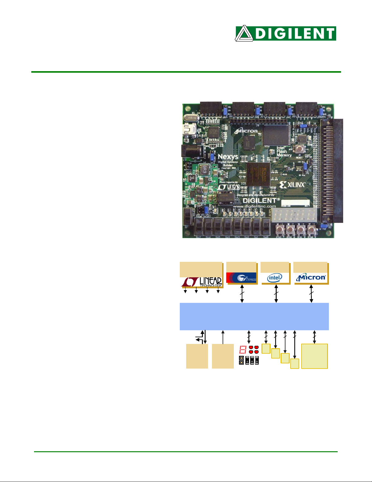
Overview
Digilent’s Nexys circuit board is an integrated
circuit development platform based on a Xilinx
Spartan 3 FPGA. The Nexys board provides
large external memory arrays, a collection of
useful I/O devices, and numerous ports,
making it an ideal platform for experiments
with FPGA-based digital systems, including
embedded cores like Xilinx’s MicroBlaze.
The Nexys board is suitable for designs
ranging from simple logic circuits to complex
digital systems, without needing any other
components. All external signals are ESD and
short-circuit protected, ensuring a long
operating life in any environment.
The Nexys is fully compatible with all versions
of the Xilinx ISE tools, including the free
WebPack. Nexys features include:
• 200K-gate Xilinx XC3S200 FPGA with
500+MHz operation (400K and 1M gate
versions available)
Switching
Power Supplies
USB2
Port
4Mbyte
Flash
16Mbyte
Cellular RAM
• USB2 port for FPGA configuration and
high-speed data transfers (using the free
3V3 1V2 2V5 1V8
32
32 32
Adept Suite Software)
• USB-powered (batteries and/or wall-plug
can also be used)
• 16MB of fast Micron PSDRAM and 4MB
of Intel StrataFlash Flash ROM
• Xilinx Platform Flash ROM that stores
FPGA configurations indefinitely
• High efficiency switching power supplies
(good for battery powered applications)
• 50MHz oscillator
• Connector for 1/8 VGA hi-res graphics
LCD panel or 16x2 character LCD display
JTAG
port
Platform
Flash
(config
ROM)
Xilinx Spartan3-200 FT256
-400 and -1000 FPGAs available
4 4 4 4
32
Clock
(100, 50,
or 25
MHz)
I/O devices
Figure 1: Nexys block diagram
JA
JB
JC
JD
43
High speed
100-pin
connector
• 60 FPGA I/O’s routed to expansion
connectors (one high-speed Hirose FX2 connector and four 6-pin headers)
• 8 LEDs, 4-digit seven-segment display, 4 pushbuttons, 8 slide switches
• Ships in a convenient plastic carry case (together with USB cable)
®
Copyright Digilent, Inc. All rights reserved 12 pages Doc: 502-107
Page 2

Nexys Reference Manual
Digilent
www.digilentinc.com
Functional Description
The Nexys board provides an inexpensive, robust, and easy-to-use platform that anyone can use to
gain experience with FPGA devices and modern design methods. It is centered on the Spartan 3
FPGA, and it contains all needed support circuits so designs can get up and running quickly. The
large collection of on-board devices allow many designs to be completed without the need for any
other hardware, making the Nexys an ideal platform for experimenting with new designs or learning
about FPGAs and CAD tools. The 100-pin high-speed connector and four 6-pin expansion connectors
allow designs to grow beyond the Nexys board, either with user-designed boards or breadboards
and/or peripheral module (Pmod) boards offered by Digilent. (Pmods are inexpensive analog and
digital I/O modules that offer A/D conversion, D/A conversion, motor drive, sensor input, and a host of
other features). Signals on each 6-pin expansion connector are protected against damage from ESD
and short-circuit connections, ensuring a long operating life in any environment. The Nexys board
works seamlessly with all versions of the Xilinx ISE tools, including the free WebPack tools. The
Nexys recieves power from the USB interface and it ships with a USB cable, so designs can be
implemented immediately without the need for any additional hardware.
FPGA and Platform Flash Configuration
The FPGA on the Nexys board must be configured (or programmed) by the user before it can perform
any functions. Design software, like the free WebPack from Xilinx, can be used to define any number
of circuits that can be programmed into the FPGA. Once programmed, the FPGA will retain its
configuration only as long is power is applied. The FPGA can be programmed in two ways: directly
from a PC, and from an on-board Platform Flash ROM that is also user-programmable. A jumper on
the Nexys board determines which source (PC or ROM) the FPGA will use to load its configuration.
The FPGA can automatically load a configuration at power-on from the Platform Flash ROM by setting
the Mode Select Jumper JP3 to “FLASH”.
Note that a demonstration configuration is loaded into the Nexys board during manufacturing. If that
configuration has not been overwritten, it can be automatically loaded into the FPGA by setting the
Mode Select Jumper JP3 to “FLASH”, and cycling power or pressing the reset button.
JTAG ROM
Configure from on-board ROM
Configure from PC via JTAG
JTAG3
header
XCF02
Platform
Flash
JTAG
Slave
Serial
Spartan 3
FPGA
Mode Select
Jumper
PROG
DONE
DONE
LED
Vdd
PROG
(reset)
button
Mode Select
Mode Select
Jumper
Jumper
JTAG3
header
DONE
LED
RESET
button
Copyright Digilent, Inc. Page 2/10 Doc: 502-107
Page 3
Nexys Reference Manual
Digilent
www.digilentinc.com
The FPGA and the Platform Flash ROM can be programmed from a PC using Digilent’s Adept
software or Xilinx’s iMPACT software (both are available for free download). Digilent’s Adept Software
works with the USB circuit, and Digilent’s JTAG3 parallel cable is compatible with iMPACT. When
using the USB circuit, a “cable bypass” jumper must be loaded on the JTAG header at J6 to connect
the TDI and TDO signals.
To program the Nexys board, connect the programming cable to the board and to a PC, and apply
power to the board. Start the programming software, and wait for the FPGA and the Platform Flash
ROM to be automatically identified. To program the FPGA, select the desired .bit file; to program the
Platform Flash, select the desired .mcs file. Right-click on the device to be programmed, and select
the “program” function. The configuration file will be sent to the FPGA or Platform Flash, and the
software will indicate whether programming was successful. For more information on device
programming, refer to the Adept or iMPACT reference manual.
Both the FPGA and Platform Flash ROM will always appear in the scan chain. After the Platform
Flash ROM has been loaded with a configuration file, the FPGA can automatically load that file at
power-on if programming mode control jumper is loaded in the ROM position.
A reset button is provided (labeled “reset”) that can erase the configuration in the FPGA, and start a
new programming cycle. An LED labeled “done” will illuminate whenever the FPGA has been
successfully configured.
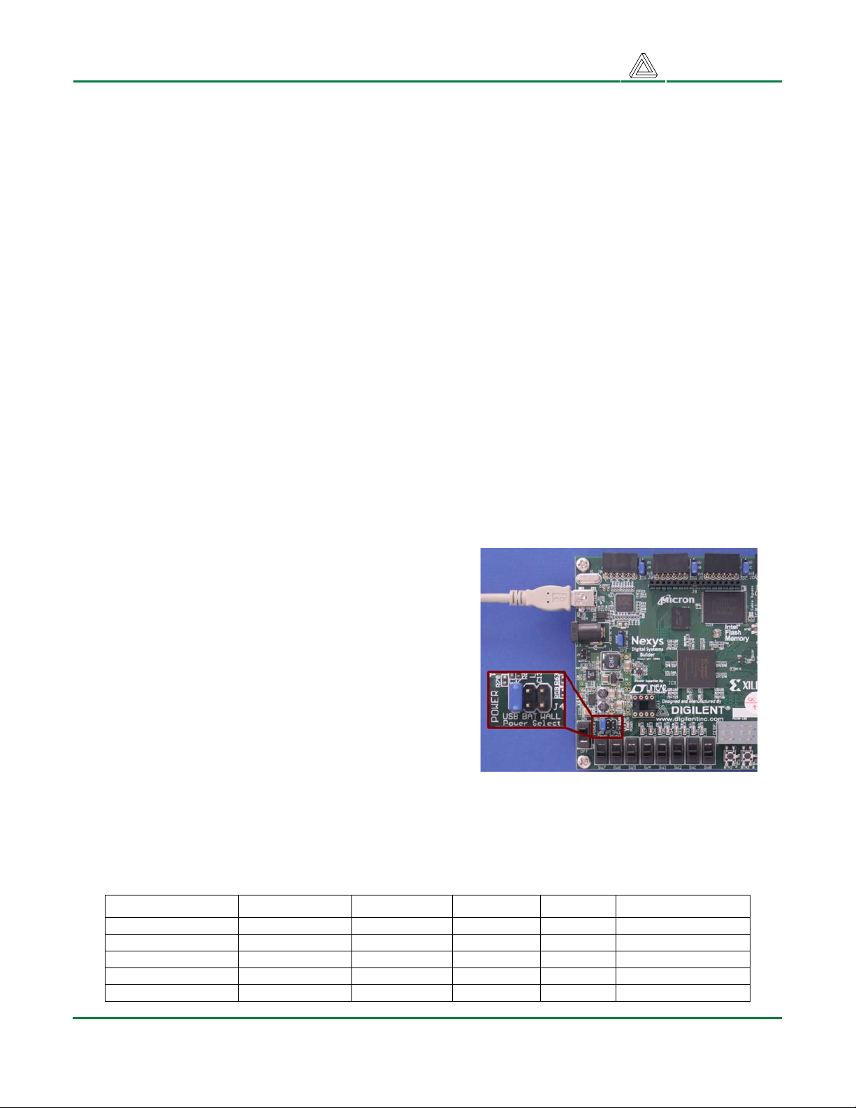
Power Supply
The Nexys board can be powered from the USB port or
any DC supply that produces a voltage in the 5VDC9VDC range. The power jack on the Nexys board
requires a center-positive, 2.1mm power supply
connector as is commonly found on wall-plug power
supplies. Voltages higher than 10V may permanently
damage Nexys.
The “raw” voltage from the power jack is routed to the
four 6-pin expansion connectors, the 16-pin expansion
connector, and to a 3.3V voltage regulator. The 2.5V
and 1.2V supplies required by the FPGA are generated
from the 3.3V supply. Total board current is dependant
on FPGA configuration, clock frequency, and external
connections. In test circuits with roughly 20K gates routed, a 50MHz clock source, and all LEDs
illuminated, about 200mA of current is drawn from the 1.2V supply, 50mA from the 2.5V supply, and
100mA from the 3.3V supply. Required current will increase if larger circuits are configured in the
FPGA, and if peripheral boards are attached. The table below summarizes the power supply
parameters.
Vendor
Linear Technology Switcher Main power 3.3V (IC6) LTC1765 3A/100mA
Linear Technology Switcher (dual) FPGA Vaux 2.5V (IC7) LTC3417 1.4A/50mA
Linear Technology Switcher (dual) FPGA Vcore 1.2V (IC7) LTC3417 1.4A/200mA
Linear Technology Linear Vsram 1.8V (IC8) LTC1844 150mA/90mA
Linear Technology Linear Vusb 3.3V (IC4) LTC1844 150mA/60mA
Technology Use Supply PN Current (Max/typ)
Copyright Digilent, Inc. Page 3/10 Doc: 502-107
Page 4

Nexys Reference Manual
Digilent
www.digilentinc.com
The Nexys board uses a six layer PCB, with the inner layers dedicated to VCC and GND planes. The
FPGA and the other ICs on the board all have a large complement of bypass capacitors placed as
close as possible to each VCC pin. The power supply routing and bypass capacitors result in a very
clean, low-noise power supply.
Oscillators
The Nexys board includes a primary, usersettable silicon oscillator that produces 25MHz,
50MHz, or 100MHz based on the position of the
clock select jumper at JP4. A socket for a second
oscillator is also provided at IC11 (the IC11
socket can accommodate any 3.3V CMOS
oscillator in a half-size DIP package). The primary
and secondary oscillators are connected to global
clock input pins at pin A8 and pin R9 respectively.
Both clock inputs can drive the clock synthesizer
DLL on the Spartan 3, allowing for a wide range
of internal frequencies, from 4 times the input
frequency to any integer divisor of the input
frequency.
Spartan-3E
FPGA
A8 CLK_OUT
R9
Linear Tech.
LTC6905
Oscillator
Oscillator
Socket
CLK_OUT
Frequency
Select
Jumper
25MHz
50MHz
100MHz
User I/O
The Nexys board includes several Input and Output devices, and several data ports so that many
designs can be implemented without the need for any other components.
Copyright Digilent, Inc. Page 4/10 Doc: 502-107
Page 5

Nexys Reference Manual
Digilent
www.digilentinc.com
Buttons
Slide
Switches
3.3V
BTN0
BTN1
BTN2
BTN3
3.3V
SW0
SW1
SW2
SW3
SW4
SW5
SW6
SW7
J13
K14
K13
K12
N15
J16
K16
K15
L15
M16
M15
N16
Spartan 3
FPGA
L14
L13
M14
L12
N14
M13
P14
R16
G14
G12
G13
F12
F13
E13
G15
H13
J14
E14
G16
H14
LD0
LD1
LD2
LD3
LD4
LD5
LD6
LD7
CA
CB
CC
CD
CE
CF
CG
DP
LEDs
3.3V
AN0
AN1
AN2
AN3
Inputs: Slide Switches and Pushbuttons
Four pushbuttons and eight slide switches are provided for circuit inputs. Pushbutton inputs are
normally low, and they are driven high only when the pushbutton is pressed. Slide switches generate
constant high or low inputs depending on their position. Pushbutton and slide switch inputs use a
series resistor for protection against short circuits (a short circuit would occur if an FPGA pin assigned
to a pushbutton or slide switch was inadvertently defined as an output).
Outputs: LEDs
Eight LEDs are provided for circuit outputs. LED anodes are driven from the FPGA via 390-ohm
resistors, so a logic ‘1’ output will illuminate them with 3-4ma of drive current. A ninth LED is provided
as a power-on LED, and a tenth LED indicates FPGA programming status.
Outputs: Seven-Segment Display
The Nexys board contains a four-digit common anode seven-segment LED display. Each of the four
digits is composed of seven segments arranged in a “figure 8” pattern, with an LED embedded in
each segment. Segment LEDs can be individually illuminated, so any one of 128 patterns can be
displayed on a digit by illuminating certain LED segments and leaving the others dark. Of these 128
possible patterns, the ten corresponding to the decimal digits are the most useful.
Copyright Digilent, Inc. Page 5/10 Doc: 502-107
Page 6

Nexys Reference Manual
Digilent
www.digilentinc.com
The anodes of the seven LEDs forming
each digit are tied together into one
Common anode
“common anode” circuit node, but the LED
cathodes remain separate. The common
anode signals are available as four “digit
AN0 AN1 AN2 AN3
F
A
B
enable” input signals to the 4-digit display.
The cathodes of similar segments on all four
displays are connected into seven circuit
nodes labeled CA through CG (so, for
example, the four “D” cathodes from the
four digits are grouped together into a single
circuit node called “CD”). These seven
cathode signals are available as inputs to
CA CB CCCD CE CF CG DP
E
Four-digit Seven
Segment Display
Individual cathodes
G
D
C
DP
the 4-digit display. This signal connection
scheme creates a multiplexed display, where the
cathode signals are common to all digits but they
can only illuminate the segments of the digit whose
corresponding anode signal is asserted.
A scanning display controller circuit can be used to
show a four-digit number on this display. This
circuit drives the anode signals and corresponding
cathode patterns of each digit in a repeating,
continuous succession, at an update rate that is
faster than the human eye can respond. Each digit
is illuminated just one-quarter of the time, but
because the eye cannot perceive the darkening of
a digit before it is illuminated again, the digit appears continuously illuminated. If the update or
“refresh” rate is slowed to a given point (around 45 hertz), then most people will begin to see the
display flicker.
In order for each of the four digits to
appear bright and continuously
Refresh period = 1ms to 16ms
illuminated, all four digits should be driven
once every 1 to 16ms (for a refresh
frequency of 1KHz to 60Hz). For example,
in a 60Hz refresh scheme, the entire
display would be refreshed once every
16ms, and each digit would be illuminated
for ¼ of the refresh cycle, or 4ms. The
controller must assure that the correct
cathode pattern is present when the
corresponding anode signal is driven. To
Cathodes
AN1
AN2
AN3
AN4
Digit 0
Digit period = Refresh / 4
Digit 1 Digit 2 Digit 3
illustrate the process, if AN0 is asserted
while CB and CC are asserted, then a “1” will be displayed in digit position 1. Then, if AN1 is asserted
while CA, CB and CC are asserted, then a “7” will be displayed in digit position 2. If AN0 and CB, CC
are driven for 4ms, and then A1 and CA, CB, CC are driven for 4ms in an endless succession, the
display will show “17” in the first two digits. An example timing diagram for a four-digit controller is
provided.
Ports and External Connectors
Copyright Digilent, Inc. Page 6/10 Doc: 502-107
Page 7

Nexys Reference Manual
USB Port
The Nexys contains an integral USB2
circuit based on a Cypress CY7C68013
USB controller. The USB port can be used
to program the on-board Xilinx devices, to
perform user-data transfers at up to
37Mbytes/sec, and to provide power to
the board. Programming is accomplished
with Digilent’s free Adept Suite Software.
The power source for the board is
determined by shorting the appropriate
pins at J4. Programming files are
generated with a number of software
packages (Digilent recommends the free
ISE WebPack from Xilinx). Once the
programming files are generated
programming the board is accomplished
via the Export function included in the
Adept Suite download.
The USB port on the Nexys board can
also accommodate data transfer with the
PC. The Adept Suite provides a software
interface to assist the user with this
function as well. The USB circuit on the
Nexys allows great flexibility when using
the board.
6-pin header connectors
The Nexys board provides four 6-pin
peripheral module connectors. Each
connector provides Vdd, GND, and four
unique FPGA signals. All four 6-pin
header circuits have short circuit
protection resistors and ESD protection
Diodes.
Several 6-pin module boards that can
attach to this connector are available
from Digilent, including speaker boards,
H-bridge boards, sensor boards, etc.
Please see www.digilentinc.com
more information.
16-pin header connectors
The Nexys board provides a 16-pin
header connector for use with several
for
Spartan 3
FPGA
GND
VDD
P16
P15
T7
R5
N15
J16
K16
K15
L15
M16
M15
N16
R6
R7
Digilent
www.digilentinc.com
1
2
16-pin
3
header
4
J8
5
6
7
8
9
10
11
12
13
14
15
16
Copyright Digilent, Inc. Page 7/10 Doc: 502-107
Page 8

Nexys Reference Manual
Digilent
www.digilentinc.com
16-pin interface modules that are currently in design or production. The 16-pin interface is designed
to provide for the use of a VGA module, a character LCD module and a Graphic LCD Module. The
connector provides Vdd, GND, and fourteen unique FPGA signals. The 16 pin header has short
circuit protection resistors.
Several 6-pin module boards that can attach to this connector are available from Digilent, including
speaker boards, H-bridge boards, sensor boards, etc. Please see www.digilentinc.com
for more
information.
Memory
The Nexys contains an Intel
JS28F320J3, 32 Mbit
StartaFlash and a Micron
MT45W8MW16 128Mbit
Cellular RAM. These two
devices share the OE, WE
and all ADDRESS and DATA
control signals.
FPGA Pin Assignment
Tables
Spartan 3
FPGA
IC13 only
See table
See table
K2
T3
B1
C2
J2
J1
K1
L2
C1
ADDR(23:0)
DATA(15:0)
OE
WE
MT-ADV
MT-CLK
MT-UB
MT-LB
MT-CF
MT-CRE
MT-WAIT
M45W8MW16
Cellular RAM
(8Mbyte x 16)
IC13
IC14
Micron
IC14 only
R4
T4
E4
BYTE
ST-STS
RP#
ST-CF
Intel
StrataFlash
JS28F320
(32 Mbit)
Copyright Digilent, Inc. Page 8/10 Doc: 502-107
Page 9

Nexys Reference Manual
A
Hirose FX2 Connector Pin Assignments
J1A Name FPGA J1B Name FPG
VCC3V3
1
2 VCC3V3 2 GND
3 TMS C13 3 TDO-ROM
4 JTSEL 4 TDK C14
5 TDO-FX2 5 GND
6 FX2-IO1 B4 6 GND
7 FX2-IO2 A4 7 GND
FX2-IO3
8
FX2-IO4
9
FX2-IO5
10
FX2-IO6
11
FX2-IO7
12
FX2-IO8
13
FX2-IO9
14
FX2-IO10
15
FX2-IO11
16
FX2-IO12
17
FX2-IO13
18
FX2-IO14
19
FX2-IO15
20
FX2-IO16
21
FX2-IO17
22
FX2-IO18
23
FX2-IO19
24
FX2-IO20
25
FX2-IO21
26
FX2-IO22
27
FX2-IO23
28
FX2-IO24
29
FX2-IO25
30
FX2-IO26
31
FX2-IO27
32
FX2-IO28
33
FX2-IO29
34
FX2-IO30
35
FX2-IO31
36
FX2-IO32
37
FX2-IO33
38
FX2-IO34
39
FX2-IO35
40
FX2-IO36
41
FX2-IO37
42
FX2-IO38
43
FX2-IO39
44
FX2-IO40
45
GND
46
FX2-CLKOUT
47
GND
48
VCCFX2
49
VCCFX2
50
1 SHIELD
C5 8
B5 9
E6 10
D6 11
C6 12
B6 13
E7 14
D7 15
C7 16
B7 17
D8 18
C8 19
A10 20
B10 21
D10 22
E10 23
B11 24
C11 25
D11 26
E11 27
B12 28
C12 29
A13 30
B13 31
A14 32
B14 33
B16 34
C16 35
C15 36
D14 37
D15 38
D16 39
E15 40
E16 41
F14 42
F15 43
H15 44
H16 45 GND
46 FX2-CLKIN C9
D9 47 GND
48 FX2-CLKIO B8
49 VCCFX2
50 SHIELD
GND
GND
GND
GND
GND
GND
GND
GND
GND
GND
GND
GND
GND
GND
GND
GND
GND
GND
GND
GND
GND
GND
GND
GND
GND
GND
GND
GND
GND
GND
GND
GND
GND
GND
GND
GND
GND
Digilent
www.digilentinc.com
Memory Pin
Assignments
ADDR Pin FPGA
Pin
ADR23 C3 DB15 D2
ADR22 A3 DB14 E2
ADR21 M4 DB13 D1
ADR20 D3 DB12 E1
ADR19 G5 DB11 F2
ADR18 H3 DB10 G2
ADR17 G4 DB9 G1
ADR16 L4 DB8 H1
ADR15 F3 DB7 R3
ADR14 M3 DB6 R1
ADR13 L5 DB5 P1
ADR12 N3 DB4 P2
ADR11 F5 DB3 N1
ADR10 F4 DB2 N2
ADR9 E3 DB1 M1
ADR8 G3 DB0 M2
ADR7 K4
ADR6 H4
ADR5 K3
ADR4 J4
ADR3 L3
ADR2 K5
ADR1 J3
DATA
Pin
FPGA
Pin
Copyright Digilent, Inc. Page 9/10 Doc: 502-107
Page 10

Nexys Reference Manual
Pin Name
1 JA-1 T14 1 JB-1 T12 1 JC-1 D5 1 JD-1 A9
2 JA-2 R13 2 JB-2 R11 2 JC-2 P9 2 JD-2 A12
3 JA-3 T13 3 JB-3 P8 3 JC-3 A5 3 JD-3 C10
4 JA-4 R12 4 JB-4 T10 4 JC-4 A7 4 JD-4 D12
5 GND 5 GND 5 GND 5 GND
6 VCC 6 VCC 6 VCC 6 VCC
FPGA
Pin
PMOD Expansion Connector Pin Assignments
Pin Name
FPGA
Pin
Pin Name
FPGA
Pin
Digilent
www.digilentinc.com
Pin Name FPGA
Pin
Copyright Digilent, Inc. Page 10/10 Doc: 502-107
 Loading...