

Page 1
1300 Henley Court
DOC#: 6015-502-001
Copyright Digilent, Inc. All rights reserved.
Other produc t and compa ny names mentioned may be trademarks of their res pective owne rs.
Page 1 of 21
Pullman, WA 99163
509.334.6306
www.digilentinc.com
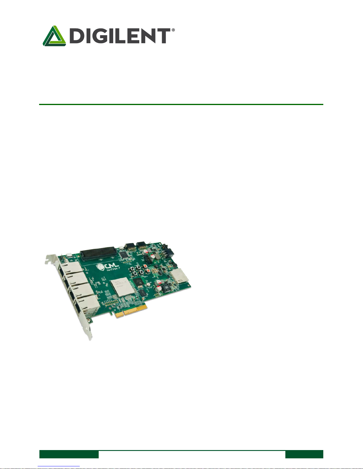
NetFPGA-1G-CML™ Board Reference Manual
Revised July 16, 2014
This manual applies to the NetFPGA-1G-CML rev. E
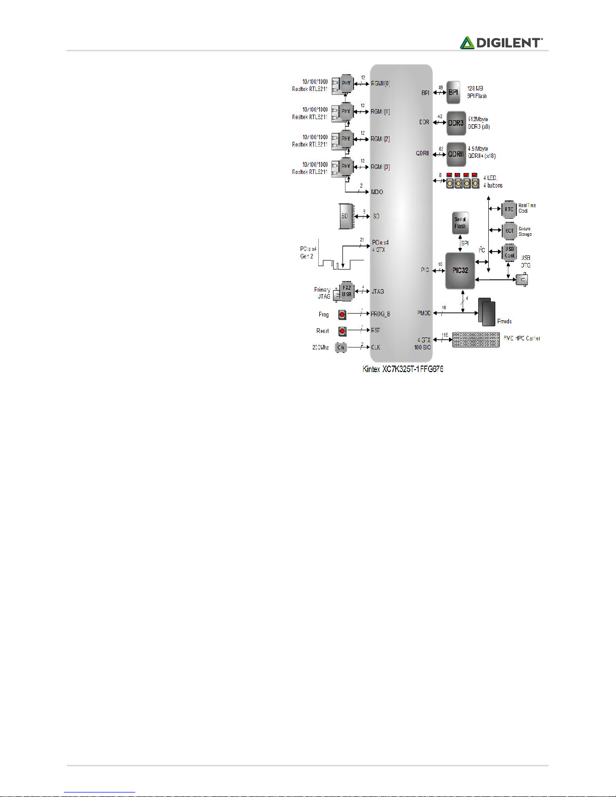
Overview
The NetFPGA-1G-CML is a versatile, low-cost network hardware development platform featuring a Xilinx® Kintex®7 XC7K325T FPGA and includes four Ethernet interfaces capable of negotiating up to 1 GB/s connections. 512 MB
of 800 MHz DDR3 can support high-throughput packet buffering while 4.5 MB of QDRII+ can maintain low-latency
access to high demand data, like routing tables. Rapid boot configuration is supported by a 128 MB BPI Flash,
which is also available for non-volatile storage applications. The standard PCIe form factor supports high speed x4
Gen 2 interfacing. The FMC carrier connector provides a convenient expansion interface for extending card
functionality via Select I/O and GTX serial interfaces. The FMC connector can support SATA-II data rates for
network storage applications. The FMC connector can also be used to extend functionality via a wide variety of
other cards designed for communication, measurement, and control.
• Xilinx Kintex-7 XC7K325T-1FFG676 FPGA
• Low-jitter 200 MHz oscillator
• Four 10/100/1000 Ethernet PHYs with
RGMII
• X4 Gen 2 PCI Express
• X16 4.5 MB QDRII+ static RAM (450 MHz)
• X8 512 MB DDR3 dynamic RAM (800 MHz)
• 1-Gbit BPI Flash
• SD card slot
• 32-bit PIC microcontroller
• USB microcontroller
• Real time clock
• Crypto-authentication chip
• High pin count FMC connector (VITA 57)
withh 100 Select-IO and 4 GTX serial pairs
• Two Pmod connectors
The NetFPGA-1G-CML board.
The NetFPGA-1G-CML is designed to support the Stanford NetFPGA architecture with reference designs available
through the NetFPGA GitHub Organization (www.github.com/organizations/NetFPGA). It is fully compatible with
Xilinx Vivado™ and ISE® Design Suites as well as Xilinx SDK for embedded software design.
• Four on-board LEDs and four on-board
general-purpose buttons
Page 2
NetFPGA-1G-CML™ Board Reference Manual
Copyright Digilent, Inc. All rights reserved.
Other produc t and compa ny names mentioned may be trademarks of their res pective owne rs.
Page 2 of 21
The Kintex-7 XC7K325T-1FFG676 FPGA has ample
logic and I/O capacity for supporting a wide range
of designs with the following capabilities:
• 50,950 slices, each containing four 6-
input LUTs and eight flip-flops
• Over 16 Mbit of fast on-chip block RAM
• Ten clock management tiles with one PLL
and one mixed-mode clock manager each
• 840 DSP slices
• Integrated PCI Express
• Integrated AES bitstream encryption and
SHA-256 authentication with batterybacked encryption key
• 400 Select I/O ports (250 high range, 150
high speed)
• Eight 6.6 Gb/s GTX serial transceivers
1 FPGA Configuration
The system logic configuration is stored within the FPGA in SRAM-based memory cells. This data defines the
FPGA's logic functions and circuit connections, but it is volatile since it remains valid only as long as power is
applied. Because of this, the device is configured (i.e., programmed) every time it is turned-on. In addition, it may
also be re-configured at any time power is applied. Once power is removed, the most recently programmed logic
configuration is lost. The configuration data is commonly called a bitstream which is most often contained in files
of type ".bit" or ".mcs". These files may be created several different ways using Xilinx development software.
The FPGA may be configured from three different sources. These include the on-board BPI flash, an off-board USB
flash drive, or via a PC. The NetFPGA-1G follows a specific configuration sequence when it powers up and comes
out of reset. If a valid "download.bit" file is detected on an attached UBS flash drive, that bitstream will be used to
program the FPGA. The flash drive must be FAT formatted, contain a single "download.bit" file, and be attached to
the USB-HOST port (J13) with jumper JP4 in place. If no flash drive bitstream is detected, an attempt will be made
to configure the device from the on-board BPI flash address 0x0. If no flash bitstream is available, the board idles
until it is programmed from a PC. PC programming can be done either via a USB cable connected to the USB PROG
port (J12), or a JTAG programming cable connected to the Xilinx PROG CABLE port (J15). Any flash drive bitstreams
that are not built for the Xilinx XC7K325T FPGA will be ignored. This power-on programming sequence can be reinitiated at any time after power is applied by depressing the red PROG button (BTN5).
Both Digilent and Xilinx distribute free software that can be used to transfer bitstreams from a PC as well as create
bitstream files to load via a flash drive. Digilent's Adept and Xilinx's iMPACT applications can directly program the
FPGA using a .bit file a standard USB A to Micro B cable connected to J12 or through any of several Digilent JTAG
programming cables connected to J15. The on-board BPI flash is programmed via similar means. When
Page 3
NetFPGA-1G-CML™ Board Reference Manual
Copyright Digilent, Inc. All rights reserved.
Other produc t and compa ny names mentioned may be trademarks of their res pective owne rs.
Page 3 of 21
programming the BPI, iMPACT transfers a .mcs format bitstream to the flash in a two-step process. iMPACT first
programs the FPGA directly with a special purpose BPI flash interface. It will then transfer the .mcs bitstream to the
flash through that interface. This process is fully automated by the iMPACT program, so a designer only needs to
be concerned with the creation of the .mcs file using Xilinx's design software.
More details on configuring the XC7K325T FPGA via the on-board BPI (using Master BPI mode), via the PIC USBHOST (using Slave Serialmode), and via the JTAG mode can be found in the Xilinx 7 Series FPGAs Configuration User
Guide (UG470).
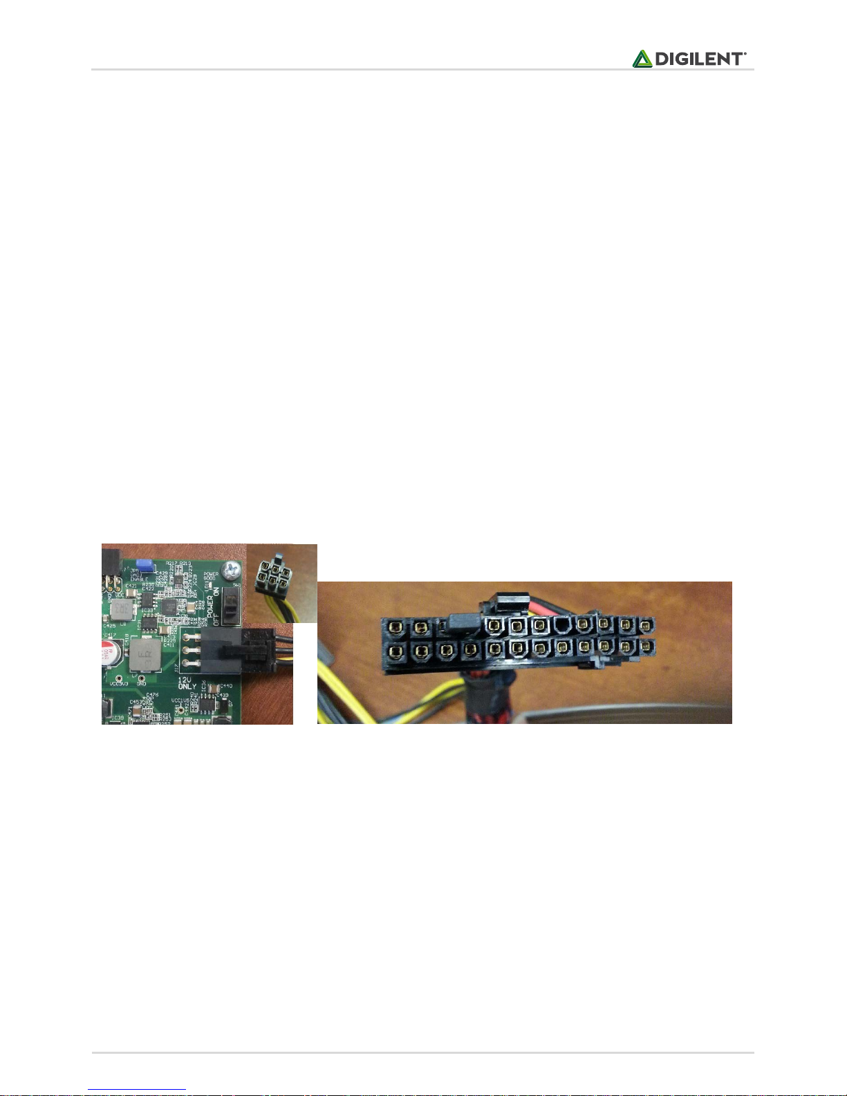
2 Power Supplies
The NetFPGA-1G requires a 12V, 5A, or greater power source. Power is supplied via the J17 Molex connector at the
rear of the PCB, as is often done with high performance PC graphics cards. No power is supplied via the PCIe
motherboard bus connector.
The NetFPGA-1G can be powered using the 6-pin PCIe power supply connector (Fig. 1) of any standard ATX power
supply. When installed on a PC motherboard, you can directly plug the 6-pin PCIe power supply connector of your
PC power supply into J17. When used standalone (without a motherboard), you need to short pins 15 and 16
(pulling down PS_ON signal) of the main 20-pin connector of the standard ATX power supply to power-on the ATX
unit (Fig.1).
Figure1. Left: NetFPGA-1G can be powered by plugging the 6-pin PCIe power connector in J17; Right: Pin 16 and 17 are shorted using a jumper
to power on a standard ATX power supply when used standalone.
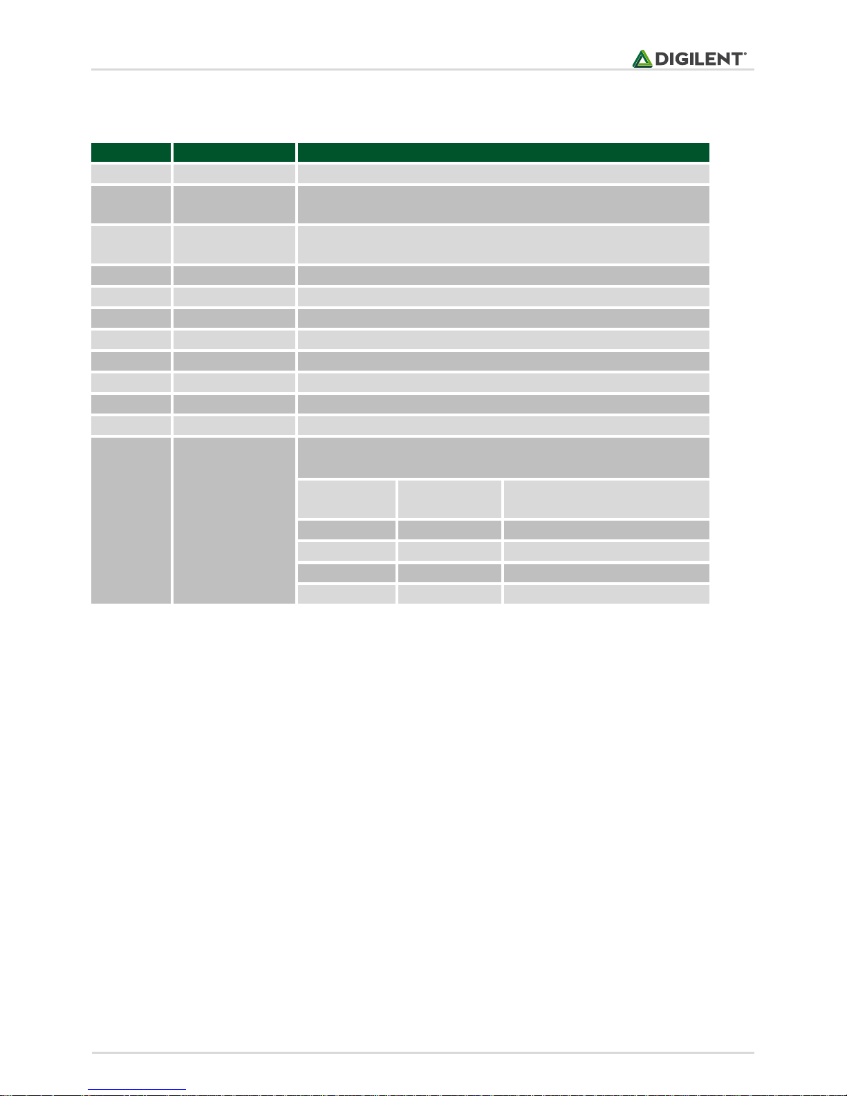
Analog Devices voltage regulators provide a number of on-board power and reference voltages that are derived
from the main 12V supply, as shown in Table 1. Supply power-on and power-off sequencing follows manufacturer
recommendations. The on-board battery that supports encryption key storage and the real-time clock is charged
when the PCB is powered on and should not need to be replaced during the lifetime of the board.
VADJ controls the signal levels used between the FMC connector and two FPGA Select I/O banks and can be set to
1.2 V, 1.8 V, 2.5 V, or 3.3 V as needed. The board is shipped with the VADJ supply turned off. To turn on VADJ,
jumper JP5 is installed and the FPGA is configured to drive the VADJ_EN pin (AD16) high. The VADJ voltage is
selected via the FPGA configuration using pins AF19 and AF20 as shown in Table 1.
When jumper JP4 is in place, the USB HID connector provides 5V at up to 0.5 A to external USB devices, including
keyboards, mice, and thumb drives. An Analog Devices ADM1177 hot swap controller and power monitor is used
to allow safe device attachment and removal while the board is powered up. The PIC can also measure USB
current and voltage by accessing the on-chip power monitor via the PIC I2C peripheral bus.
Page 4
NetFPGA-1G-CML™ Board Reference Manual
Copyright Digilent, Inc. All rights reserved.
Other produc t and compa ny names mentioned may be trademarks of their res pective owne rs.
Page 4 of 21
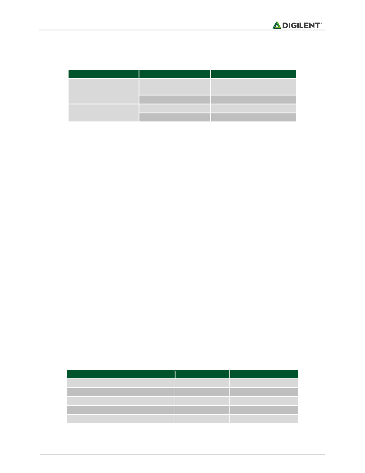
Supply
Derived From
Application
5.0 V
12.0 V
USB HID; FMC
SD Card; Ethernet PHYs; Cypress FX2LP; Microchip PIC; BPI
FPGA auxiliary supply, VCC
; Backup battery; Real-time clock
1.8 V
12.0 V
QDRII+ supply
1.8 V
3.3 V
FPGA GTX transceiver Quad PLL
1.5 V
12.0 V
DDR3; FPGA I/O Bank 34
1.2 V
12.0 V
FPGA GTX transceiver termination
1.0 V
12.0 V
FPGA GTX analog supply
1.0 V
3.3 V
FPGA Core
0.9 V
3.3 V
QDRII+ reference
0.75 V
3.3 V
DDR3 reference
SET_VADJ2
SET_VADJ1
0
0
1.2 V
0
1
1.8 V
1
0
2.5 V
1
1
3.3 V
The Xilinx Kintex-7 Data Sheet: DC and AC Switching Characteristics (DS182) provides more information on the
power supply requirements of the FPGA board.
3.3 V 12.0 V
2.0 V 5.0 V
VADJ 12.0 V
Flash; FPGA I/O Banks 14,15; FMC; PMODs
BAT
backup.
FPGA I/O Banks 12, 13; FMC; Configurable.
FPGA AF20
FPGA AF19
VADJ
Table 1. On-board power supplies.
3 Oscillators and Clocks
On-board oscillators support various board subsystems. A low-jitter 125 MHz oscillator is provided for the Ethernet
PHYs and a 50 MHz oscillator drives the FPGA master configuration clock. The Cypress FX2LF and Microchip PIC
microcontroller each contain on-chip oscillators running at 24 MHz and 8 MHz, respectively.
The main FPGA system clock is provided by an ultra-low-jitter 200 MHz differential oscillator connected to pins
AA2 and AA3 in I/O bank 34. This can drive up to ten internal PLLs (Phase Locked Loops) and MMCMs (MixedMode Clock Managers) on the FPGA for high-performance multi-clock-domain designs. Please refer to the Xilinx 7-
Series Clock Resources User Guide (UG472) for more details on FPGA internal clocking resources.
4 FPGA Memory
The XC7K325T FPGA includes 445 on-chip Block RAMs (BRAMs) of 36Kb, or 4096 bytes with two-bit error
correction, which amounts to a total of 1.78 MB of on-chip, error-corrected static RAM that can be used for a
variety of purposes ranging from program storage for deeply embedded "bare metal" applications to data
Page 5

NetFPGA-1G-CML™ Board Reference Manual
Copyright Digilent, Inc. All rights reserved.
Other produc t and compa ny names mentioned may be trademarks of their res pective owne rs.
Page 5 of 21
buffering and table lookup. Each 36Kb BRAM can be partitioned into two completely independent 18Kb RAMs to
help facilitate more efficient hardware utilization. Furthermore, each BRAM can be configured for dual-port
operation and includes register infrastructure tp support FIFO functionality. These BRAM ports can be organized in
either single or dual-clock configurations. The Xilinx tool chain includes a rich selection of resources for on-chip
BRAM configuration and initialization. Further information is provided in the Xilinx 7-Series FPGAs Memory
Resources User Guide (UG473).
5 DDR3 Memory
The NetFPGA-1G includes a Micron MT41K512M8 512 MB DDR3 SDRAM which employs an 800 MHz byte-wide
data bus capable of operating at a data rate of 1600 MT/s. Project development with the SDRAM involves using
the Xilinx Memory Interface Generator (MIG) in either the XPS design tool or the Vivado Design Suite. The MIG is
an interface generation wizard for selecting part types and configuring FPGA Select I/O resources for the memory
hardware interface. The interface is automatically configured by the MIG for use with the AXI4 system bus and
provides options for 2:1 or 4:1 memory-to-bus clock ratios. The NetFPGA-1G uses a VCC
high performance DDR3 frequency settings. Please see the Xilinx 7 Series FPGAs Memory Interface Solutions User
Guide (UG586) and the Micron 4Gb:x4,x8,x16 DDR3L SDRAM data sheet for more details.
AUX-IO of 2.0V to support
6 QDRII+ Memory
A 4.5 MB Cypress CY7C2263KV18 QDRII+ Quad Data Rate SRAM is provided for applications that require high
speed, low-latency memory. Common applications include FIFO buffers and table lookups. The notion of "Quad"
data rate comes from the ability to simultaneously read from a unidirectional read port and write to a
unidirectional write port on both clock edges. The NetFPGA-1G QDRII+ is capable of operating at up to 450MHz to
yield data transfer rates of up to 900 MT/s per 2-byte port. This yields a peak bandwidth of up to 3.6 GB/s. The
Xilinx Memory Interface Generator (MIG) is able to generate and configure an AXI4 based interface into the QDRII+
via the user friendly wizard tool. More information regarding the QDRII+ memory part and the Xilinx MIG tool can
be found in the Cypress CY7C2263KV18/CY7C2265KV18 data sheet, the Cypress Application Note QDR-II, QDR-II+,
DDR-II, DDR-II+ Design Guide (AN4065), and the Xilinx 7 Series FPGAs Memory Interface Solutions User Guide
(UG586).
7 BPI Flash Memory
A 1-Gbit Numonyx BPI (Byte Peripheral Interface) flash memory in a 128 MB x16 configuration is provided to
support high-speed FPGA configuration after board reset. High-speed single-step configuration enables
enumeration via the PCIe interface within 100 mS, as required by the PCI specification. In BPI configuration mode,
the FPGA acts as the bus master, driving the flash address and control signals to transfer previously stored
bitstream data into the configuration SRAM.
The BPI flash has enough capacity to store multiple device configurations. This facilitates multi-stage configuration
boot as well as applications that utilize dynamic reconfiguration. Configuration bitstreams are not the only data
which can be stored in the BPI flash. After configuration is complete, the BPI programming pins may be used as
normal Select I/O within the design. As a result, non-volatile data of any type can also be stored to and retrieved
from the BPI after device configuration is complete. More information regarding BPI based device configuration is
Page 6

NetFPGA-1G-CML™ Board Reference Manual
Copyright Digilent, Inc. All rights reserved.
Other produc t and compa ny names mentioned may be trademarks of their res pective owne rs.
Page 6 of 21
available in the Xilinx 7-Series FPGAs Configuration User Guide (UG470) and application note XAPP587 BPI Fast
Flash Memory data sheet for more specifics regarding device operation.
8 SD Card
The NetFPGA-1G SD card connector supports a second non-volatile storage resource which is also removable. This
connector supports a standard size SD memory card and meets all physical layer requirements of both SPI and SD
bus protocols. It supports the UHS-I pin assignment standard (but not UHS-II) and provides high speed signaling at
3.3V to support SC, HC, and XC class SD cards. Please see SD Specifications Part 1 Physical Layer Simplified
Specification by the Technical Committee of the SD Card Association for more details regarding the use of SD
memory cards with this connector.
9 PCIe Interface
The NetFPGA-1G is designed with a PCI-Express form factor to support interconnection with common processor
motherboards. Four of the FPGA's eight high speed serial GTX transceivers are dedicated to implementing up to
four-lanes of Gen. 2.0 (5 GB/s) PCIe communications with a host processing system. These transceivers work in
conjunction with the on-chip 7 Series Integrated PCI Express Block and synthesizable on-chip logic to provide a
scalable, high performance PCI Express I/O core.
This core is configured and incorporated into designs using either the Xilinx ISE Coregen tool or via instantiation
and customization from the Vivado Design Suite IP catalog. Please refer to the Xilinx 7 Series FPGAs Integrated
Block for PCI Express V2.0 (PG054) product guide and 7 Series FPGAs GTX/GTH Transceivers (UG476) user guide for
more information.
10 Ethernet PHYs
Four Realtek RTL8211 Ethernet transceivers (PHYs) are provided to interface to network connections via on-board
RJ-45 connectors. Each RJ-45 has two LEDs to indicate link status and activity. Each PHY controls three LEDs: two
on an associated RJ-45 and a third on-board (LD5-LD8). The Phys are programmed via a shared MDIO bus and are
accessed via MDIO addresses 1 through 4: corresponding to connectors ETH1 through ETH4 on the PCB. At reset,
each PHY defaults to 1Gbps with the LED configuration shown in Table 2.
On each RJ45, the bottom LED is the one that is closest to the PCIe connector. The default behavior of the onboard LED is to mimic that of the top RJ45 LED. The default auto-negotiation behavior allows each PHY to
independently adjust its rate to 10/100 Mbps or 1Gbps as needed.
Data is transferred to and from the PHYs via a Reduced Gigabit Media Independent Interface (RGMII). This is
similar to the Gigabit Media Independent Interface (GMII), which uses eight bits for both transmit and receive
data. RGMII achieves the same data rate with half the number of data bits and double-data-rate clocking. 1 Gbps
data transfers are thereby achieved using a 125MHz clock with four bits transferred on each clock edge for both
send and receive. This provides a significant reduction in the number of FPGA I/O pins required to support the four
Ethernet interfaces.
Page 7
NetFPGA-1G-CML™ Board Reference Manual
Copyright Digilent, Inc. All rights reserved.
Other produc t and compa ny names mentioned may be trademarks of their res pective owne rs.
Page 7 of 21
LED
Action
Meaning
Connection Negotiation
On
Link activity present
Off
No link activity
Fast blink
Link activity present
Component Name
PIC I2C Controller
I2C 7-bit Address
AD5274 Digital Rheostat
I2C2
0101110
ADM1177 Hot Swap Controller
I2C2
1011011
ATSHA204 CryptoAuthentication
I2C2
1100100
M41T62 Real-Time Clock
I2C2
1101000
24LC128 Serial EEPROM
I2C1
1010001
Xilinx provides Ethernet MAC IP that will support 10/100/1000 Mb/s via the ISE Design Suite Coregen tool and the
Vivado design suite. Please refer to Xilinx Product Guide PG051 LogiCORE IP Tri-Mode Ethernet MAC for more
information.
RJ45 Top
Slow blink
Complete
RJ45 Bottom
Table 2. RJ-45 Ethernet Connector LED Function.
11 PIC Subsystem
NetFPGA-1G includes a 32-bit PIC microcontroller for managing USB OTG, real-time clock, and secure storage
interfacing. The PIC is pre-programmed with manufacturing test code and an ability to load FPGA bitstreams from
a USB memory stick. It is possible to re-program the PIC to support end-user applications that make use of various
other PIC subsystem features. This may be done via J14 using a PICKit 3 In-Circuit Debugger (Digilent p/n
PG164130).
To run the pre-programmed manufacturing test, first set up the NetFPGA-1G and host PC as described in Appendix
A: Manufacturing Test. When the board is powered on, the factory-loaded PIC firmware will search for the
bitstream "mfg_test.bit" on the USB flash drive and use it to configure the FPGA in slave serial mode. After the
FPGA has been configured, a test menu will be displayed on the terminal emulator window connected to the
PmodUSBUART, and the user can run the tests by following the menu prompts. If the board is set up as described
in Appendix A, all tests should pass.
The address map of the PIC I
Serial Flash using general-purpose I/O ports for increased data storage. The flash's pins are connected to the PIC
ports as shown in Table 4.
To program the PIC device, connect a PICkit 3 to the NetFPGA-1G by placing a 1x6 pin header in the zig-zag
connector J14 and connect it to the PICkit 3 using a 6-pin cable. If Digilent's 6-pin Pmod cable is used, the white
indicator dot on the NetFPGA-1G side should be above pin 6, and the dot on the PICkit 3 side will be face-up and
opposite the white arrow on the PICkit 3. The PIC can then be programmed from Microchip's MPLAB X or MPLAB
IPE by selecting the PICkit 3 as the programming tool.
2C peripherals is shown in Table 3. The PIC is also connected to an MX25L12835E SPI
2
Table 3. PIC I
C peripheral address map.
Page 8

NetFPGA-1G-CML™ Board Reference Manual
Copyright Digilent, Inc. All rights reserved.
Other produc t and compa ny names mentioned may be trademarks of their res pective owne rs.
Page 8 of 21
Flash Pin
PIC Port
CS
RB10
SCLK
RB11
SI
RB12
SO
RB13
WP
RB14
HOLD
RB15
Table 4. PCI Flash connections.
12 On-Board I/O
Built-in on-board I/O includes four LEDs and six buttons. Four of the buttons are general-purpose and two are set
aside for special functions. The red special function buttons are reserved for use as an on-chip reset (BTN4 - RESET)
to reset the design logic and a configuration reset (BTN5 – PROG) which initiates a new FPGA configuration
sequence like that which occurs at power-on. It is important to note that the buttons and LEDs are not all
constrained to the same IOSTANDARD on their associated ports, since they are connected to otherwise unallocated ports in different FPGA IO banks. Please refer to Appendix B for specific details regarding the button and
LED IO port constraints.
13 Pmod Expansion Connectors
The NetFPGA-1G has two 12-pin connectors to support I/O expansion via Digilent Pmods. Digilent manufactures
Pmod accessories that support a large variety of external interfaces that increase system flexibility. The Pmod
connectors are 2x6 right-angle 100-mil female connectors that work with the standard 2x6 headers available from
a variety of distributors. On the NetFPGA-1G, each 12-pin Pmod connector provides two 3.3V VCC supply
connections (pins 6 and 12), two Ground connections (pins 5 and 11), and eight logic signals (Fig. 2). The supply
pins can provide up to 1A of current to connected Pmod devices. The logic signals are not matched pairs. They are
routed without impedance control or delay matching. Note also that the connectors are not keyed, so care should
be taken to verify that any connected devices have Pin 1 aligned with Pin 1 on the connector. Pin 1, VCC, and GND
are clearly labeled on the PCB to help simplify proper connection.
Figure 2. Pmod connectors, end view.
Page 9

NetFPGA-1G-CML™ Board Reference Manual
Copyright Digilent, Inc. All rights reserved.
Other produc t and compa ny names mentioned may be trademarks of their res pective owne rs.
Page 9 of 21
14 Expansion Connector
The NetFPGA-1G includes a VITA-57 compatible FMC (FPGA Mezzanine Card) carrier connector. A High Pin Count
(HPC) connector is used to provide the maximum possible compatibility with a variety of commercially available
mezzanine cards. Select I/O ports on the XC7K325T are connected to all of the standard Low Pin Count (LPC)
signals on the connector, but only 22 of the HPC signals are supported due to the limitations of the FF676 package.
Up to four differential send/receive pairs for GTX transceivers are also supported.
The FMC interface signals are driven by two Select I/O banks within the FPGA. Signal drive voltages within these
banks are configured together to match the various requirements of different mezzanine cards. These banks are
disabled on the board when shipped, but jumper JP5 (VADJ ENABLE) can be installed to prepare these I/O banks
for use with the FMC connector. Three control outputs are then included in the FPGA design configuration to set
the FMC signaling voltage and enable it. Those signals are VADJ_EN, SET_VADJ1, SET VADJ2, and are set according
to Table 1. Keep in mind that the IOSTANDARD required by the pin constraints associated with the FMC interface
will depend upon the VADJ selected, and that these VADJ programming signals should be set to constants within
the design.
Please refer to the American National Standards Institute ANSI/VITA 57.1 FPGA Mezzanine Card (FMC) Standard for
additional detail regarding standard FMC module and carrier requirements. Refer to Appendix B for specific I/O
constraints relating FPGA pins to their associated FMC control and connector pins.
Page 10

NetFPGA-1G-CML™ Board Reference Manual
Copyright Digilent, Inc. All rights reserved.
Other produc t and compa ny names mentioned may be trademarks of their res pective owne rs.
Page 10 of 21
Appendix A: Manufacturing Test
The following hardware is required to run all NetFPGA-1G Manufacturing tests:
• 1x HiTechGlobal PCI Express Test/SMA Breakout Board
• 8x SMA to SMA cable, 24"
• 2x Ethernet cables
• 1x NetFGPA-7 FMC Test Card
• 1x SD card, any size, loaded with an ASCII text file named "message.txt"
• 1x Micro (male) to Type A (female) USB adapter
• 1x USB thumb drive loaded with the production test bitstream, "mfg_test.bit"
• 1x PmodUSBUART
• 2x 6 pin connector cable, 6"
• 1x Micro (male) to Type A (male) USB cable
• 2x 1x6 pin headers
• 46x 2 pin block jumpers
• 12 V power supply
If debug information in addition to pass/fail messages regarding manufacturing tests related to the FPGA is
desired, an additional PmodUSBUART, 6 pin connector cable, and micro (male) to type A (male) USB cable is
needed.
The following summary describes how to set up the manufacturing test hardware with the NetFPGA-1G:
a) Load jumpers JP4 (USB HOST) and JP5 (VADJ ENABLE)
b) For both Pmod headers JA and JB, plug a 1x6 pin header in the bottom row (pins 7-12) and place a jumper
across pins 7-8 and another across pins 9-10
c) Connect the NetFPGA-7 FMC Test Card to the FMC connector J11 and load all the jumper blocks
horizontally (1 <-> 2, 3 <-> 4, 5 <-> 6, etc.)
d) Connect one Ethernet cable between ETH1 and ETH2, and another between ETH3 and ETH4
e) Connect the USB thumb drive containing "nf7_test.bit" to J13 using the micro to type A adapter cable
f) Plug the SD card containing "message.txt" into the SD connector J10
g) Connect a PmodUSBUART to pins 1-6 of JA using a 6 pin connector cable, and connect the PmodUSBUART
to a host machine using a micro to type A USB cable
h) Plug the NetFPGA-7 into the HTG PCIe test card. Loop the RX0-3 pairs on the HTG card to the TX0-4 pairs
using SMA cables (RX0P <-> TX0P, RX0N <-> TX0N, etc.). Set switches 1-3 on the HTG card to 000.
Additionally, power the HTG card with a Molex connector from a standard PC power supply, and ensure
the power switch is set to ATX
i) Plug a PCIe power connector from a standard PC power supply into J17 on the NetFPGA-7
j) If FPGA debug information is desired, connect the additional PmodUSBUART, 6 pin connector cable, and
micro (male) to type A (male) USB cable to pins 1-6 of Pmod connector JB and a host machine
Many tests can be run independently without the need for additional hardware. For example, the HiTech Global
Breakout Board is only needed to test the PCIe edge connector. More details regarding individual tests are
provided in the NetFPGA-1G Manufacturing Test Reference Manual available on the Digilent web site.
Page 11

NetFPGA-1G-CML™ Board Reference Manual
Copyright Digilent, Inc. All rights reserved.
Other produc t and compa ny names mentioned may be trademarks of their res pective owne rs.
Page 11 of 21
Port Name
IO Location
IO Standard Type
IOSTANDARD=LVCMOS18; # RESET
button (BTN4)
NET system_clk_p
LOC = AA3
IOSTANDARD=LVDS;
NET system_clk_n
LOC = AA2
IOSTANDARD=LVDS;
NET ddr3_dq[1]
LOC = AE3
IOSTANDARD = SSTL15_T_DCI;
NET ddr3_dq[3]
LOC = AF3
IOSTANDARD = SSTL15_T_DCI;
NET ddr3_dq[5]
LOC = AF2
IOSTANDARD = SSTL15_T_DCI;
NET ddr3_dq[7]
LOC = AE2
IOSTANDARD = SSTL15_T_DCI;
NET ddr3_addr[1]
LOC = Y2
IOSTANDARD = SSTL15;
NET ddr3_addr[2]
LOC = W3
IOSTANDARD = SSTL15;
Appendix B: FPGA Pin Constraints
The following list provides LOC and IOSTANDARD constraints for the main peripheral pins connected to the FPGA.
This information can be used in a design UCF file with Xilinx ISE Design Suite, a design XDC file with Xilinx Vivado
Design Suite, or with various interface generators included with Xilinx Coregen and MIG. Please see the Xilinx
Constraints Guide (UG625) for ISE Design Suite based designs and Xilinx Vivado Design Suite User Guide: Using
Constraints (UG903) for Vivado based designs.
Depending upon the design suite selected, this information can be expressed in either a UCF file or an XDC file as
follows:
UCF format used with ISE Design Suite
NET <port name> LOC=<io location> | IOSTANDARD=<io standard type>;
XDC format used with Vivado Design Suite
set_property IOSTANDARD <io standard type> [get_ports { <port list> }]
set_property LOC <io location> [get_ports <port name>]
The information is presented in UCF format to express a clear association between the pin and the desired IO
standard for the NetFPGA-1G, although it can be readily translated into the XDC format. LOC information is
provided here for all pins. IOSTANDARD information is provided for SelectIO pins. Other useful properties are
suggested where appropriate.
System Clock and Reset
NET reset LOC = AA8
DDR3 SDRAM
Port Name IO Location IO Standard Type
NET ddr3_dq[0] LOC = AE5 IOSTANDARD = SSTL15_T_DCI;
NET ddr3_dq[2] LOC = AD4 IOSTANDARD = SSTL15_T_DCI;
NET ddr3_dq[4] LOC = AE1 IOSTANDARD = SSTL15_T_DCI;
NET ddr3_dq[6] LOC = AD1 IOSTANDARD = SSTL15_T_DCI;
NET ddr3_addr[0] LOC = Y3 IOSTANDARD = SSTL15;
Page 12

NetFPGA-1G-CML™ Board Reference Manual
Copyright Digilent, Inc. All rights reserved.
Other produc t and compa ny names mentioned may be trademarks of their res pective owne rs.
Page 12 of 21
NET ddr3_addr[4]
LOC = AB2
IOSTANDARD = SSTL15;
NET ddr3_addr[5]
LOC = W1
IOSTANDARD = SSTL15;
NET ddr3_addr[6]
LOC = AC2
IOSTANDARD = SSTL15;
NET ddr3_addr[7]
LOC = U2
IOSTANDARD = SSTL15;
NET ddr3_addr[11]
LOC = Y1
IOSTANDARD = SSTL15;
NET ddr3_addr[12]
LOC = AC3
IOSTANDARD = SSTL15;
NET ddr3_addr[13]
LOC = V2
IOSTANDARD = SSTL15;
NET ddr3_addr[14]
LOC = AC1
IOSTANDARD = SSTL15;
NET ddr3_ba[1]
LOC = AC4
IOSTANDARD = SSTL15;
NET ddr3_ba[2]
LOC = V4
IOSTANDARD = SSTL15;
NET ddr3_ras_n
LOC = Y6
IOSTANDARD = SSTL15;
NET ddr3_cas_n
LOC = Y5
IOSTANDARD = SSTL15;
NET ddr3_odt[0]
LOC = U7
IOSTANDARD = SSTL15;
NET ddr3_cs_n[0]
LOC = U6
IOSTANDARD = SSTL15;
NET ddr3_dm[0]
LOC = AE6
IOSTANDARD = SSTL15;
NET ddr3_dqs_p[0]
LOC = AF5
IOSTANDARD = DIFF_SSTL15_T_DCI;
Port Name
IO Location
IO Standard Type
NET qdriip_d[0]
LOC = V8
IOSTANDARD = HSTL_I;
NET qdriip_d[1]
LOC = V7
IOSTANDARD = HSTL_I;
NET qdriip_d[2]
LOC = W9
IOSTANDARD = HSTL_I;
NET ddr3_addr[3] LOC = W5 IOSTANDARD = SSTL15;
NET ddr3_addr[8] LOC = AB1 IOSTANDARD = SSTL15;
NET ddr3_addr[9] LOC = V1 IOSTANDARD = SSTL15;
NET ddr3_addr[10] LOC = AD6 IOSTANDARD = SSTL15;
NET ddr3_addr[15] LOC = AD5 IOSTANDARD = SSTL15;
NET ddr3_ba[0] LOC = AA5 IOSTANDARD = SSTL15;
NET ddr3_we_n LOC = U5 IOSTANDARD = SSTL15;
NET ddr3_reset_n LOC = U1 IOSTANDARD = LVCMOS15;
NET ddr3_cke[0] LOC = AB5 IOSTANDARD = SSTL15;
NET ddr3_dqs_n[0] LOC = AF4 IOSTANDARD = DIFF_SSTL15_T_DCI;
NET ddr3_ck_p[0] LOC = AA4 IOSTANDARD = DIFF_SSTL15;
NET ddr3_ck_n[0] LOC = AB4 IOSTANDARD = DIFF_SSTL15;
QDRII+
Page 13

NetFPGA-1G-CML™ Board Reference Manual
Copyright Digilent, Inc. All rights reserved.
Other produc t and compa ny names mentioned may be trademarks of their res pective owne rs.
Page 13 of 21
NET qdriip_d[3]
LOC = Y11
IOSTANDARD = HSTL_I;
NET qdriip_d[4]
LOC = Y8
IOSTANDARD = HSTL_I;
NET qdriip_d[5]
LOC = Y7
IOSTANDARD = HSTL_I;
NET qdriip_d[6]
LOC = W10
IOSTANDARD = HSTL_I;
NET qdriip_d[7]
LOC = Y10
IOSTANDARD = HSTL_I;
NET qdriip_d[8]
LOC = V9
IOSTANDARD = HSTL_I;
NET qdriip_d[9]
LOC = AF8
IOSTANDARD = HSTL_I;
NET qdriip_d[10]
LOC = AE8
IOSTANDARD = HSTL_I;
NET qdriip_d[11]
LOC = AF9
IOSTANDARD = HSTL_I;
NET qdriip_d[12]
LOC = AF10
IOSTANDARD = HSTL_I;
NET qdriip_d[13]
LOC = AE10
IOSTANDARD = HSTL_I;
NET qdriip_d[14]
LOC = AD10
IOSTANDARD = HSTL_I;
NET qdriip_d[15]
LOC = AD11
IOSTANDARD = HSTL_I;
NET qdriip_d[16]
LOC = AF13
IOSTANDARD = HSTL_I;
NET qdriip_d[17]
LOC = AE13
IOSTANDARD = HSTL_I;
NET qdriip_q[0]
LOC = AA14
IOSTANDARD = HSTL_I_DCI;
NET qdriip_q[1]
LOC = AD14
IOSTANDARD = HSTL_I_DCI;
NET qdriip_q[2]
LOC = Y15
IOSTANDARD = HSTL_I_DCI;
NET qdriip_q[3]
LOC = AA15
IOSTANDARD = HSTL_I_DCI;
NET qdriip_q[4]
LOC = AC14
IOSTANDARD = HSTL_I_DCI;
NET qdriip_q[5]
LOC = AB14
IOSTANDARD = HSTL_I_DCI;
NET qdriip_q[6]
LOC = Y16
IOSTANDARD = HSTL_I_DCI;
NET qdriip_q[7]
LOC = AB15
IOSTANDARD = HSTL_I_DCI;
NET qdriip_q[8]
LOC = AC16
IOSTANDARD = HSTL_I_DCI;
NET qdriip_q[9]
LOC = AE20
IOSTANDARD = HSTL_I_DCI;
NET qdriip_q[10]
LOC = AD19
IOSTANDARD = HSTL_I_DCI;
NET qdriip_q[11]
LOC = AD18
IOSTANDARD = HSTL_I_DCI;
NET qdriip_q[12]
LOC = AC19
IOSTANDARD = HSTL_I_DCI;
NET qdriip_q[13]
LOC = AB20
IOSTANDARD = HSTL_I_DCI;
NET qdriip_q[14]
LOC = AA20
IOSTANDARD = HSTL_I_DCI;
NET qdriip_q[15]
LOC = AD20
IOSTANDARD = HSTL_I_DCI;
NET qdriip_q[16]
LOC = AC17
IOSTANDARD = HSTL_I_DCI;
NET qdriip_q[17]
LOC = AB17
IOSTANDARD = HSTL_I_DCI;
NET qdriip_sa[0]
LOC = AC9
IOSTANDARD = HSTL_I;
NET qdriip_sa[1]
LOC = AF7
IOSTANDARD = HSTL_I;
NET qdriip_sa[2]
LOC = AA9
IOSTANDARD = HSTL_I;
NET qdriip_sa[3]
LOC = AD8
IOSTANDARD = HSTL_I;
NET qdriip_sa[4]
LOC = AC8
IOSTANDARD = HSTL_I;
NET qdriip_sa[5]
LOC = AB7
IOSTANDARD = HSTL_I;
NET qdriip_sa[6]
LOC = AB12
IOSTANDARD = HSTL_I;
NET qdriip_sa[7]
LOC = AD13
IOSTANDARD = HSTL_I;
NET qdriip_sa[8]
LOC = AC11
IOSTANDARD = HSTL_I;
NET qdriip_sa[9]
LOC = AC12
IOSTANDARD = HSTL_I;
NET qdriip_sa[10]
LOC = Y12
IOSTANDARD = HSTL_I;
NET qdriip_sa[11]
LOC = AB11
IOSTANDARD = HSTL_I;
NET qdriip_sa[12]
LOC = AB10
IOSTANDARD = HSTL_I;
NET qdriip_sa[13]
LOC = AA13
IOSTANDARD = HSTL_I;
NET qdriip_sa[14]
LOC = AC13
IOSTANDARD = HSTL_I;
NET qdriip_sa[15]
LOC = Y13
IOSTANDARD = HSTL_I;
NET qdriip_sa[16]
LOC = AA12
IOSTANDARD = HSTL_I;
NET qdriip_sa[17]
LOC = AA10
IOSTANDARD = HSTL_I;
Page 14

NetFPGA-1G-CML™ Board Reference Manual
Copyright Digilent, Inc. All rights reserved.
Other produc t and compa ny names mentioned may be trademarks of their res pective owne rs.
Page 14 of 21
Port Name
IO Location
IO Standard Type
NET bpi_clk_out
LOC = C8
IOSTANDARD = LVCMOS33;
NET bpi_we_n
LOC = L18
IOSTANDARD = LVCMOS33;
NET bpi_oe_n
LOC = M17
IOSTANDARD = LVCMOS33;
NET bpi_ce_n
LOC = C23
IOSTANDARD = LVCMOS33;
NET bpi_adv
LOC = D20
IOSTANDARD = LVCMOS33;
NET bpi_addr_cmd<0>
LOC = J23
IOSTANDARD = LVCMOS33;
NET bpi_addr_cmd<1>
LOC = K23
IOSTANDARD = LVCMOS33;
NET bpi_addr_cmd<2>
LOC = K22
IOSTANDARD = LVCMOS33;
NET bpi_addr_cmd<3>
LOC = L22
IOSTANDARD = LVCMOS33;
NET bpi_addr_cmd<4>
LOC = J25
IOSTANDARD = LVCMOS33;
NET bpi_addr_cmd<5>
LOC = J24
IOSTANDARD = LVCMOS33;
NET bpi_addr_cmd<6>
LOC = H22
IOSTANDARD = LVCMOS33;
NET bpi_addr_cmd<7>
LOC = H24
IOSTANDARD = LVCMOS33;
NET bpi_addr_cmd<8>
LOC = H23
IOSTANDARD = LVCMOS33;
NET bpi_addr_cmd<9>
LOC = G21
IOSTANDARD = LVCMOS33;
NET bpi_addr_cmd<10>
LOC = H21
IOSTANDARD = LVCMOS33;
NET bpi_addr_cmd<11>
LOC = H26
IOSTANDARD = LVCMOS33;
NET bpi_addr_cmd<12>
LOC = J26
IOSTANDARD = LVCMOS33;
NET bpi_addr_cmd<13>
LOC = E26
IOSTANDARD = LVCMOS33;
NET bpi_addr_cmd<14>
LOC = F25
IOSTANDARD = LVCMOS33;
NET bpi_addr_cmd<15>
LOC = G26
IOSTANDARD = LVCMOS33;
NET bpi_addr_cmd<16>
LOC = K17
IOSTANDARD = LVCMOS33;
NET bpi_addr_cmd<17>
LOC = K16
IOSTANDARD = LVCMOS33;
NET bpi_addr_cmd<18>
LOC = L20
IOSTANDARD = LVCMOS33;
NET bpi_addr_cmd<19>
LOC = J19
IOSTANDARD = LVCMOS33;
NET bpi_addr_cmd<20>
LOC = J18
IOSTANDARD = LVCMOS33;
NET bpi_addr_cmd<21>
LOC = J20
IOSTANDARD = LVCMOS33;
NET bpi_addr_cmd<22>
LOC = K20
IOSTANDARD = LVCMOS33;
NET bpi_addr_cmd<23>
LOC = G20
IOSTANDARD = LVCMOS33;
NET bpi_addr_cmd<24>
LOC = H19
IOSTANDARD = LVCMOS33;
NET bpi_addr_cmd<25>
LOC = E20
IOSTANDARD = LVCMOS33;
NET bpi_data<0>
LOC = B24
IOSTANDARD = LVCMOS33;
NET bpi_data<1>
LOC = A25
IOSTANDARD = LVCMOS33;
NET qdriip_sa[18]
LOC = AB9
IOSTANDARD = HSTL_I;
NET qdriip_w_n
LOC = AD9
IOSTANDARD = HSTL_I;
NET qdriip_r_n
LOC = AE7
IOSTANDARD = HSTL_I;
NET qdriip_dll_off_n
LOC = AC7
IOSTANDARD = HSTL_I;
NET qdriip_bw_n[0]
LOC = W11
IOSTANDARD = HSTL_I;
NET qdriip_bw_n[1]
LOC = V11
IOSTANDARD = HSTL_I;
NET qdriip_cq_p[0]
LOC = AB16
IOSTANDARD = HSTL_I_DCI;
NET qdriip_cq_n[0]
LOC = AC18
IOSTANDARD = HSTL_I_DCI;
NET qdriip_qvld[0]
LOC = AA19
IOSTANDARD = HSTL_I_DCI;
NET qdriip_k_p[0]
LOC = AE12
IOSTANDARD = DIFF_HSTL_I;
NET qdriip_k_n[0]
LOC = AF12
IOSTANDARD = DIFF_HSTL_I;
BPI Flash
Page 15

NetFPGA-1G-CML™ Board Reference Manual
Copyright Digilent, Inc. All rights reserved.
Other produc t and compa ny names mentioned may be trademarks of their res pective owne rs.
Page 15 of 21
NET bpi_data<2>
LOC = B22
IOSTANDARD = LVCMOS33;
NET bpi_data<3>
LOC = A22
IOSTANDARD = LVCMOS33;
NET bpi_data<4>
LOC = A23
IOSTANDARD = LVCMOS33;
NET bpi_data<5>
LOC = A24
IOSTANDARD = LVCMOS33;
NET bpi_data<6>
LOC = D26
IOSTANDARD = LVCMOS33;
NET bpi_data<7>
LOC = C26
IOSTANDARD = LVCMOS33;
NET bpi_data<8>
LOC = C24
IOSTANDARD = LVCMOS33;
NET bpi_data<9>
LOC = D21
IOSTANDARD = LVCMOS33;
NET bpi_data<10>
LOC = C22
IOSTANDARD = LVCMOS33;
NET bpi_data<11>
LOC = B20
IOSTANDARD = LVCMOS33;
NET bpi_data<12>
LOC = A20
IOSTANDARD = LVCMOS33;
NET bpi_data<13>
LOC = E22
IOSTANDARD = LVCMOS33;
NET bpi_data<14>
LOC = C21
IOSTANDARD = LVCMOS33;
NET bpi_data<15>
LOC = B21
IOSTANDARD = LVCMOS33;
NET sd-cd
LOC = AE15
IOSTANDARD = LVCMOS18
PULLUP;
NET sd-wp
LOC = AF15
IOSTANDARD = LVCMOS18
PULLUP;
NET sd-cclk
LOC = AA18
IOSTANDARD = LVCMOS18;
NET sd-cmd
LOC = AF18
IOSTANDARD = LVCMOS18;
NET sd-d0
LOC = AE17
IOSTANDARD = LVCMOS18;
NET sd-d1
LOC = AF17
IOSTANDARD = LVCMOS18;
NET sd-d2
LOC = AD15
IOSTANDARD = LVCMOS18;
NET sd-d3
LOC = AE18
IOSTANDARD = LVCMOS18;
SD Card Connecto r
Port Name IO Location IO Standard Type
Page 16

NetFPGA-1G-CML™ Board Reference Manual
Copyright Digilent, Inc. All rights reserved.
Other produc t and compa ny names mentioned may be trademarks of their res pective owne rs.
Page 16 of 21
Port Name
IO Location
IO Standard Type
NET pcie-rx0_n
LOC = H1;
NET pcie-tx0_n
LOC = J3;
NET pcie-rx1_p
LOC = K2;
NET pcie-tx1_p
LOC = L4;
NET pcie-rx1_n
LOC = K1;
NET pcie-tx1_n
LOC = L3;
NET pcie-rx2_p
LOC = M2;
NET pcie-tx2_p
LOC = N4;
NET pcie-rx2_n
LOC = M1;
NET pcie-tx2_n
LOC = N3;
NET pcie-rx3_p
LOC = P2;
NET pcie-tx3_p
LOC = R4;
NET pcie-rx3_n
LOC = P1;
NET pcie-tx3_n
LOC = R3;
NET pcie-perstn
LOC = L17
IOSTANDARD = LVCMOS33
PULLUP
NODELAY;
NET pcie-wake
LOC = K18
IOSTANDARD = LVCMOS33;
NET mdc
LOC = V13
IOSTANDARD = LVCMOS18;
NET mdio
LOC = W13
IOSTANDARD = LVCMOS18;
NET phy_rstn_1
LOC = K21
IOSTANDARD = LVCMOS33;
NET phy_rstn_2
LOC = L23
IOSTANDARD = LVCMOS33;
NET phy_rstn_3
LOC = E25
IOSTANDARD = LVCMOS33;
NET phy_rstn_4
LOC = D18
IOSTANDARD = LVCMOS33;
NET phy_intrn_1
LOC = J8
IOSTANDARD = LVCMOS18
PULLUP;
NET phy_intrn_2
LOC = J14
IOSTANDARD = LVCMOS18
PULLUP;
NET phy_intrn_3
LOC = K15
IOSTANDARD = LVCMOS18
PULLUP;
NET phy_intrn_4
LOC = M16
IOSTANDARD = LVCMOS18
PULLUP;
NET rgmii_rxd_1[0]
LOC = A14
IOSTANDARD = LVCMOS18;
NET rgmii_rxd_1[1]
LOC = B14
IOSTANDARD = LVCMOS18;
NET rgmii_rxd_1[2]
LOC = E12
IOSTANDARD = LVCMOS18;
PCI Express
NET pcie-rx0_p LOC = H2;
NET pcie-tx0_p LOC = J4;
NET pcie-clk_p LOC = H6;
NET pcie-clk_n LOC = H5;
NET pcie-prsnt LOC = AA7 IOSTANDARD = LVCMOS18;
Ethernet PHYS
Port Name IO Location IO Standard Type
Page 17

NetFPGA-1G-CML™ Board Reference Manual
Copyright Digilent, Inc. All rights reserved.
Other produc t and compa ny names mentioned may be trademarks of their res pective owne rs.
Page 17 of 21
NET rgmii_rxd_1[3]
LOC = D13
IOSTANDARD = LVCMOS18;
NET rgmii_txd_1[0]
LOC = G12
IOSTANDARD = LVCMOS18;
NET rgmii_txd_1[1]
LOC = F13
IOSTANDARD = LVCMOS18;
NET rgmii_txd_1[2]
LOC = F12
IOSTANDARD = LVCMOS18;
NET rgmii_txd_1[3]
LOC = H11
IOSTANDARD = LVCMOS18;
NET rgmii_rx_ctl_1
LOC = C13
IOSTANDARD = LVCMOS18;
NET rgmii_rxc_1
LOC = E11
IOSTANDARD = LVCMOS18;
NET rgmii_tx_ctl_1
LOC = F10
IOSTANDARD = LVCMOS18;
NET rgmii_txc_1
LOC = E13
IOSTANDARD = LVCMOS18;
NET rgmii_rxd_2[0]
LOC = B15
IOSTANDARD = LVCMOS18;
NET rgmii_rxd_2[1]
LOC = F14
IOSTANDARD = LVCMOS18;
NET rgmii_rxd_2[2]
LOC = C14
IOSTANDARD = LVCMOS18;
NET rgmii_rxd_2[3]
LOC = H12
IOSTANDARD = LVCMOS18;
NET rgmii_txd_2[0]
LOC = J13
IOSTANDARD = LVCMOS18;
NET rgmii_txd_2[1]
LOC = G14
IOSTANDARD = LVCMOS18;
NET rgmii_txd_2[2]
LOC = H14
IOSTANDARD = LVCMOS18;
NET rgmii_txd_2[3]
LOC = H13
IOSTANDARD = LVCMOS18;
NET rgmii_rx_ctl_2
LOC = A15
IOSTANDARD = LVCMOS18;
NET rgmii_rxc_2
LOC = G11
IOSTANDARD = LVCMOS18;
NET rgmii_tx_ctl_2
LOC = J11
IOSTANDARD = LVCMOS18;
NET rgmii_txc_2
LOC = D14
IOSTANDARD = LVCMOS18;
NET rgmii_rxd_3[0]
LOC = A13
IOSTANDARD = LVCMOS18;
NET rgmii_rxd_3[1]
LOC = C9
IOSTANDARD = LVCMOS18;
NET rgmii_rxd_3[2]
LOC = D11
IOSTANDARD = LVCMOS18;
NET rgmii_rxd_3[3]
LOC = C11
IOSTANDARD = LVCMOS18;
NET rgmii_txd_3[0]
LOC = D10
IOSTANDARD = LVCMOS18;
NET rgmii_txd_3[1]
LOC = G10
IOSTANDARD = LVCMOS18;
NET rgmii_txd_3[2]
LOC = D9
IOSTANDARD = LVCMOS18;
NET rgmii_txd_3[3]
LOC = F9
IOSTANDARD = LVCMOS18;
NET rgmii_rx_ctl_3
LOC = A12
IOSTANDARD = LVCMOS18;
NET rgmii_rxc_3
LOC = C12
IOSTANDARD = LVCMOS18;
NET rgmii_tx_ctl_3
LOC = F8
IOSTANDARD = LVCMOS18;
NET rgmii_txc_3
LOC = J10
IOSTANDARD = LVCMOS18;
NET rgmii_rxd_4[0]
LOC = B11
IOSTANDARD = LVCMOS18;
NET rgmii_rxd_4[1]
LOC = A10
IOSTANDARD = LVCMOS18;
NET rgmii_rxd_4[2]
LOC = B10
IOSTANDARD = LVCMOS18;
NET rgmii_rxd_4[3]
LOC = A9
IOSTANDARD = LVCMOS18;
NET rgmii_txd_4[0]
LOC = A8
IOSTANDARD = LVCMOS18;
NET rgmii_txd_4[1]
LOC = D8
IOSTANDARD = LVCMOS18;
NET rgmii_txd_4[2]
LOC = G9
IOSTANDARD = LVCMOS18;
NET rgmii_txd_4[3]
LOC = H9
IOSTANDARD = LVCMOS18;
NET rgmii_rx_ctl_4
LOC = B12
IOSTANDARD = LVCMOS18;
NET rgmii_rxc_4
LOC = E10
IOSTANDARD = LVCMOS18;
NET rgmii_tx_ctl_4
LOC = H8
IOSTANDARD = LVCMOS18;
NET rgmii_txc_4
LOC = B9
IOSTANDARD = LVCMOS18;
Port Name
IO Location
IO Standard Type
NET pic2fpga_sck
LOC = AA17
IOSTANDARD = LVCMOS18;
NET pic2fpga_sdo
LOC = V16
IOSTANDARD = LVCMOS18;
NET pic2fpga_ss_n
LOC = W16
IOSTANDARD = LVCMOS18;
PIC Interface
Page 18

NetFPGA-1G-CML™ Board Reference Manual
Copyright Digilent, Inc. All rights reserved.
Other produc t and compa ny names mentioned may be trademarks of their res pective owne rs.
Page 18 of 21
NET pic2fpga_gpi00
LOC = W18
IOSTANDARD = LVCMOS18;
NET pic2fpga_gpi01
LOC = V17
IOSTANDARD = LVCMOS18;
NET pic2fpga_sdi
LOC = W15
IOSTANDARD = LVCMOS18;
NET fpga2pic_sck
LOC = W14
IOSTANDARD = LVCMOS18;
NET fpga2pic_sdi
LOC = V14
IOSTANDARD = LVCMOS18;
NET fpga2pic_ss_n
LOC = V18
IOSTANDARD = LVCMOS18;
NET fpga2pic_sdo
LOC = V19
IOSTANDARD = LVCMOS18;
NET led_0
LOC = E17
IOSTANDARD = LVCMOS33;
NET led_1
LOC = AF14
IOSTANDARD = LVCMOS18;
NET led_2
LOC = F17
IOSTANDARD = LVCMOS33;
NET led_3
LOC = W19
IOSTANDARD = LVCMOS18;
NET btn_0
LOC = W6
IOSTANDARD = LVCMOS15;
NET btn_1
LOC = E18
IOSTANDARD = LVCMOS33;
NET btn_2
LOC = AC6
IOSTANDARD = LVCMOS15;
NET btn_3
LOC = AB6
IOSTANDARD = LVCMOS15;
Port Name
IO Location
IO Standard Type
NET pmod_ja_1
LOC = D19
IOSTANDARD = LVCMOS33;
NET pmod_ja_2
LOC = E23
IOSTANDARD = LVCMOS33;
NET pmod_ja_3
LOC = D25
IOSTANDARD = LVCMOS33;
NET pmod_ja_4
LOC = F23
IOSTANDARD = LVCMOS33;
NET pmod_ja_7
LOC = F19
IOSTANDARD = LVCMOS33;
NET pmod_ja_8
LOC = G22
IOSTANDARD = LVCMOS33;
NET pmod_ja_9
LOC = D24
IOSTANDARD = LVCMOS33;
NET pmod_ja_10
LOC = E21
IOSTANDARD = LVCMOS33;
NET pmod_jb_1
LOC = F20
IOSTANDARD = LVCMOS33;
NET pmod_jb_2
LOC = E15
IOSTANDARD = LVCMOS33;
NET pmod_jb_3
LOC = H18
IOSTANDARD = LVCMOS33;
NET pmod_jb_4
LOC = G19
IOSTANDARD = LVCMOS33;
NET pmod_jb_7
LOC = H17
IOSTANDARD = LVCMOS33;
NET pmod_jb_8
LOC = J21
IOSTANDARD = LVCMOS33;
NET pmod_jb_9
LOC = L19
IOSTANDARD = LVCMOS33;
NET pmod_jb_10
LOC = F18
IOSTANDARD = LVCMOS33;
Port Name
IO Location
IO Standard Type
NET VADJ_EN
LOC = AD16
IOSTANDARD = LVCMOS18;
NET SET_VADJ1
LOC = AF19
IOSTANDARD = LVCMOS18;
NET SET_VADJ2
LOC = AF20
IOSTANDARD = LVCMOS18;
NET FMC_LA00_P
LOC = Y22;
On-Board LED and Bu tton I/O
Port Name IO Location IO Standard Type
Pmod Connectors
FMC Connector
IOSTANDARD depends upon VADJ for LA, HA, and CLK pins.
Page 19

NetFPGA-1G-CML™ Board Reference Manual
Copyright Digilent, Inc. All rights reserved.
Other produc t and compa ny names mentioned may be trademarks of their res pective owne rs.
Page 19 of 21
NET FMC_LA00_N
LOC = AA22;
NET FMC_LA01_P
LOC = N21;
NET FMC_LA01_N
LOC = N22;
NET FMC_LA02_P
LOC = AB22;
NET FMC_LA02_N
LOC = AC22;
NET FMC_LA03_P
LOC = AF24;
NET FMC_LA03_N
LOC = AF25;
NET FMC_LA04_P
LOC = AA25;
NET FMC_LA04_N
LOC = AB25;
NET FMC_LA05_P
LOC = AE23;
NET FMC_LA05_N
LOC = AF23;
NET FMC_LA06_P
LOC = W20;
NET FMC_LA06_N
LOC = Y21;
NET FMC_LA07_P
LOC = AB26;
NET FMC_LA07_N
LOC = AC26;
NET FMC_LA08_P
LOC = AD26;
NET FMC_LA08_N
LOC = AE26;
NET FMC_LA09_P
LOC = Y25;
NET FMC_LA09_N
LOC = Y26;
NET FMC_LA10_P
LOC = W21;
NET FMC_LA10_N
LOC = V21;
NET FMC_LA11_P
LOC = W25;
NET FMC_LA11_N
LOC = W26;
NET FMC_LA12_P
LOC = W23;
NET FMC_LA12_N
LOC = W24;
NET FMC_LA13_P
LOC = U22;
NET FMC_LA13_N
LOC = V22;
NET FMC_LA14_P
LOC = R26;
NET FMC_LA14_N
LOC = P26;
NET FMC_LA15_P
LOC = T24;
NET FMC_LA15_N
LOC = T25;
NET FMC_LA16_P
LOC = V23;
NET FMC_LA16_N
LOC = V24;
NET FMC_LA17_P
LOC = R22;
NET FMC_LA17_N
LOC = R23;
NET FMC_LA18_P
LOC = P23;
NET FMC_LA18_N
LOC = N23;
NET FMC_LA19_P
LOC = T22;
NET FMC_LA19_N
LOC = T23;
NET FMC_LA20_P
LOC = R25;
NET FMC_LA20_N
LOC = P25;
NET FMC_LA21_P
LOC = M24;
NET FMC_LA21_N
LOC = L24;
NET FMC_LA22_P
LOC = M25;
NET FMC_LA22_N
LOC = L25;
NET FMC_LA23_P
LOC = P24;
NET FMC_LA23_N
LOC = N24;
NET FMC_LA24_P
LOC = U17;
NET FMC_LA24_N
LOC = T17;
NET FMC_LA25_P
LOC = T18;
NET FMC_LA25_N
LOC = T19;
NET FMC_LA26_P
LOC = M21;
Page 20

NetFPGA-1G-CML™ Board Reference Manual
Copyright Digilent, Inc. All rights reserved.
Other produc t and compa ny names mentioned may be trademarks of their res pective owne rs.
Page 20 of 21
NET FMC_LA26_N
LOC = M22;
NET FMC_LA27_P
LOC = N26;
NET FMC_LA27_N
LOC = M26;
NET FMC_LA28_P
LOC = R16;
NET FMC_LA28_N
LOC = R17;
NET FMC_LA29_P
LOC = K25;
NET FMC_LA29_N
LOC = K26;
NET FMC_LA30_P
LOC = N19;
NET FMC_LA30_N
LOC = M20;
NET FMC_LA31_P
LOC = P19;
NET FMC_LA31_N
LOC = P20;
NET FMC_LA32_P
LOC = P16;
NET FMC_LA32_N
LOC = N17;
NET FMC_LA33_P
LOC = N18;
NET FMC_LA33_N
LOC = M19;
NET FMC_HA00_P
LOC = U19;
NET FMC_HA00_N
LOC = U20;
NET FMC_HA01_P
LOC = T20;
NET FMC_HA01_N
LOC = R20;
NET FMC_HA02_P
LOC = AD23;
NET FMC_HA02_N
LOC = AD24;
NET FMC_HA03_P
LOC = AB21;
NET FMC_HA03_N
LOC = AC21;
NET FMC_HA04_P
LOC = U24;
NET FMC_HA04_N
LOC = U25;
NET FMC_HA05_P
LOC = V26;
NET FMC_HA05_N
LOC = U26;
NET FMC_HA06_P
LOC = AD25;
NET FMC_HA06_N
LOC = AE25;
NET FMC_HA07_P
LOC = AD21;
NET FMC_HA07_N
LOC = AE21;
NET FMC_HA08_P
LOC = AE22;
NET FMC_HA08_N
LOC = AF22;
NET FMC_HA09_P
LOC = R18;
NET FMC_HA09_N
LOC = P18;
NET FMC_HA10_P
LOC = U16;
NET FMC_HA10_N
LOC = N16;
NET FMC_HA11_P
LOC = Y20;
NET FMC_HA11_N
LOC = U21;
NET FMC_CLK0_M2C_N
LOC = P21;
NET FMC_CLK0_M2C_P
LOC = R21;
NET FMC_CLK1_M2C_N
LOC = AC24;
NET FMC_CLK1_M2C_P
LOC = AC23;
NET FMC_CLK2_M2C_N
LOC = AB24;
NET FMC_CLK2_M2C_P
LOC = AA23;
NET FMC_CLK3_M2C_N
LOC = AA24;
NET FMC_CLK3_M2C_P
LOC = Y23;
NET FMC_DP0_M2C_N
LOC = C3;
NET FMC_DP0_M2C_P
LOC = C4;
NET FMC_DP0_C2M_N
LOC = A3;
NET FMC_DP0_C2M_P
LOC = A4;
NET FMC_DP1_M2C_N
LOC = E3;
NET FMC_DP1_M2C_P
LOC = E4;
Page 21

NetFPGA-1G-CML™ Board Reference Manual
Copyright Digilent, Inc. All rights reserved.
Other produc t and compa ny names mentioned may be trademarks of their res pective owne rs.
Page 21 of 21
NET FMC_DP1_C2M_N
LOC = D1;
NET FMC_DP1_C2M_P
LOC = D2;
NET FMC_DP2_M2C_N
LOC = B5;
NET FMC_DP2_M2C_P
LOC = B6;
NET FMC_DP2_C2M_N
LOC = A3;
NET FMC_DP2_C2M_P
LOC = A4;
NET FMC_DP3_M2C_N
LOC = G3;
NET FMC_DP3_M2C_P
LOC = G4;
NET FMC_DP3_C2M_N
LOC = F1;
NET FMC_DP3_C2M_P
LOC = F2;
NET FMC_GBTCLK0_M2C_N
LOC = F5;
NET FMC_GBTCLK0_M2C_P
LOC = F6;
NET FMC_GBTCLK1_M2C_N
LOC = D5;
NET FMC_GBTCLK1_M2C_P
LOC = D6;
 Loading...