


USB-1208FS-Plus
User's Guide
Analog and Digital I/O
January 2019. Rev 6
© Measurement Computing Corporation

HM USB-1208FS-Plus.docx
Trademark and Copyright Information
Measurement Computing Corporatio n, InstaCal, Universal Library, and the Measurement Computing logo are
either trademarks or registered trademarks of Measurement Computing Corporation. Refer to the Copyrights &
Trademarks section on mccdaq.com/legal
for more information about Measurement Computing trademarks.
Other product and company names mentioned herein are trademarks or trade names of their respective
companies.
© 2019 Measurement Computing Corporation. All rights reserved. No part of this publication may be
reproduced, stored in a retrieval system, or transmitted, in any form by any means, electronic, mechanical, by
photocopying, recording, or otherwise without the prior written permission of Measuremen t Computing
Corporation.
Notice
Measurement Computing Corporation does not authorize any Measurement Computing Corporation product for
use in life support syste ms and/or devices without prior written co ns ent from Measurement Computing
Corporation. Life support device s/systems are devices or systems that, a) are inte nd ed for surgical implantation
into the body, or b) support or sustain life and whose failure to perform can be reasonably expected to result in
injury. Measurement Computing Corporation products are not designed with the components required, and are
not subject to the testing require d to ensure a level of reliability suitable for the treatment and diagnosis of
people.

Table of Contents
Preface
About this User's Guide ....................................................................................................................... 5
Conventions ........................................................................................................................................................ 5
Where to find more information ......................................................................................................................... 5
Chapter 1
Introducing the USB-1208FS-Plus ....................................................................................................... 6
Functional block diagram ................................................................................................................................... 6
Chapter 2
Installing the USB-1208FS-Plus ........................................................................................................... 7
Unpacking........................................................................................................................................................... 7
Installing the software ........................................................................................................................................ 7
Firmware updates ............................................................................................................................................... 7
Installing the hardware ....................................................................................................................................... 7
Calibrating the hardware..................................................................................................................................... 7
Chapter 3
Functional Details ................................................................................................................................. 8
Analog input acquisitio n modes ......................................................................................................................... 8
Software paced .................................................................................................................................................................. 8
Hardware paced ................................................................................................................................................................ 8
External components .......................................................................................................................................... 9
USB connector .................................................................................................................................................................. 9
LED .................................................................................................................................................................................. 9
Screw terminals................................................................................................................................................................. 9
Signal connections ............................................................................................................................................ 11
Analog input ....................................................................................................................................................................11
Analog output ..................................................................................................................................................................13
Digital I/O ........................................................................................................................................................................13
Counter input ...................................................................................................................................................................15
External trigger input .......................................................................................................................................................15
SYNC I/O ........................................................................................................................................................................15
Power output ....................................................................................................................................................................15
Ground .............................................................................................................................................................................15
Accuracy ........................................................................................................................................................... 15
Synchronized operations ................................................................................................................................... 18
Power ................................................................................................................................................................ 18
Mechanical drawings ........................................................................................................................................ 19
Chapter 4
Specifications ...................................................................................................................................... 20
Analog input ..................................................................................................................................................... 20
Accuracy ..........................................................................................................................................................................21
Noise performance ...........................................................................................................................................................21
Analog output ................................................................................................................................................... 22
Digital input/output........................................................................................................................................... 23
External trigger ................................................................................................................................................. 23
External clock input/output............................................................................................................................... 24
Counter ............................................................................................................................................................. 25
Memory ............................................................................................................................................................ 25
Microcontroller ................................................................................................................................................. 25
3

USB-1208FS-Plus User's Guide
Power ................................................................................................................................................................ 25
General ............................................................................................................................................................. 26
Environmental .................................................................................................................................................. 26
Mechanical ....................................................................................................................................................... 26
Signal connector ............................................................................................................................................... 26
Differential mode pinout ..................................................................................................................................................27
Single-ended mode pinout ...............................................................................................................................................27
EU Declaration of Conformity ............................................................................................................ 28
4

About this User's Guide
This document describes the Measurement Computing USB-1208FS-Plus data acquisition device and lists
device specifications.
Conventions
For more information
Text presented in a box signifies ad ditional information and helpful hints related to the subject matter you are
reading.
Caution! Shaded caution statements present information to help you avoid injuring yourself and others,
damaging your hardware, or losing your data.
bold text Bold text is used for the names of objects on the screen, such as buttons, text boxes, and check boxes.
italic text Italic text is used for the names of manuals and help topic titles, and to emphasize a word or phrase.
Where to find more information
Preface
Additional information about USB-1208FS-Plus hardware is available on our website at www.mccdaq.com.
You can also contact Measurement Computing Corporation with specific questions.
Knowledgebase: kb.mccdaq.com
Tech support form: www.mccdaq.com/support/support_form.aspx
Email: techsupport@mccdaq.com
Phone: 508-946-5100 and follow the instructions for reaching Tech Support
For international customers, co ntac t your local distributor. Refer to the International Distributors section on our
web site at www.mccdaq.com/International
.
5

Chapter 1
Introducing the USB-1208FS-Plus
The USB-1208FS-Plus is an analo g input and digital I/O data acquisition de vice that provides the following
features:
Eight analog input channels that are software configurable for either eight 11-bit single-ended inputs or
four 12-bit differential inputs
Two 12-bit analog output channels
16 digital I/O channels that are independently-selectable as input or output in two 8-bit ports
32-bit event counter input for counting TTL pulses
External di gital trigger input
Bidirectional terminal for external clocking or multi-unit synchronization
Screw terminals for field wiring connections
The device is powered by the +5 V USB supply from the computer. No external power is required.
Functional block diagram
Device functions are illustrated in the block diagram shown her e.
Figure 1. USB-1208FS-Plus functional block diagram
6

Chapter 2
Installing the USB-1208FS-Plus
Unpacking
As with any electronic device, you should take care while handling to avoid damage from static
electricity. Before removing the device from its p ackaging, ground yourself using a wrist strap or by si mply
touching the computer chassis or other grounded object to eliminate any stored static charge.
Contact us immediately if any components are missing or damaged.
Installing the software
Refer to the MCC DAQ Quick Start and the USB-1208FS-Plus product page on our website for information
about the software that supports the device.
Install the software before you install your device
The drive r needed to run the USB-1208FS-Plus is installed with the software. Therefore, you need to install the
software package you plan to use before you install the hardware.
Firmware updates
Your DAQ device contains firmware that can be updated in the field if required. Firmware is available for
download at www.mccdaq.com/firmware.aspx
update to your device firmware is available.
.We recommend that you check this page periodically to see if an
Installing the hardware
To connect t he device to your system, tur n on your computer and connect the USB cable to an available USB
port on the computer or to an externally powered USB hub connect ed to the computer. Connect the other end of
the USB cable to the USB connector on the device. No external power is required.
When connected for the first ti me, a
device. When the dialog box closes, the installation is complete. The LED turns on after the device is
successfully installed.
Caution! Do not disconnect any device from th e USB bus while the computer is communica ting with the
device, or you may lose data and/or your ability to communicate with the device.
If the LED turns off
If the LED i s on but then turns off, the computer has los t communication with the device. To restore
communication, disconnect the USB cable from the computer and then reconnect it. This should restore
communication, and the LED should turn on.
Found New Hardware dialog opens when the operating system detects the
Calibrating the hardware
The Measurement Computing Manufacturing Test department performs the initial factory calibration. Return
the device to Measurement Computing Corporation when calibration is required. The recommended calibration
interval is one year.
The USB-1208FS-Plus does not support field calibration.
7

1
50 2 25 3 16.70
4
12.50 5 10 6 8.30 7 7.14 8 6.25
Chapter 3
Functional Det ails
Analog input acquisition m ode s
The USB-1208FS-Plus can acquire analog input data in either software paced or hardware paced mode.
Software paced
The USB-1208FS-Plus acquires data one analog sample at a time using software paced mode. You initiate the
A/D conversion by calling a software command. The analog value is converted to digital and returned to the
computer. You can repeat this procedure until you have the total number of samples that you want.
The maximum sample rate in software-paced mode is system-dependent.
Hardware paced
The USB-1208FS-Plus can acquire data from up to eight channels using hardware-paced mode. The analog data
is acquired and converted to digital values until you stop the scan. Data is transferred in blocks of 32 samples
from the device to the memory buffer on your computer.
The A/D converter is paced by either an internal or external clock source.
The maximum sample rate is an aggregate rate. The total sample rate for all channels cannot exceed 50 kS/s.
The following table lists the sample rate when sc anning from one to eight channels.
Maximum per channel sample rate
# channels
scanned
You can start a hardware-paced scan with a software command. Optionally, hardware-paced scans can be
delayed by an external hardware trigger event.
Sample rate
(kS/s)
8

USB-1208FS-Plus User's Guide Functional Details
1
Screw terminal pins 21 to 40
3
Screw terminal pins 1 to 20
2
LED 4 USB connector
Steady green
The device is connected to a computer or external USB hub.
Blinks continuously
Data is being transferred.
External components
The external components – scr ew terminal banks, LED, and USB connector –are shown in Figur e 2.
Figure 2. External component s
USB connector
Receives the supplied USB cable. When connected to a computer or USB hub, the cable provides power and
communication. No external power supply is required.
LED
The following table lists the behavior of the device LED.
LED state Indication
Screw terminals
The screw terminals provide the following connections:
Eight analog input connections (
Two analog output connections (
16 digital I/O connections (
External trigger input (
External counter input (
TRIG_IN)
CTR)
Bidirectional terminal for external clocking or multi-unit synchronization (
Power output (
Analog ground (
+VO)
AGND) and ground (GND)
Use 16 AWG to 30 AWG wire when making connections to the screw terminals.
CH0 IN to CH7 IN, CH0 IN HI/LO through CH3 IN HI/LO)
D/A OUT 0 to D/A OUT 1)
PortA0 to Port A7, and Port B0 to Port B7)
SYNC)
9

USB-1208FS-Plus User's Guide Functional Details
The single-ended mode pinout is shown in Figure 3.
Figure 3. Single-ended mode pinout
The differential mode pinout is shown in Figure 4.
Figure 4. Differential mode pinout
10

USB-1208FS-Plus User's Guide Functional Details
Signal connections
Analog input
You can connect up to eight analog input connections to the screw terminal bank containing pins 1 to 20.
You can configure the analog input channels as eight s ingle-ended channels (
differential channels (
CH0 IN HI/LO through CH3 IN HI/LO). When configured for differential mode, each
CH0 IN through CH7 IN) or four
analog input has 12-bit resolution. When configured for single-ended mode, each analog input has 11-bit
resolution, due to restrictions imposed by the A/D converter.
Single-ended configuration
When confi gured for single-ended input mode, the input s ignal is referenced to signal ground (GND ) and
delivered through two wires:
Connect the wire carrying the signal to be measured to
Connect the second wire to
AGND.
CH# IN.
The input ra nge for single -ended mode is ±10 V. The single-ended mode pinout is shown in Figure 3 on page
10.
Differential configuration
When confi gured for differential input mode, the input signal is measured with respect to the low input and
delivered through three wires:
Connect the wire carrying the signal to be measured to
Connect the wire carrying the reference signal to
Connect the third wire to
GND.
CH# IN HI.
CH# IN LO.
The differe ntial mode pinout is shown in Figure 4 on page 10.
Note: To perform a single-ended measurement using d ifferential channels, connect the signal to CH# IN HI and
ground the associated
CH# IN LO input.
A low-noise precision programmable gain amplifier (PGA) is available on differential channels to provide gains
of up to 20 and a dynamic range of up to 12-bits. Differential mode input voltage ranges are ±20 V, ±10 V,
±5 V, ±4 V, ±2.5 V, ±2.0 V, ±1.25 V, and ±1.0 V.
In differential mode, the followin g two requirements must be met for linear operation:
Any analog i nput must remain in the −10V to +20V range with respect to ground at all times.
The maximum differential voltage on an y given analog input pair must remain within the selected voltage
range.
The input [common-mode voltage + signal] of the differential channel must be in the −10 V to +20 V range in
order to yield a useful result.
For example, you input a 4 V pp sine wave to CH# IN HI and apply the same sine wave 180° out of phase to
CH# IN LO. The common mode voltage is 0 V. The differential input voltage swings from 4 V – (–4 V) = 8 V
to –4 V – (4 V) = –8V. Both inputs satisfy the –10 V to +20 V input range re quirement, and the differential
voltage is suited for the ±10 V input range (see Figure 5).
11

USB-1208FS-Plus User's Guide Functional Details
Figure 5. Differential voltage example: common mode voltage of 0 V
If you increase the common mode voltage to 11 V, the differential remains at 8 V. Although the [common-mode
voltage + signal] on each input now has a range of +7 V to +15 V, both inputs still sati sfy the –10 V to +20 V
input requir ement (see Figure 6).
Figure 6. Differential voltage example: common mode voltage of 11 V
If you decrease the common-mode voltage to –7 V, the differential stays at 8 V. However, the s olution now
violates the input range condition of –10 V to +20 V. The vo l tage on each anal og input now swings from –3 V
to –11 V. Voltages between –10 V and –3 V are resolved, but those below -10 V are clipped, as shown in
Figure 7.
Figure 7. Differential voltage example: common mode voltage of –7 V
Since the analog inputs are restricted to a −10 V to +20 V signal swing with respect to ground, all ranges except
±20V can realize a linear output for any differential signal with zero common mode voltage and full-scale
signal inputs. The ±20 V range is the exception. You cannot put −20 V on CH# IN HI and 0 V on CH# IN LO,
since this violates the input range criter ia .
The table below shows some possible inputs and the expected results.
12

USB-1208FS-Plus User's Guide Functional Details
–15 V
+5 V
Invalid
–10 V
0 V
–10 V
–10 V
+10 V
–20 V
0 V
+10 V
–10 V
0 V
+20 V
–20 V
+10 V
–10 V
+20 V
+10 V
0 V
+10 V
+15 V
–5 V
+20 V
+20 V
0
+20 V
0
CH0
BIP10V
2
1
CH1
BIP20V
1
2
CH3
BIP4V
5
Sample inputs and differential results
CH# IN HI CH# IN LO Result
–20 V 0 V Invalid
Channel-Gain queue
The channel gain queue feature allows you to set up a scan sequence with a unique per-channel gain setting and
channel sequence. The settings are stored in a channel-gain queue list that is written to local memory on the
device. The gain queue can contain up to eight elements in single-ended mode, and up to four eleme nts in
differential mode.
The elements must be unique and listed in ascending order. An example of a three-element list is shown in the
table below.
Sample channel-gain queue li st
Element Channel Range Gain
When a scan begins with the gain queue enabled, the device reads the first element, sets the appropriate channel
number, range, and gain, and then acquires a sample. The properties of the next element are then retrieved, and
another sample is acquired. This sequence continues until all elements in the gain queue have been selected.
When the end of the channel list is detected, the sequence returns to the first element in the list. The sequence
repeats until the specified number of samples is acquired.
Carefully match the gain to the expected voltage range on the associated channel or an over range condition
may occur. Although this condition does not damage the device, it does produce a useless full-scale reading,
and can introduce a long recovery time due to saturation of the input channel.
For more information about analog signal connections
For more information about analog input connections, refer to the Guide to DAQ Signal Connections (available
for download from www.mccdaq.com/support/DAQ-Signal-Connections.aspx.)
Analog output
You can connect two analog output connections to D/A OUT 0 and D/A OUT 1. Each c hannel can be paced at
rates up to 50,000 updates per second. The output range is 0 V to 5 V.
Digital I/O
The device has 16 DIO channels that are configured as two 8-bit ports – Port A and Port B. Port B is high drive.
You can connect up to eight DIO lines to
Port A0 to Port A7 and up to eight DIO lines to Port B0 to Port B7.
You can configure each port for either input or output. The digital ports are set for input when the device is
powered on or reset.
When confi gured for input, the digital I/O terminals c an detect the state of any TTL-level. Refer to the
schematic s hown in Figure 8.
13

USB-1208FS-Plus User's Guide Functional Details
Figure 8. Schematic showing sw it ch detection by digital channel Port A0
If you set the switch to the +5V input, Port A0 reads TRUE (1). When set to GND, Port A0 reads FALSE (0).
Pull-up/down configuration
All digital I/O lines are pulled high to USB +5 V with a 47 kΩ resistor by defaul t. You can change the
pull-up/down configuration using the internal jumper labeled
DIO. You must remove the devic e housing to
access the jumper on the circuit board.
Complete the following steps to set the jumper for pull-up or pull-down:
1. Unplug the device from the computer.
2. Turn the devi ce over and rest the top of the housing on a flat, stable surface.
Caution! The discharge of static electricity can damage some electronic components. Before removi ng the
USB-1208FS-Plus from its ho us ing, ground yourself using a wrist strap or touch the computer
chassis or other grounded object to eliminate any stored static charge.
3. Remove the three screws from the bottom of the device using a #1 Philips head screwdriver.
4. Hold both the top and bottom sections together, turn the device over and rest it on the surface, then
carefully remove the top section of the case to expose the circuit board.
The user-configurable jumpers are labeled
DIO A and DIO B. Figure 9 shows the location of each jumper on
the circuit board.
Figure 9. Pull-up/down jumper locations
5. Set each jumper for pull-up (P/UP) or pull-down (P/DN), as shown in Figure 10. Use the jumper labeled
DIO A to configure Port A, and DIO B to configure Port B.
Figure 10. Pull-up/down jumper configuration
6. Replace the top section of the housing and fasten it to the bottom section with the three screws.
For more information about digital signal connections
For more information on digital signal connections and digital I/O techniques, refer to the Guide to DAQ Signal
Connections (available for download from www.mccdaq.com/support/DAQ-Signal-Connections.aspx.)
14

USB-1208FS-Plus User's Guide Functional Details
Counter input
The CTR connection is input to the 32-bit external eve nt. The internal counter increments when the TTL levels
transition from low to high. The counte r can count frequencies of up t o 1 MHz.
External trigger input
The TRIG_IN connection is an external trigger input that you can configure for either rising or falling edge.
SYNC I/O
The SYNC terminal is a bidirec tional I/O signal that can be configured as an inp ut (default) or an output.
Configure as an external clock input to pace the A/D conversions from an external source. The SYNC
terminal supports TTL-level input signals of up to 50 kHz.
Configure as an output to pace the conversions on a second device and acquire data from 16 channels using
one clock. For more information about synchronized operations see page 18.
Power output
The +VO connection draws power from the USB connector on the computer.
Caution! The +VO terminal is an output. Do not connect it to an external power supply or you may damage
the device and possibly the computer.
Ground
The analog ground (AGND) terminals provide a common ground for all anal og channels.
The digital ground (
channels and the power terminal.
GND) terminals provide a common ground for the digital, trigger, counter, and sync
Accuracy
The overall accuracy of any instrument is limited by the error components within the system. Resolution is
often incorrectly used to quantify the performance of a measurement product. While "12-bits" or "1 part in
4,096" does indicate what can be resolved, it provides little insight into the quality of an absolute measurement.
Accuracy specifications describe the actual results that can be realized with a measurement device.
There are three types of errors which affect the accuracy of a measurement system:
offset
gain
nonlinearity
The primary error sources are offset and gain. Nonlinearity is small in each device and is not significant as an
error source with respect to offset and gain.
15

USB-1208FS-Plus User's Guide Functional Details
Figure 11 shows an ideal, error-free transfer function. The typical calibrated accuracy is range-dependent. Refer
to the "Accuracy specifications" on page 21
for more information. We use a ±10 V range here as an example of
what you can expect when performing a measurement in this range.
Figure 11. Ideal ADC transfer function
The offset error is measured at mid-scale. Ideally, a zero volt input should produce an output code of 2048. Any
deviation from this is an offset error.
Figure 12 shows an example o f a transfer func tion with a ±9.77 mV offset error. Offset error affects all codes
equally by shifting the entire transfer function up or down along t he input voltage axis.
The accuracy plots in Figure 12 are drawn for clarity and are not drawn to scale.
Figure 12. ADC transfer function with offset error
16
USB-1208FS-Plus User's Guide Functional Details
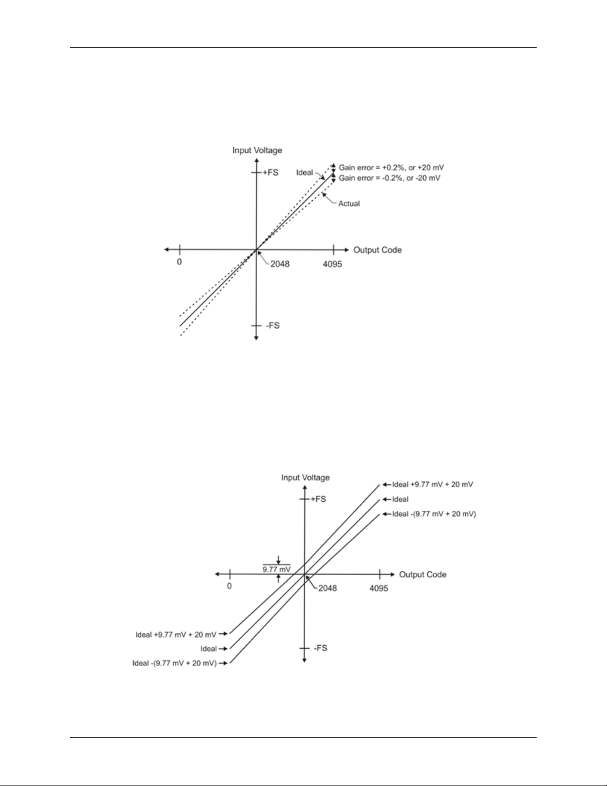
Gain error is a change in the slope of the transfer function from the ideal and is typically expressed as a
percentage of full-scale.
Figure 13 shows the transfer function with gain error. Gain error is easily converted to vol tage by multiplying
the full-scale (
FS) input by the error.
The accuracy plots in Figure 13 are drawn for clarity and are not drawn to scale.
Figure 13. ADC Transfer function with gain error
For example, the USB-1208FS-Plus exhibits a typical calibrated gain error of ±0.2% on all ranges. For the
±10 V range, this would yield 10 V × ±0.002 = ±20 mV. This means that at full scale, and neglecting the effect
of offset, the measurement would be within 20 mV of the actual value. Note that gain error is expressed as a
ratio. Values near ±FS are more affected from an absolute voltage standpoint than are values near mid-scale,
which see little or no voltage error.
Combining these two error sources in Figure 14, we have a plot of the error band for the ±10 V range. This is a
graphical version of the typical accuracy specification of the product.
The accuracy plots in Figure 14 are drawn for clarity and are not drawn to scale.
Figure 14. Error band plot
17

USB-1208FS-Plus User's Guide Functional Details
Synchronized operat ions
You can connect the SYNC pin of two devices together in a master/slave configuration and acquire data from
the analog inputs of both devices using one clock.
When the SYNC pin is configured as an output, the internal A/D pacer clock signal is sent to the screw
terminal. Output the clock signal to the SYNC pin of a second device that is configured for A/D pacer input.
Power
Connecting the device to a computer draws <100 mA of current from the USB +5V supply. When running
applications, the current that c an b e drawn from all device connections (analog, digital, SYNC, and +VO output
loading) is <500 mA. The maximum output current that is available at the +VO p ower output terminal is
100 mA.
With all outputs at their maximum output current, the USB-1208FS-Plus in a fully-loaded configuration may be
above that allowed by the computer. In this case, determine the per-pin loading in the application to ensure that
the maximum loading criteria is met. The per-pin loading is calculated by dividing +5V by the load impedance
of the pin in q uestion.
18

USB-1208FS-Plus User's Guide Functional Details
Mechanical drawings
Figure 15. Circuit board (top) and enclosure dimensions
19

A/D converter type
Successive approximati on type
Input voltage range for linear operation
CHx to GND
Single-ended mode: ±10 V max
Differential mode: –10 V min, +20 V max
Absolute maximum input voltage
CHx to GND
±28 V max
Input impedance
122 kΩ
Input current (Note 1)
Vin = +10 V
70 µA typ
Vin = 0 V
–12 µA typ
Vin = –10 V
–94 µA typ
Input ranges
Single-ended
±10 V, G=2
Differential
±20 V, G=1
Software-selectable
Throughput (Note 2)
Software paced
250 S/s typ, PC-dependent
Hardware paced
0.014 S/s to 50 kS/s
unique and listed in ascending order.
Single-ended
11 bits
Integral linearity error
±1 LSB typ
Differential linearity error
±0.5 LSB typ
Repeatability
±1 LSB typ
Software-selectable
Pacer source
Software-selectable
Internal
Software-selectable
Specifications
All specifications are subject to change without notice.
Typical for 25°C unless otherwise specified.
Specifications in italic text are guaranteed by design.
Analog input
Table 1. Analog input specifications
Parameter Condition Specification
Chapter 4
Number of channels 8 single-ended or 4 differential; software-selectable
±10 V, G=2
±5 V, G=4
±4 V, G=5
±2.5 V, G=8
±2.0 V, G=10
±1.25 V, G=16
±1.0 V, G=20
Channel gain que ue
Resolution (Note 3) Differential 12 bits, no missi ng code s
Trigger source Software-selectable External digital: TRIG_IN
Software selectable. 8 elements in SE mode,
4 elements in DIFF mode.
One gain element per ch annel. Elements must be
External (SYNC), rising edge triggered
Note 1: Input cu rrent is a function of applied voltage on the analog input channels. For a given input voltage, Vin, the
Note 2: M a ximum throughp ut when scanning is machine dependent.
Note 3: The AD7870 converter only returns 11 bits (0 to 2,047 codes) in single-ended mode.
input leakage is approximately equal to (8.181 * V
20
– 12) µA.
in

USB-1208FS-Plus User's Guide Specifications
±20 V
5.1
±10 V
6.1
±5 V
8.1
±4 V
9.1
±2.5 V
12.1
±1.25 V
20.1
±1 V
24.1
±10 V
4.0
±20 V
0.2
40
9.766
49.766
±10 V
0.2
20
9.766
29.766
±5 V
0.2
10
9.766
19.766
±4 V
0.2 8 9.766
17.766
±2.5 V
0.2 5 9.766
14.766
±1.25 V
0.2
2.5
9.766
12.266
±1 V
0.2 2 9.766
11.766
±10 V
0.2
20
19.531
39.531
±20 V
2
0.30
±10 V
2
0.30
±5 V
3
0.45
±4 V
3
0.45
±2.5 V
4
0.61
±2 V
5
0.76
±1.25 V
7
1.06
±1 V
8
1.21
Accuracy
Table 2. Accuracy, differential mode
Range Accuracy (LSB)
±2 V 14.1
Table 3. Accuracy, sing le -ended mode
Range Accuracy (LSB)
Table 4. Accuracy components, differential mode – all values are (±)
Range % of Reading Gain Error at FS (mV) Offset (mV) Accuracy at FS (mV)
±2 V 0.2 4 9.766 13.766
Table 5. Accuracy components, single-en ded mode – all values are (±)
Range % of Reading Gain Error at FS (mV) Offset (mV) Accuracy at FS (mV)
Noise performance
Table 6. Noise performance, differential mode
Range Typical counts LSB
rms
21

USB-1208FS-Plus User's Guide Specifications
±10 V
2
0.30
Output range
0 V to 5.0 V
Software paced
250 S/s single channel typ, PC dependent
Power on and reset voltage
Initializes to 000h code
Output drive
Each D/A OUT
5 mA, sourcing
0 V to 5.0 V
4.0 typ, 45.0 max
(Note 5)
0 V to 5.0 V
0.1 typ, 0.9 max
4.0 typ, 36.0 max
1.0 typ, 9.0 max
4.0 typ, 45.0 max
Table 7. Noise performance, single-ended mode
Range Typical counts LSB
rms
Analog output
Table 8. Analog output specifications
Parameter Condition Specification
Resolution
Number of channels
Throughput (Note 4)
Hardware paced 50 kS/s max per channel
Slew rate
Note 4: M a ximum throughp ut when scanning is machine dependent.
Table 9. Analog output accuracy, all values are (±); accuracy tested at no load
Range Accuracy (LSB)
Table 10. Analog output accuracy components, all values are (±)
12-bits, 1 in 4,096
2
0.8 V/ µs typ
Range % of FSR Gain Error at FS (mV) Offset (mV)
Note 5: Zero-scale offsets may result in a fixed zer o-scale error producing a "dead -band” digital input code region. In
this case, changes in digital input code at values less than 0x040 may not produce a corresponding change in the
output voltage. The offset error is tested and specified at code 0x040.
Accuracy at FS (mV)
22

USB-1208FS-Plus User's Guide Specifications
Digital type
CMOS
Number of I/O
16 (Port A0 through A7, Port B0 through B7)
Configuration
2 banks of 8. Port B is high current drive.
Pull up/pull-down configuration
All pins pulled up to 5V via 47 kΩ resistors (default). Change to pull-down using
internal user-configurable jumpers.
Input high voltage threshold
2.0 V min
Input high voltage limit
5.5 V absolute max
Input low voltage threshold
0.8 V max
Input low voltage limit
–0.5 V absolute min
0 V recommended min
Output high voltage, Port A
4.4 V min (IOH = –20 µA)
Output low voltage, Port A
0.1 V max (IOL = 20 µA)
0.33 V max (IOL = 6.0 mA)
3.76 V min (IOH = –24.0 mA)
0.44 V max (IOH = 24.0 mA)
Power on and reset state
Input
Trigger mode
Edge sensitive; software-selectable for CMOS compati ble rising or falling edge, high
or low level.
Trigger pulse width
1 µs mi n
Input type
Schmitt trigger, 47 kΩ pull-down to gr ou nd
Schmitt trigger hysteresis
1.01 V typ
1.5 V max
3.1 V max
Input high voltage limit
5.5 V absolute max
Input low voltage threshold
1.42 V typ
2.0 V max
0 V recommended min
Digital input/output
Table 11. Digital I/O specifications
Parameter Specification
3.84 V min (IOH = –6. 0 mA)
Output high voltage, Port B 4.4 V min (IOH = –50 µA)
Output low voltage, Port B 0.1 V max (IOH = 50 µA)
External trigger
Table 12. Digital trigger specifications
Parameter Specification
Trigger source External digital; TRIG_IN terminal
Trigger latency 10 µs max
0.6 V min
Input high voltage threshold 2.43 V typ
1.9 V min
1.0 V min
Input low voltage limit –0.5 V absolute min
23

USB-1208FS-Plus User's Guide Specifications
Terminal name
SYNC
Terminal type
Bidirectional
Direction
Output
Outputs the intern al A/D pacer clock
Input (default)
Receives A/D pacer clock from external source
Input clock rate
50 kHz, max
Input mode
1 µs mi n
Output mode
5 µs mi n
Input type
Schmitt trigger, 47 kΩ pull-down to ground
1.5 V max
Input high voltage threshold
2.43 V typ
3.1 V max
Input low voltage threshold
1.42 V typ
2.0 V max
Input low voltage limit
–0.5 V absolute min
0 V recommended min
Output high voltage
4.4 V min (IOH = –50 µA)
3.80 V min (IOH = –8 mA)
Output low voltage
0.1 V max (IOL = 50 µA)
0.44 V max (IOL = 8 mA)
External clock input/output
Table 13. External clock I/O specifications
Parameter Condition Specification
(software-selectable)
Clock pulse width
Schmitt trigger hysteresis 1.01 V typ
0.6 V min
1.9 V min
Input high voltage limit 5.5 V absolute max
1.0 V min
24

USB-1208FS-Plus User's Guide Specifications
Pin name
CTR
Counter type
Event counter
Number of channels
1
Input type
Schmitt trigger, 47 kΩ pull-down to ground, rising edge triggered
Input source
CTR screw terminal
Resolution
32 bits
Maximum input frequency
1 MHz
High pulse width
500 ns min
Low pulse width
500 ns min
Schmitt trigger hysteresis
1.01 V typ
1.5 V max
Input high voltage threshold
2.43 V typ
Input high voltage limit
5.5 V absolute max
Input low voltage threshold
1.42 V typ
2.0 V max
0 V recommended min
Non-volatile EEPROM
2,048 bytes (768 bytes calibration, 256 bytes user, 1,024 bytes DAQFlex)
Type
High performanc e 16-bit RISC microcontroller
Supply current
During USB enumeration
< 100 mA
After USB enumeration, including DIO, AO, SYNC,
and +VO output loading
< 500 mA
+VO power available
After USB enumeration
4.5 V min, 5.25 V max
+VO output current
After USB enumeration
100 mA max
Counter
Table 14. Counter specifications
Parameter Specification
0.6 V min
1.9 V min
3.1V max
1.0 V min
Input low voltage limit –0.5 V absolute min
Memory
Table 15. Memory specifications
Microcontroller
Table 16. Microcontroller specifications
Power
Table 17. Power specifications
Parameter Condition Specification
25

USB-1208FS-Plus User's Guide Specifications
Device type
USB 2.0 full speed
Device compatibility
USB 1.1, USB 2.0
Operating temperature range
0 °C to 70 °C
Storage temperature range
–40 °C to 70 °C
Humidity
0% to 90% non-condensing
Dimensions (L × W × H)
79 × 82 × 27 mm (3.10 × 3.20 × 1.05 in.)
USB cable length
3 m (9.84 ft) max
User connection len gt h
3 m (9.84 ft) max
Connector type
Screw terminal
Wire gauge range
16 AWG to 30 AWG
General
Table 18. General specifications
Parameter Specification
Environmental
Table 19. Environmental speci ficat ion s
Parameter Specification
Mechanical
Table 20. Mechanical specific ation s
Parameter Specification
Signal connector
Table 21. Screw terminal specifications
Parameter Specification
26

USB-1208FS-Plus User's Guide Specifications
Pin
Signal name
Pin description
Pin
Signal name
Pin description
1
CH0 IN HI
Analog input 0+
21
Port A0
Port A bit 0
2
CH0 IN LO
Analog input 0–
22
Port A1
Port A bit 1
3
AGND
Analog ground
23
Port A2
Port A bit 2
4
CH1 IN HI
Analog input 1+
24
Port A3
Port A bit 3
5
CH1 IN LO
Analog input 1–
25
Port A4
Port A bit 4
6
AGND
Analog ground
26
Port A5
Port A bit 5
7
CH2 IN HI
Analog input 2+
27
Port A6
Port A bit 6
8
CH2 IN LO
Analog input 2–
28
Port A7
Port A bit 7
9
AGND
Analog ground
29
GND
Ground
11
CH3 IN LO
Analog input 3–
31
GND
Ground
13
D/A O UT 0
Analog output 0
33
Port B1
Port B bit 1
14
D/A O UT 1
Analog output 1
34
Port B2
Port B bit 2
15
AGND
Analog ground
35
Port B3
Port B bit 3
16
Reserved
Reserved for future use
36
Port B4
Port B bit 4
17
GND
Ground
37
Port B5
Port B bit 5
18
TRIG_IN
Trigger input
38
Port B6
Port B bit 6
19
SYNC
Synchronization I/O
39
Port B7
Port B bit 7
20
CTR
Counter input
40
GND
Ground
Pin
Signal name
Pin description
Pin
Signal name
Pin description
1
CH0 IN
Analog input 0
21
Port A0
Port A bit 0
2
CH1 IN
Analog input 1
22
Port A1
Port A bit 1
3
AGND
Analog ground
23
Port A2
Port A bit 2
4
CH2 IN
Analog input 2
24
Port A3
Port A bit 3
5
CH3 IN
Analog input 3
25
Port A4
Port A bit 4
6
AGND
Analog ground
26
Port A5
Port A bit 5
7
CH4 IN
Analog input 4
27
Port A6
Port A bit 6
8
CH5 IN
Analog input 5
28
Port A7
Port A bit 7
9
AGND
Analog ground
29
GND
Ground
10
CH6 IN
Analog input 6
30
+VO
Power output
11
CH7 IN
Analog input 7
31
GND
Ground
12
AGND
Analog ground
32
Port B0
Port B bit 0
13
D/A O UT 0
Analog output 0
33
Port B1
Port B bit 1
14
D/A O UT 1
Analog output 1
34
Port B2
Port B bit 2
15
AGND
Analog ground
35
Port B3
Port B bit 3
16
Reserved
Reserved for future use
36
Port B4
Port B bit 4
18
TRIG_IN
Trigger input
38
Port B6
Port B bit 6
19
SYNC
Synchronization I/O
39
Port B7
Port B bit 7
20
CTR
Counter input
40
GND
Ground
Differential mode pinout
Table 22. 4-channel differential mode pinout
10 CH3 IN HI Analog input 3+ 30 +VO Power output
12 AGND Analog ground 32 Port B0 Port B bit 0
Single-ended mode pinout
Table 23. 8-channel single-ended mode pinout
17 GND Ground 37 Port B5 Port B bit 5
27

EU Declaration of Conformi ty
According to ISO/IEC 17050-1:2010
Manufacturer: Measurement Computing Corporation
Address: 10 Commerce Way
Norton, MA 02766
USA
Product Category: Electrical equipment for measurement, control and laboratory use.
Date and Place of Issue: July 21, 2016, Norton, Massachusetts USA
Test Report Number: EMI6102.12
Measurement Computing Corporation declares under sole responsibility that the product
USB-1208FS-Plus
is in conformity with the relevant Unio n Harmonization Legislation and co mplies wi th the essential
requirements of the following applicable European Directives:
Electromagnetic Compatibility ( EMC) Directive 2014/30/EU
Low Voltage Directive 2014/3 5/EU
RoHS Directive 2011/65/EU
Conformity is assessed in accordance to the following standards:
EMC:
Emissions:
EN 61326-1:2013 (IEC 61326-1:2012), Class A
EN 55011: 2009 + A1:2010 (IEC CISPR 11:2009 + A1:2010), Group 1, Class A
Immunity:
EN 61326-1:2013 (IEC 61326-1:2012), Controlled EM Environments
EN 61000-4-2:2008 (IEC 61000-4-2:2008)
EN 61000-4-3 :2010 (IEC61000-4-3:2010)
Safety:
EN 61010-1:2010 (IEC 61010-1:2010)
Environmental Affairs:
Articles manufactured on or after the Date of Issue of this Declaration of Conformity do not contain any of the
restricted substances in concentrations/applications not permitted b y the RoHS Directive.
Carl Haapaoja, Director of Quality Assurance

Measurement Computing Corporation NI Hungary Kft
10 Commerce Way H-4031 Debrecen, Hátar út 1/A, Hungary
Norton, Massachusetts 02766 Phone: +36 (52) 515400
(508) 946-5100 Fax: +36 (52) 515414
Fax: (508) 946-9500 http://hungary.ni.com/debrecen
E-mail: info@mccdaq.com
www.mccdaq.com
 Loading...