

Page 1
FFXX1122 BBooaarrdd RReeffeerreennccee MMaannuuaall
FFeeaattuurriinngg tthhee XXiilliinnxx VViirrtteexx--44 FFPPGGAA
Revision: August 2, 2006
www.digilentinc.com
215 E Main Suite D | Pullman, WA 99163
(509) 334 6306 Voice and Fax
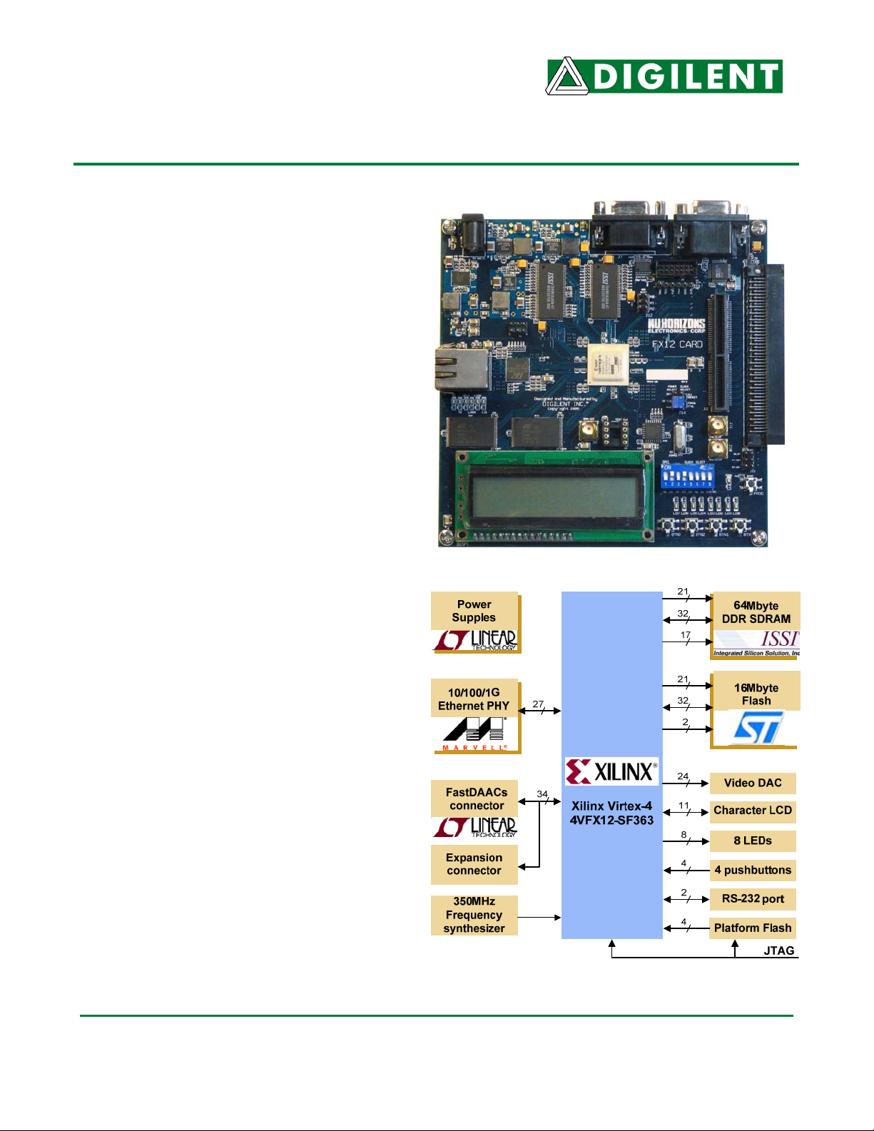
Overview
The Digilent FX12 board (the FX12) is an
integrated circuit development platform for
Xilinx’s Virtex-4 FX12 FPGA. The FX12 is
based on Xilinx’s newest programmable
architecture and contains a PowerPC core,
dual Ethernet MACs, 32 XtremeDSP slices,
80Kbytes of block RAM, advanced clock
management, and flexible I/O’s. The FX12
also features external memories, a flexible
time base, power supplies, an Ethernet PHY,
ports, and other I/O devices.
The FX12 provides an ideal platform for
investigating a new generation of highly
integrated designs made possible by Xilinx’s
Virtex-4 family.
Features include:
• a Virtex-4 FX12 FPGA
• JTAG programming port that can
accommodate all Digilent and Xilinx
programming cables
• XCF08S Xilinx Platform Flash ROM to
store FPGA configurations
• Marvell 88E1111 “Alaska” Gigabit PHY
• 24-bit Analog Devices high-speed Video
DAC
• 64 Mbytes of ISSI DDR SDRAM
• 16 Mbytes of Micron Flash ROM
• high-current Linear Technology
switching power supplies
• Linear Technology FastDAACS
connector for driving high-speed analog
peripherals
• user-settable Integrated Circuit System
frequency synthesizer (up to 350MHz)
• on board serial port, LCD display,
buttons, switches, and LEDs
• high-speed-capable expansion
connector
Doc: 502-108 page 1 of 18
Copyright Digilent, Inc. All rights reserved. Other product and company names mentioned may be trademarks of their respective owners.
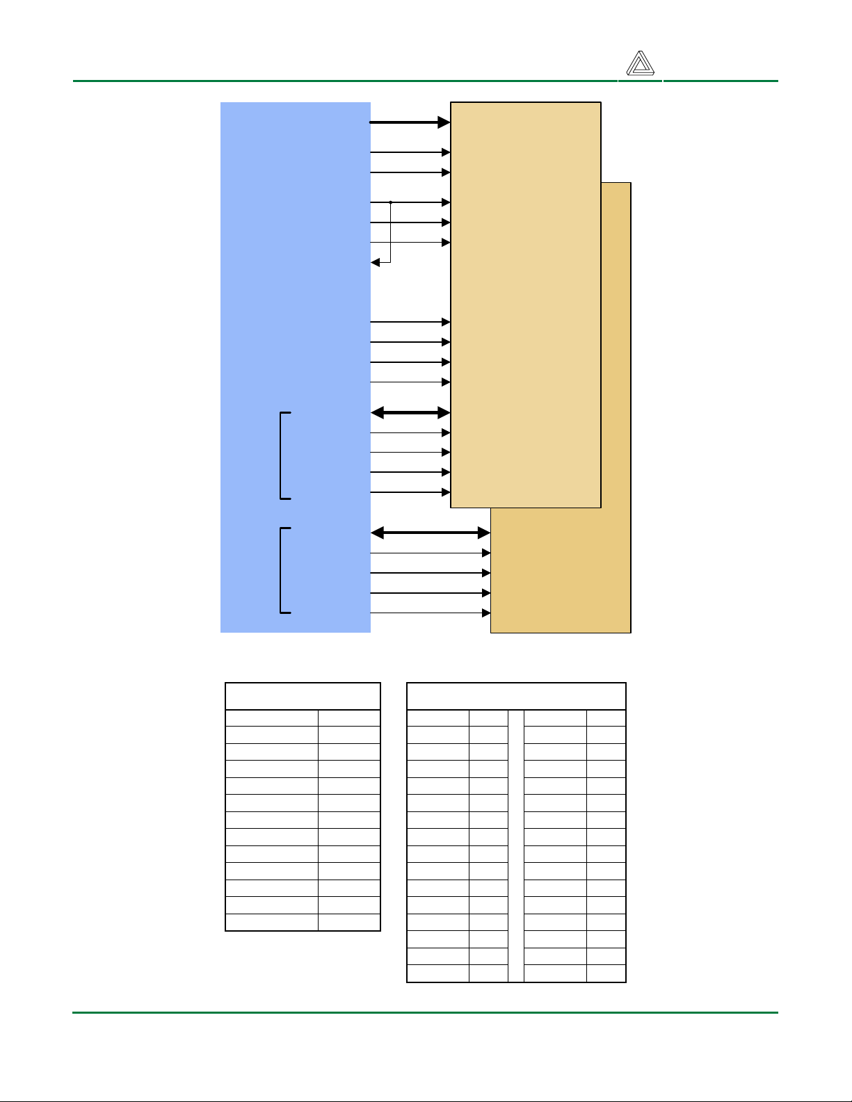
FX12 Block Diagram
®
Page 2
FX12 Reference Manual
Digilent
www.digilentinc.com
Functional Description
The FX12 showcases the many advanced features of Xilinx’s Virtex-4 FPGA, especially its ability to
serve as the single device at the core of an embedded system. The FX12 includes a host of advanced
features, including an embedded PowerPC core, a hard-IP MAC, XtremeDSP slices that include fast
hardware multipliers, advanced clock management, Smart RAM, and other features, bringing new
capabilities to highly-integrated embedded platforms. The FX12 board enhances the abilities of the
FPGA by adding peripheral devices such as 64Mbytes of DDR memory, 16Mbytes of Flash ROM, and
an Ethernet port, making it well suited to support a variety of embedded system designs.
The FX12 is supported by world-class design tools, including ISE, Chipscope-Pro, Embedded
developers Kit (EDK), and System Generator.
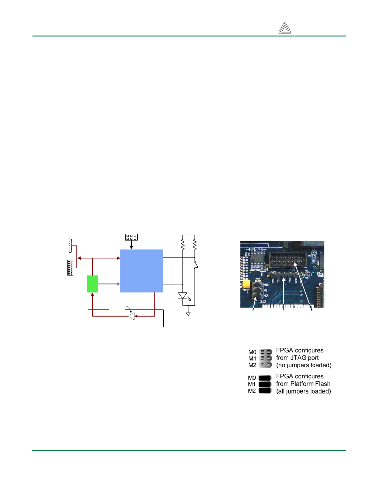
JTAG Ports and Device Configuration
The FX12 can be programmed from a PC or directly from an on-board Flash ROM at power-on. PC
programming requires a programming cable such as Digilent’s JTAG3 or JTAG-USB cable, or Xilinx’s
PC4 or Platform USB cable. Programming files for the Virtex-4 and XCF08 Platform Flash ROM can
be created using Xilinx’s ISE or EDK software, or a variety of other third-party tools. Please refer to
the appropriate CAD tool reference materials for information on creating programming files.
Mode select
JTAG3
header
PC4
header
XCF08
Platform
Flash
jumper
JTAG
Virtex-4
FPGA
Slave
Serial
Bypass
buffer
Hirose FX2 connector
PROG
DONE
LD14
Vdd
PROG (reset)
pushbutton
Mode Select
Jumpers
JTAG3
Connector
PC4
Connector
A .bit file may be programmed into the FPGA from a PC by
setting the mode jumpers to “JTAG” mode, attaching a
programming cable to the PC and to one of the two
programming headers (JTAG3 or PC4), and running Digilent’s
Adept software or Xilinx’s iMPACT programming tool (Adept is a
free download from the Digilent website and iMPACT is a free
download from the Xilinx website). The configuration software
will automatically identify all devices in the scan chain, and allow
Mode Select Jumper Settings
the FPGA and ROM to either be bypassed individually, or
programmed individually with any available .bit or .mcs file. Note that both the FPGA and Platform
Flash ROM will always appear in the scan chain. If a JTAG-aware peripheral board is attached to the
Hirose FX2 expansion connector, it will appear in the scan chain between the FPGA and Platform
Flash.
Copyright Digilent, Inc. Page 2/18 Doc: 502-046
Page 3
FX12 Reference Manual
Digilent
www.digilentinc.com
After the Platform Flash ROM has been loaded with a configuration file, the FPGA can load that file at
power-on if the mode select jumpers are set in the Platform Flash position.
An FPGA system-reset button labeled PROG has been provided to allow a user-initiated FPGA reset.
Pressing the PROG button will clear all configuration memory and cause the FPGA to await the next
programming cycle. An LED on the DONE signal will illuminate at the end of a successful
configuration.
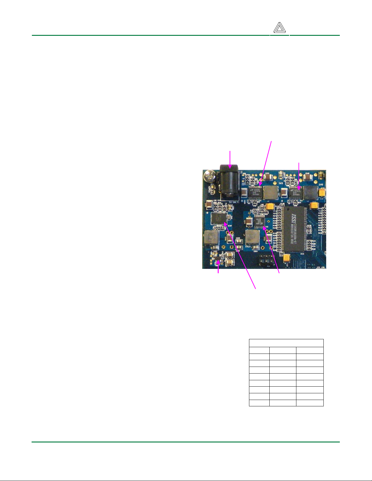
Power Supplies
Power is delivered to the FX12 board via a 2.1mm,
center-positive power connector that can be driven
from any suitable 4VDC-5.5VDC source (like a
2.1mm centerpositive power jack
3.3V switching supply
for FPGA I/O and
peripherals (LTC3416)
2.5V switching supply
for DDR (LTC3416)
wall-plug supply). Power is routed from the
connector to four switching regulators and single
LDO that produce all required supply voltages.
Input power is also routed directly to the character
LCD and high-speed expansion connector (pins
A49 and A50) for use by peripheral circuits.
Current Consumption
Total board current is dependant on FPGA
configuration, synthesizer clock frequency, and
external connections. In test configurations using
the PPC core to run DDR and Flash memory tests,
with roughly 10% of the FPGA routed and a
100MHz input clock, approximately 650mA of
supply current is drawn from the main power
supply. Required current will increase if larger
circuits are configured in the FPGA, if clock
frequency is increased, and if peripheral boards are
attached.
1.8V LDO for
Platform Flash
ROM (LTC1844)
FX12 Power Supplies
1.25V switching supply for
DDR termination (LTC3413)
1.2V switching supply for
FPGA core (LTC3418)
Power Distribution
The FX12 uses an eight-layer PCB, with the stack-up shown in the
table. The Vdd planes are split into several localized islands to
accommodate the various component’s supply voltage requirements.
Bulk ceramic bypass capacitors are placed strategically around the
board, and every component Vdd pin has one, two, or three local
bypass caps in the .001 to .047uF range. The power supply routing
and bypass capacitors result in a very clean low-noise power supply.
FX12 Stack-Up
Layer Usage Copper
1 Signal 1 oz.
2 GND .5 oz.
3 Signal .5 oz.
4 Vdd .5 oz.
5 Vdd .5 oz.
6 Signal .5 oz.
7 GND .5 oz.
8 Signal 1 oz.
Supply Details
Copyright Digilent, Inc. Page 3/18 Doc: 502-046
Page 4
FX12 Reference Manual
Regulator
Part
Number
Supply
Max
Current
• Hirose expansion connector
• Xilinx FPGA I/O banks 2, 4, 6, 7,
and 8
3.3V 4A LTC3416
• Micron Flash memory
• RS-232 level shifter
• Analog Devices Video DAC
• ICS frequency synthesizer
• Xilinx Platform Flash
• Xilinx FPGA I/O banks 1, 3, 5, 7,
2.5V 4A LTC3416
and 8
• ISSI DDR DRAM’s
• Marvell 88E1111 Ethernet PHY
1.8V 150mA LTC1844
1.25V 2A LTC3413
1.2V 8A LTC3418
• Xilinx Platform Flash
• DDR termination networks
• Xilinx FPGA core
• Marvell PHY core
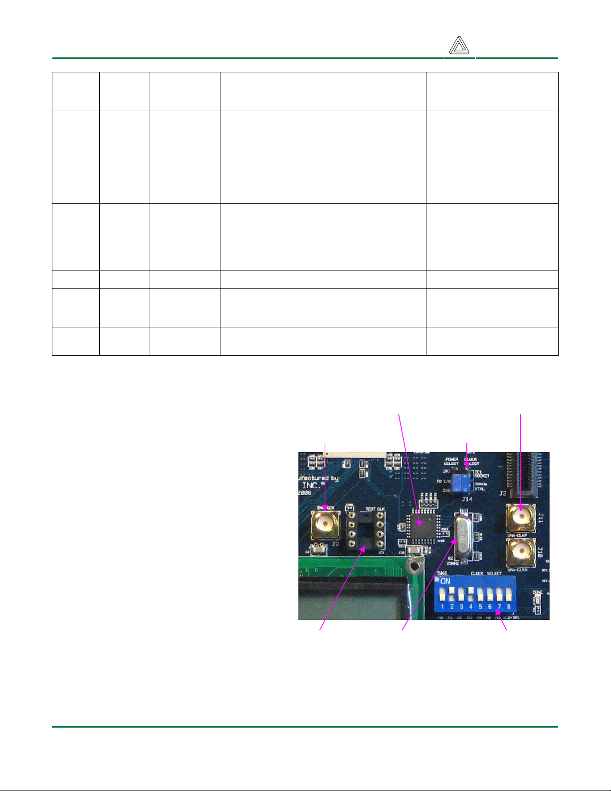
Oscillator
The FX12 includes a 350MHz, crystal-toLVCMOS frequency synthesizer from
Integrated Circuit Systems Inc (PN
ICS8402). The synthesizer gets its primary
frequency input from a 25MHz crystal, and
then multiplies that input up to the desired
output frequency. The output frequency is
selected by the DIP switches at SW1,
according to the table in Appendix A. The
clock output from the synthesizer is
delivered to the FPGA on the GCLK0 input
at pin Y5.
A secondary input is also available to drive
a different base frequency into the
synthesizer. The socket labeled “test_clk”
can accommodate any 12-40MHz LVCMOS
oscillator in a half-DIP package. This
secondary source will drive the synthesizer
if the XTAL_SEL signal is driven high from
the FPGA. The oscillator circuit is shown in
the accompanying figure. Please see the
ICS8402 data sheet for further information.
Digilent
www.digilentinc.com
Devices Powered Notes
Uses oversized 3.3uH
inductor for stability at
low current.
Uses oversized 3.3uH
inductor for stability at
low current.
Uses oversized 1.5uH
inductor for stability at
low current.
SMA Clock
Inputs to FPGA
Frequency Select
Switches
SMA Clock
Output
Secondary
Clock Input
Frequency
Synthesizer
Clock Source
Select Jumper
Primary Crystal
(25MHz)
FX12 Oscillator Circuit
Copyright Digilent, Inc. Page 4/18 Doc: 502-046
Page 5
FX12 Reference Manual
Digilent
www.digilentinc.com
Frequency
Select
Switches
M0
M1
IC15
XTAL_SEL
Q1
M2
M3
M4
N0
ICS8402
Frequency
Synthesizer
N1
VCO_SEL
Q0
OE1
OE2
M5
TEST_CLK
M6
M7
M8
NP_LOAD
XTAL1
XTAL2
MR
FX12 Frequency Synthesizer Diagram
R18 (GCLK0)
R18
Virtex-4
FPGA
SMA
Connector
Test
Clock
Socket
25MHz
Crystal
DDR
The 64Mbyte DDR memory array consists of two 32Mbyte (16M x 16) ISSI IS43R16160A-6T devices
connected as a 16M x 32 array. Individual byte selects for both memories are brought to the FPGA so
byte, word, and long-word read/writes are possible. A differential clock is routed from the FPGA to the
memories, and a length-matched clock return is routed back to the FPGA to allow for timing
optimization. All data signals are delay and impedance matched (with 48-ohm trace impedance), and
all DDR signals are actively terminated through 47-ohm resistors to a 1.25V supply for optimal bus
performance.
UCF File
Signals routed to the DDR SDRAM should use the SSTL2_I standard as shown in the example .ucf
file entry below. All VREF pins on Bank 5 (used by the DDR signal connections) should have “prohibit”
constraints in the .ucf file to prohibit software from assigning these pins to other functions.
NET “DDR_D0” LOC = “P20” | IOSTANDARD = SSTL2_I ;
CONFIG PROHIBIT = C17;
Copyright Digilent, Inc. Page 5/18 Doc: 502-046
Page 6
FX12 Reference Manual
See table
ADDR(12:0)
IC11
Digilent
www.digilentinc.com
BA1
BA0
CK
CK_N
CKE
Dual ISSI
IS43R16160A
DDR SDRAM’s
IC12
Virtex-4
FPGA
C18
D17
P16
P17
N16
B7
DDRCLK
LOOP
(16Mbyte x 16)
D18
F17
E18
F18
See table
IC11
only
J19
N18
A13
B13
See table
IC12
only
A15
B15
A14
B14
FX12 DDR Circuit Diagram
CS
CAS
RAS
WE
DATA(15:0)
LDQS1
UDQS1
LDM1
UDM1
DATA(31:16)
LDQS2
UDQS2
LDM2
UDM2
DDR Address Pins DDR Data Pins
ADDR12 M15 DATA31 H18 DATA15 G17
ADDR11 M16 DATA30 H20 DATA14 H17
ADDR10 F16 DATA29 G20 DATA13 J17
ADDR9 K17 DATA28 G19 DATA12 J18
ADDR8 K16 DATA27 F20 DATA11 K18
ADDR7 J15 DATA26 F19 DATA10 M18
ADDR6 J16 DATA25 E20 DATA9 M17
ADDR5 H16 DATA24 D19 DATA8 N17
ADDR4 G16 DATA23 A16 DATA7 K20
ADDR3 C15 DATA22 B16 DATA6 K19
ADDR2 C16 DATA21 B17 DATA5 L20
ADDR1 D16 DATA20 A18 DATA4 M19
ADDR0 E16 DATA19 B18 DATA3 M20
DATA18 B19 DATA2 N19
DATA17 C19 DATA1 P19
DATA16 C20 DATA0 P20
Copyright Digilent, Inc. Page 6/18 Doc: 502-046
Page 7

FX12 Reference Manual
Digilent
www.digilentinc.com
Flash Memory
The FX12 contains two Micron M29W64OD 4Mbyte Flash devices, for a total of 8Mbytes. The Flash
array is organized as a 2M x 32 array, with all control signals routed in parallel to the two devices.
FX12 Flash Circuit Diagram
Flash Address Pins Flash Data Pins
ADDR21 H3 ADDR10 D3 DATA31 A6 DATA15 H2
ADDR20 G4 ADDR9 E3 DATA30 A5 DATA14 J2
ADDR19 F3 ADDR8 F4 DATA29 B4 DATA13 K1
ADDR18 J4 ADDR7 K4 DATA28 B3 DATA12 L1
ADDR17 J3 ADDR6 K3 DATA27 C2 DATA11 M2
ADDR16 C6 ADDR5 L4 DATA26 D2 DATA10 F5
ADDR15 C5 ADDR4 M3 DATA25 E1 DATA9 H5
ADDR14 D5 ADDR3 M4 DATA24 F1 DATA8 J5
ADDR13 C4 ADDR2 L5 DATA23 B6 DATA7 H1
ADDR12 D4 ADDR1 M5 DATA22 B5 DATA6 K2
ADDR11 C11 ADDR0 M6 DATA21 A3 DATA5 L2
DATA20 B2 DATA4 M1
DATA19 C1 DATA3 E5
DATA18 E2 DATA2 G5
DATA17 F2 DATA1 J6
DATA16 G2 DATA0 K5
VGA Port
The five standard VGA signals Red, Green, Blue, Horizontal Sync (HS), and Vertical Sync (VS)
available at the VGA connector arise from the FPGA (sync signals) and an Analog Devices ADV7125
high speed video DAC (color signals). The video DAC presents three parallel 8-bit data ports to the
Copyright Digilent, Inc. Page 7/18 Doc: 502-046
Page 8

FX12 Reference Manual
Digilent
www.digilentinc.com
FPGA, and the inputs to those ports determine the corresponding color signal voltage delivered to the
VGA connector. The sync signals must be produced by a controller residing in the FPGA.
VGA signal timings are specified,
published, copyrighted and sold by the
VESA organization (www.vesa.org). The
following VGA system timing information
is provided as an example of how a
VGA monitor might be driven in 640 by
480 mode. For more precise
information, or for information on higher
VGA frequencies, refer to
documentation available at the VESA
website.
See table
See table
See table
Virtex-4
FPGA
V16
V15
RED(7:0)
GREEN(7:0)
BLUE(7:0)
CLK
BLANK
Analog Devices
ADV7125 Video
DAC
IC16
R
R_N
G
G_N
B
B_N
RED
GRN
BLU
HS
VS
HD-DB15
PSAVE
RST
SYNC
V6
V5
FX12 VGA Circuit Diagram
RED GREEN BLUE
RED7 V8 GREEN7 W10 BLUE75 W6
RED6 U9 GREEN6 Y11 BLUE6 W5
RED5 V9 GREEN5 W11 BLUE5 W7
RED4 V10 GREEN4 Y12 BLUE4 Y7
RED3 V11 GREEN3 W12 BLUE3 W8
RED2 V12 GREEN2 W13 BLUE2 W9
RED1
RED0 V13 GREEN0 U8 BLUE0 Y10
U1
GREEN1 T7 BLUE1 Y9
Copyright Digilent, Inc. Page 8/18 Doc: 502-046
Page 9

FX12 Reference Manual
Digilent
www.digilentinc.com
VGA System Timing
CRT-based VGA displays use amplitude-modulated moving electron beams (or cathode rays) to
display information on a phosphor-coated screen. LCD displays use an array of switches that can
impose a voltage across a small amount of liquid crystal, thereby changing light permitivity through
the crystal on a pixel-by-pixel basis. Although the following description is limited to CRT displays, LCD
displays have evolved to use the same signal timings as CRT displays (so the “signals” discussion
below pertains to both CRTs and LCDs). Color CRT displays use three electron beams (one for red,
one for blue, and one for green) to energize the phosphor that coats the inner side of the display end
of a cathode ray tube (see illustration). Electron beams emanate from “electron guns”, which are
finely-pointed heated cathodes placed in close proximity to a positively charged annular plate called a
“grid”. The electrostatic force imposed by the grid pulls rays of energized electrons from the cathodes,
and those rays are fed by the current that flows into the cathodes. These particle rays are initially
accelerated towards the grid, but they soon fall under the influence of the much larger electrostatic
force that results from the entire phosphor-coated display surface of the CRT being charged to 20kV
(or more). The rays are focused to a fine beam as they pass through the center of the grids, and then
Anode (entire screen)
Cathode ray tube
Deflection coils
Grid
Cathode ray
Cathode Ray Tube
Display System
Electron guns
(Red, Blue, Green)
R,G,B signals (to guns)
VGA cable
High voltage
supply (>20kV)
deflection
control
grid
control
gun
control
Sync signals
(to deflection control)
they accelerate to impact on the phosphor-coated display surface. The phosphor surface glows
brightly at the impact point, and the phosphor continues to glow for several hundred microseconds
after the beam is removed. The larger the current fed into the cathode, the brighter the phosphor will
glow.
Between the grid and the display surface, the beam passes through the neck of the CRT where two
coils of wire produce orthogonal electromagnetic fields. Because cathode rays are composed of
charged particles (electrons), they can be deflected by these magnetic fields. Current waveforms are
passed through the coils to produce magnetic fields that interact with the cathode rays and cause
them to transverse the display surface in a “raster” pattern, horizontally from left to right and vertically
from top to bottom. As the cathode ray moves over the surface of the display, the current sent to the
electron guns can be increased or decreased to change the brightness of the display at the cathode
ray impact point.
Copyright Digilent, Inc. Page 9/18 Doc: 502-046
Page 10

FX12 Reference Manual
Digilent
www.digilentinc.com
Information is only displayed when the beam is moving in the “forward” direction (left to right and top
to bottom), and not during the time the beam is reset back to the left or top edge of the display. Much
of the potential display time is therefore lost in “blanking” periods when the beam is reset and
stabilized to begin a new horizontal or vertical display pass. The size of the beams, the frequency at
which the beam can be traced across the display, and the frequency at which the electron beam can
be modulated determine the display resolution. Modern VGA displays can accommodate different
resolutions, and a VGA controller circuit dictates the resolution by producing timing signals to control
the raster patterns. The controller must produce synchronizing pulses at 3.3V (or 5V) to set the
frequency at which current flows through the deflection coils, and it must ensure that video data is
applied to the electron guns at the correct time. Raster video displays define a number of “rows” that
corresponds to the number of horizontal passes the cathode makes over the display area, and a
number of “columns” that corresponds to an area on each row that is assigned to one “picture
element” or pixel. Typical displays use from 240 to 1200 rows and from 320 to 1600 columns. The
overall size of a display and the number of rows and columns determines the size of each pixel.
Video data typically comes from a video refresh memory, with one or more bytes assigned to each
pixel location (the FX12 uses 8-bits per pixel). The controller must index into video memory as the
beams move across the display, and retrieve and apply video data to the display at precisely the time
the electron beam is moving across a given pixel.
pixel 0,0
pixel 0,639
A VGA controller circuit
must generate the HS and
VS timings signals and
640 pixels are displayed each
time the beam travels across
the screen
coordinate the delivery of
video data based on the
pixel clock. The pixel clock
defines the time available
Current
through
horizontal
defletion
coil
VGA display
surface
pixel 479,0 pixel 479,639
Stable current ramp - information
displayed during this time
Retrace - no
information
displayed
during this
time
to display one pixel of
information. The VS signal
defines the “refresh”
frequency of the display,
or the frequency at which
all information on the
display is redrawn. The
minimum refresh
frequency is a function of
the display’s phosphor and
electron beam intensity,
with practical refresh
time
Total horizontal time
Horizontal display time
retrace
time
frequencies falling in the
50Hz to 120Hz range. The
number of lines to be
displayed at a given
HS
Horizontal sync signal
sets retrace frequency
"back porch""front porch"
refresh frequency defines
the horizontal “retrace”
frequency. For a 640-pixel
by 480-row display using a 25MHz pixel clock and 60 +/-1Hz refresh, the signal timings shown in the
table below can be derived. Timings for sync pulse width and front and back porch intervals (porch
intervals are the pre- and post-sync pulse times during which information cannot be displayed) are
based on observations taken from actual VGA displays.
Copyright Digilent, Inc. Page 10/18 Doc: 502-046
Page 11

FX12 Reference Manual
Digilent
www.digilentinc.com
A VGA controller circuit decodes the output of a horizontal-sync counter driven by the pixel clock to
generate HS signal timings. This counter can be used to locate any pixel location on a given row.
Likewise, the output of a vertical-sync counter that increments with each HS pulse can be used to
generate VS signal timings, and this counter can be used to locate any given row. These two
continually running counters can be used to form an address into video RAM. No time relationship
between the onset of the HS pulse and the onset of the VS pulse is specified, so the designer can
arrange the counters to easily form video RAM addresses, or to minimize decoding logic for sync
pulse generation.
Symbol Parameter
T
Sync pulse time
S
T
Display time
disp
T
VS pulse width
pw
T
VS front porch
fp
T
VS back porch
bp
Vertical Sync
Time Clocks Lines
16.7ms
15.36ms
320 us
928 us
64 us
416,800
384,000
1,600
8,000
23,200
Horizontal Sync
Time
521
480
10
29
2
32 us
25.6 us
3.84 us
640 ns
1.92 us
Clocks
800
640
96
16
48
T
S
T
disp
T
pw
T
fp
T
bp
Signal Timings
LCD
The FX12 contains a 16x2 character LCD manufactured by PowerTip (PN 1602D – see
www.powertip.com.tw
and Sitronix ST7066U devices. All pins are routed directly to the Virtex FPGA as shown below.
the associated character to appear at the corresponding display location. Display positions can be
shifted left or right by setting a bit in the instruction register (IR). The write-only IR directs display
operations (such as clear display, shift left or right, set DDRAM address, etc). Available instructions
(and the associated IR codes) are shown in the right-most column of the “LCD Instructions and
Codes” table below. A busy flag shows whether the display has competed the last requested
operation; prior to initiating a new operation, the flag can be checked to see if the previous operation
has been completed.
The display has more DDRAM locations than can be displayed at any given time. DDRAM locations
00H to 27H map to the first display row, and locations 40H to 67H map to the second row. Normally,
DDRAM location 00H maps to the upper left display corner, and 40H to the lower left. Shifting the
display left or right can change this mapping. The display uses a temporary data register (DR) to hold
data during DDRAM /CGRAM reads or writes, and an internal address register to select the RAM
location. Address register contents, set via the IR, are automatically incremented after each read or
write operation. The LCD display uses ASCII character codes. Codes up through 7F are standard
). The display uses an LCD controller IC compatible with the Samsung KS066U
The LCD controller contains a charactergenerator ROM (CGROM) with 208 preset 5x8
character patterns, a character-generator RAM
(CGRAM) that can hold eight user-defined 5x8
characters, and a display data RAM (DDRAM)
that can hold 80 character codes. Character
codes written into the DDRAM serve as indexes
into the CGROM (or CGRAM). Writing a character
code into a particular DDRAM location will cause
Copyright Digilent, Inc. Page 11/18 Doc: 502-046
Page 12
FX12 Reference Manual
Digilent
www.digilentinc.com
ASCII (which includes all “normal” alphanumeric characters). Codes above 7F produce various
international characters – please see the manufacturers data sheet for more information on
international codes.
The display is connected to the FX12 board by a 16-pin connector (pins 15 and 16 are for an optional
backlight, and they are not used). The 14-pin interface includes eight data signals, three control
signals, and three voltage supply signals. The eight data bus signals are passed through the CPLD
to/from the system bus for read/write cycles directed to the LCD memory space (address 10X). The
three LCD control signals are driven from the CPLD: the RS (Register Strobe) signal clocks data into
registers, the R/W signal determines bus direction, and the E signal enables the bus for read or write
operations. In the standard CPLD configuration, the R/S and R/W signals are connected to ADDR0
and WE respectively. The E signal can be driven directly from the LCDEN signal available on the
system connector, or if LCDEN is left at logic ‘0’, then E is driven whenever address “10X” is present
on the bus, CS is asserted, and AS or DS are low. LCD bus signals and timings are illustrated below.
LCD Instructions and Codes
Instruction
Clear
Display
Return
Home
Entry Mode
Set
Display
ON/OFF
Control
Cursor or
Display Shift
Function Set 0 0 0 0 1 DL N F X X
Set CGRAM
Address
Set DDRAM
Address
Read Busy
Flag/ Address
Write Data
to RAM
Read Data
from RAM
RS R/W DB7 DB6 DB5 DB4 DB3 DB2 DB1 DB0
0 0 0 0 0 0 0 0 0 1
0 0 0 0 0 0 0 0 1 X
0 0 0 0 0 0 0 1 I/D SH
0 0 0 0 0 0 1 D C B
0 0 0 0 0 1 S/C R/L X X
0 0 0 1 AC5 AC4 AC3 AC2 AC1 AC0 Set CGRAM address counter.
0 0 1 AC6 AC5 AC4 AC3 AC2 AC1 AC0 Set DDRAM address counter.
0 1 BF AC6 AC5 AC4 AC3 AC2 AC1 AC0
1 0 D7 D6 D5 D4 D3 D2 D1 D0
1 1 D7 D6 D5 D4 D3 D2 D1 D0
Instruction Bit Assignments
Description
Clear display by writing a 20H to
all DDRAM locations, set DDRAM
address register to 00H, and
return cursor to home.
Return cursor to home (upper left
corner), and set DDRAM address
to 0H. DDRAM contents not
changed.
I/D = ‘1’ for right-moving cursor
and address increment, SH = ‘1’
for display shift (direction set by
I/D bit).
Set display (D), cursor (C), and
blinking cursor (B) on or off.
SC = ‘0’ to shift cursor right or left,
‘1’ to shift entire display right or
left (R/L = ‘1’ for right).
Set interface data length (DL = ‘1’
for 8 bit), number of display lines
(N = ‘1’ for 2 lines), display font (F
= ‘0’ for 5x 8 dots).
Read busy flag and address
counter.
Write data into DDRAM or
CGRAM, depending on which
address was last set.
Read data from DDRAM or
CGRAM, depending on which
address was last set.
Copyright Digilent, Inc. Page 12/18 Doc: 502-046
Page 13
FX12 Reference Manual
Digilent
www.digilentinc.com
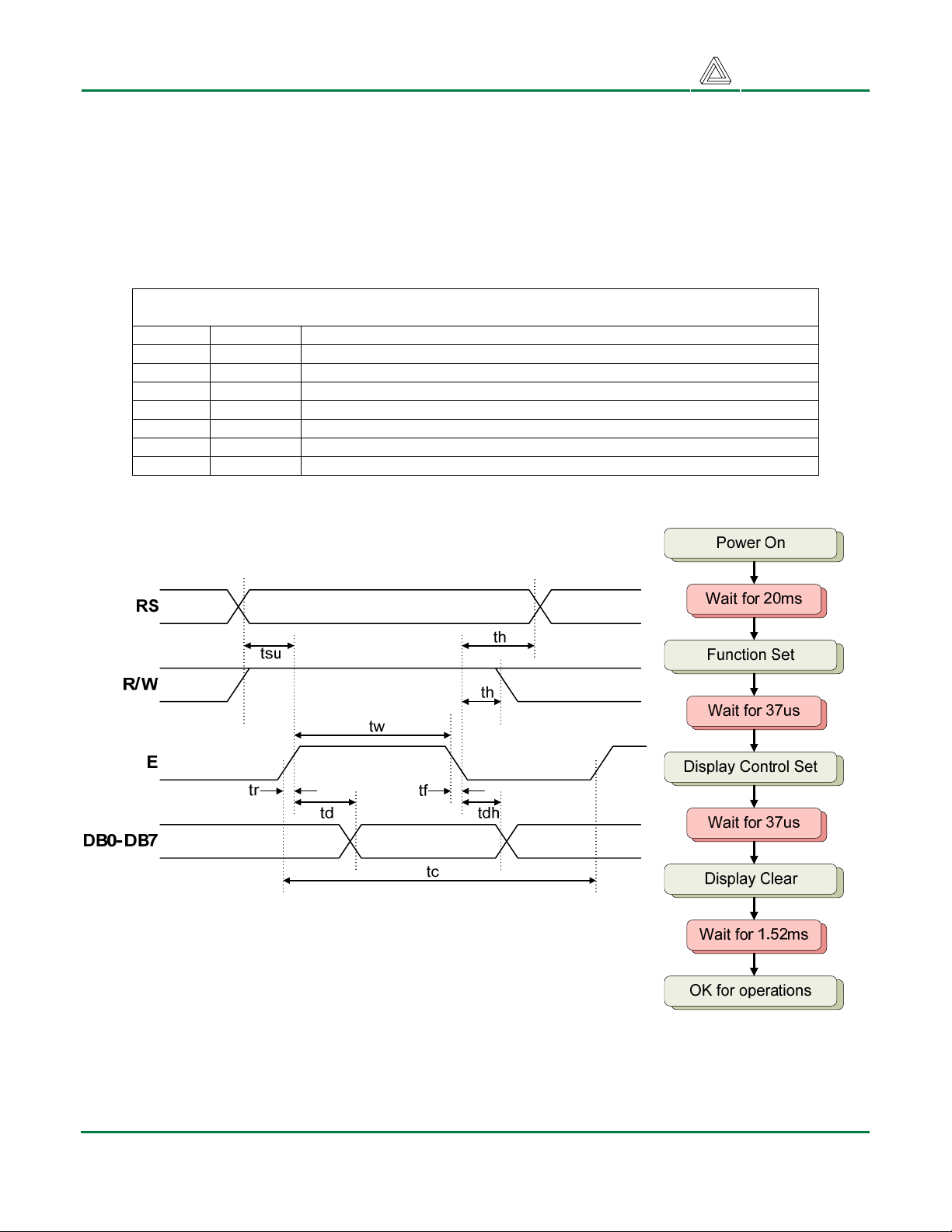
A startup sequence with specific timings ensures proper LCD operation. After power-on, at least 20ms
must elapse before the function-set instruction code can be written to set the bus width, number of
lines, and character patterns (8-bit interface, 2 lines, and 5x8 dots are appropriate). After the functionset instruction, at least 37us must elapse before the display-control instruction can be written (to turn
the display on, turn the cursor on or off, and set the cursor to blink or no blink). After another 37us, the
display-clear instruction can be issued. After another 1.52ms, the entry-mode instruction can set
address increment (or address decrement) mode, and display shift mode (on or off). After this
sequence, data can be written into the DDRAM to cause information to appear on the display.
LCD Connector Signals
Pin No. Symbol Signal Description
1 Vss Signal ground
2 Vdd Power supply (5V)
3 Vo Operating (contrast) voltage (LCD drive, typically 100mV at 20C)
4 RS Register select: high for data transfer, low for instruction register
5 R/W Read/write signal: high for read mode, low for write mode
6 E Read/write strobe: high for read OE; falling edge writes data
7-14 Data Bus Bidirectional data bus
LCD Read Cycle
Copyright Digilent, Inc. Page 13/18 Doc: 502-046
LCD Startup Sequence
Page 14

FX12 Reference Manual
LCD Write Cycle
RS
tsu
th
Digilent
www.digilentinc.com
R/W
tw
tf
th
E
tr
tsu1 th1
DB0-DB7
tc
Parameter Symbol Min Max Unit Test Pin
Enable cycle time tc 500 ns E
Enable High pulse width tw 220 ns E
Enable rise/fall time tr, tf 25 ns E
RS, R/W setup time tsu 40 ns RS, R/W
RS, R/W hold time th 10 ns RS, R/W
Read data output delay td 60 120 ns DB0-DB7
Read data hold time tdh 20 ns DB0-DB7
Write data setup time tsu1 40 ns DB0-DB7
Write data hold time th1 10 ns DB0-DB7
LCD Bus Timings
The LCD connections to the Virtex-4 are shown below. Note the LCD uses a 4-bit data interface, and
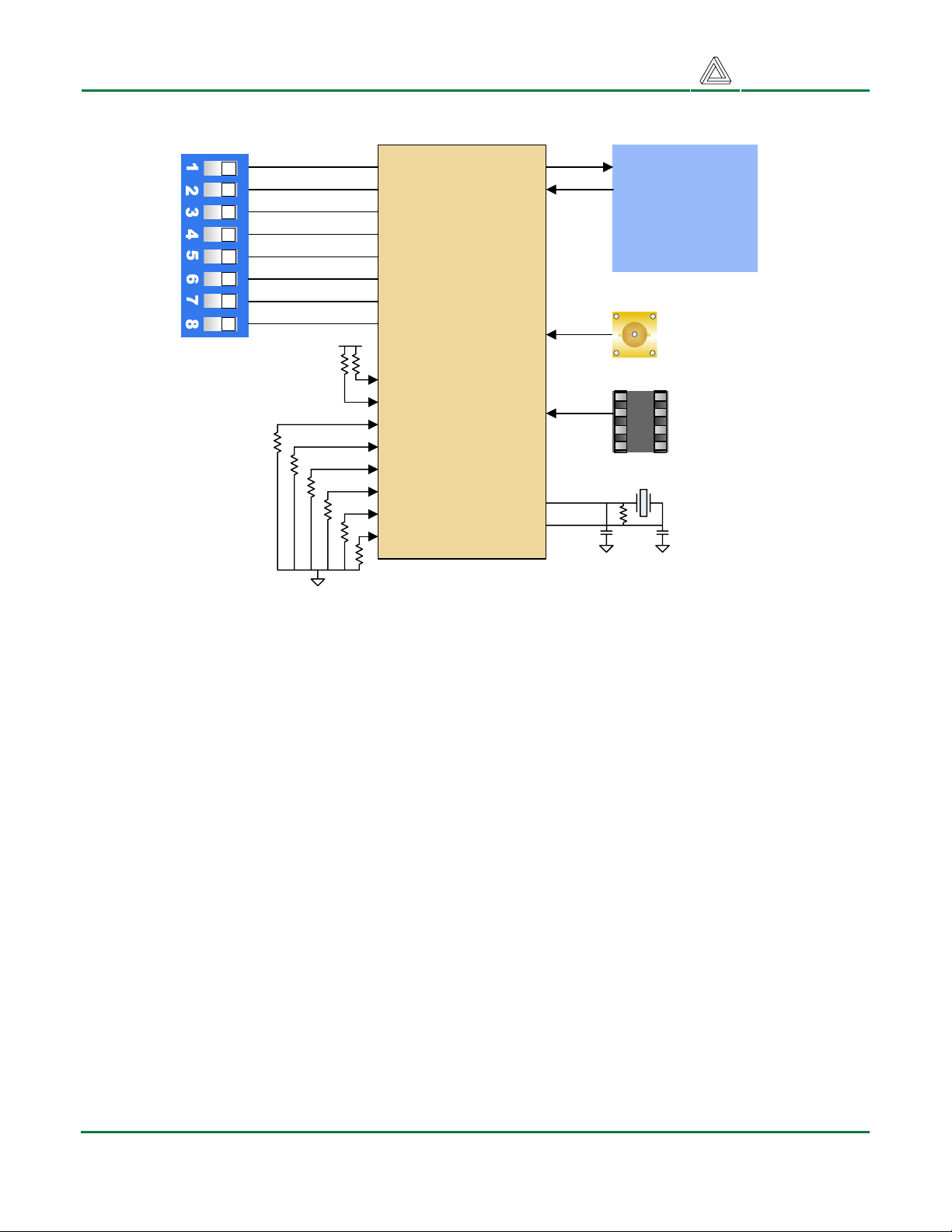
the same FPGA pins that connect to the data bus are shared with the pushbutton inputs.
FX12 LCD Circuit Diagram
Serial Port
The FX12 provides an RS-232 based serial port for user data transfers and embedded processor debug
operations. RS-232 level translation is provided by an Intersil ICL3232 transceiver.
Copyright Digilent, Inc. Page 14/18 Doc: 502-046
Page 15

FX12 Reference Manual
Digilent
www.digilentinc.com
FX12 Serial Port Circuit Diagram
Other User I/O
Eight LEDs, four pushbuttons, and two SMA connectors are provided for general user I/O. Pushbutton
inputs are normally low, and they are driven high only when the pushbutton is pressed. Anodes of the
high-bright LEDs are connected to FPGA pins, so that a logic high signal will illuminate them with just
3-4mA of current. Separate LEDs are provided for power-on indication and successful completion of
FPGA configuration. The two SMA connectors provide a differential pair of I/O’s suitable for highfrequency signals such as clocks.
LD0
U2
LD1
SMA connectors
for (differential)
clock inputs
4 Pushbuttons
8 LEDs
Virtex-4
FPGA
U3
T3
T4
R5
R6
R3
R4
N2
P5
P4
P2
LD2
LD3
LD4
LD5
LD6
LD7
BTN0
BTN1
BTN2
BTN3
User
LEDs
User
Pushbuttons
R2
SMA
CLKP
CLKN
Connectors
R1
User I/O Devices Circuit Diagram
Copyright Digilent, Inc. Page 15/18 Doc: 502-046
Page 16
FX12 Reference Manual
Digilent
www.digilentinc.com
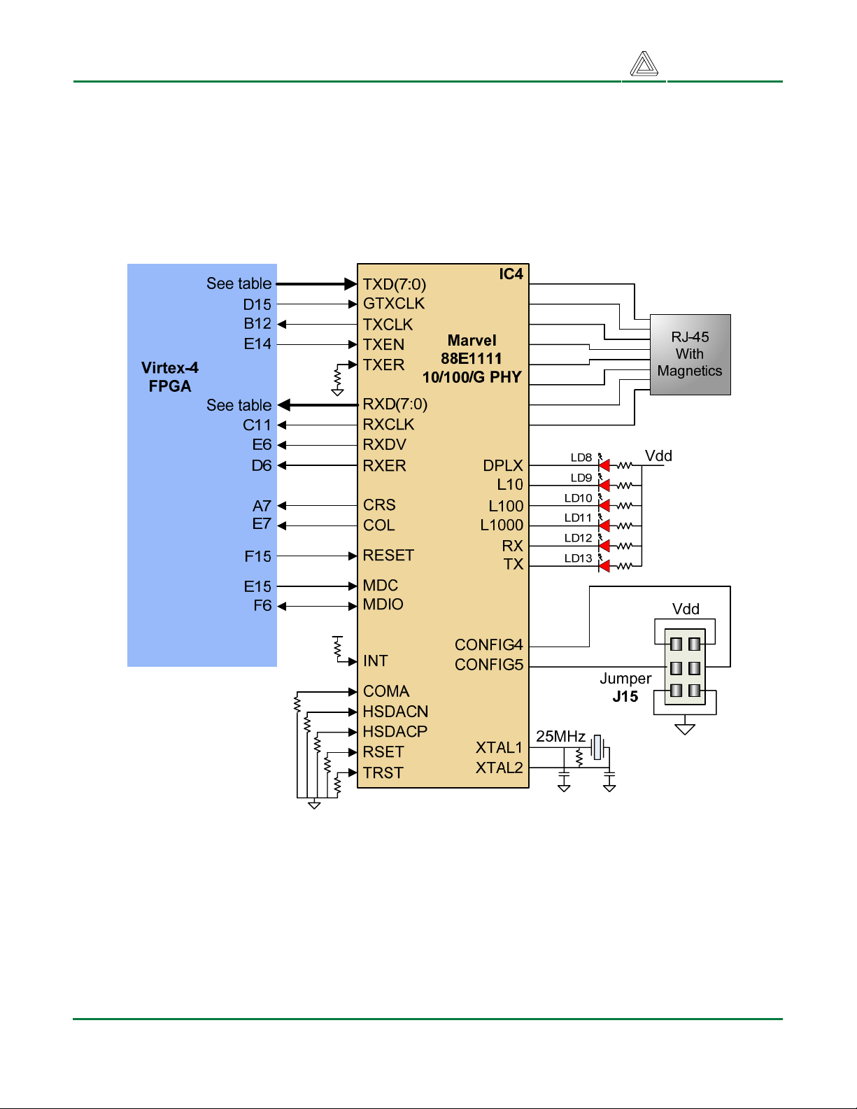
Marvell Ethernet Transceiver
The FX12 board includes a Marvell 10/100/1G Ethernet Transceiver (the “PHY”). The Virtex-4
contains a hard-IP Ethernet MAC that can directly drive the Marvell PHY, or a soft-IP MAC can be
programmed into available gates in the Virtex-4 fabric.
Marvell maintains tight control of their data sheets. For further information on the Marvell PHY, please
contact NuHorizons for assistance with entering into a non-disclosure agreement with Marvell.
FX12 Marvel PHY Circuit Diagram
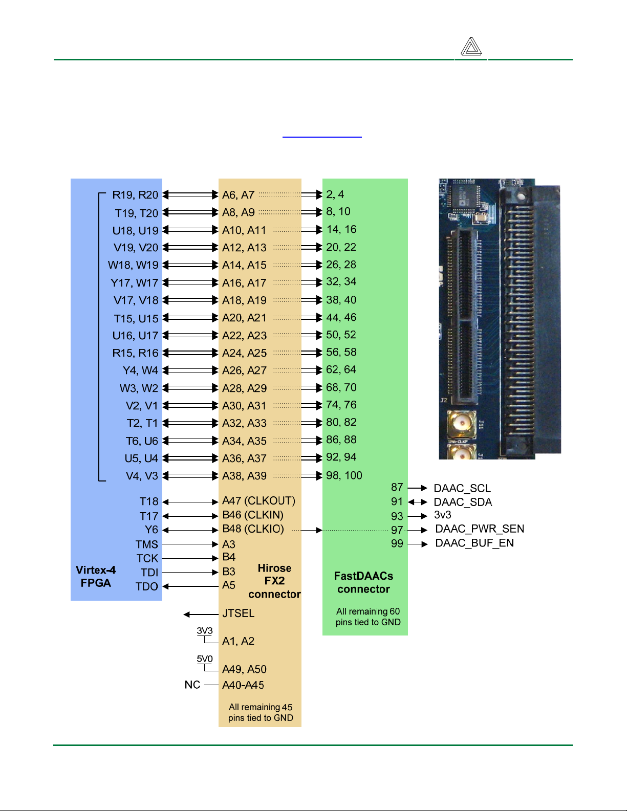
Expansion Connectors
The FX12 provides two primary expansion connectors: a Hirose 100-pin FX2 high-density board-toboard or board-to-cable connector and a second connector that can accommodate FastDAACS A/D
and D/A demo boards from Linear Technology. The FX2 connector includes 17 matched pairs of I/O
signals from the FPGA (34 total signals), as well as the JTAG programming signals and three clock
signals (which can also be used as general I/O’s). Mating board or cable connectors can readily be
Copyright Digilent, Inc. Page 16/18 Doc: 502-046
Page 17
FX12 Reference Manual
Digilent
www.digilentinc.com
obtained from several catalog distributors (see for example the mating part number FX2-100S-1.27DS
available from Digikey).
The 100-pin FastDAACS connector supports direct connection of a number of A/D and D/A sample
boards produced by Linear Technology (see www.linear.com
for more information). The FastDAACs
connector shares the 17 matched pairs of FPGA I/Os with the Hirose Expansion connector, plus five
control signals that constitute Linear Technology’s FastDAACs serial control bus.
Matched pairs
Hirose FX2 connector
Linear FastDAACS connector
FX12 Expansion Connectors Circuit Diagram
Copyright Digilent, Inc. Page 17/18 Doc: 502-046
Page 18
FX12 Reference Manual
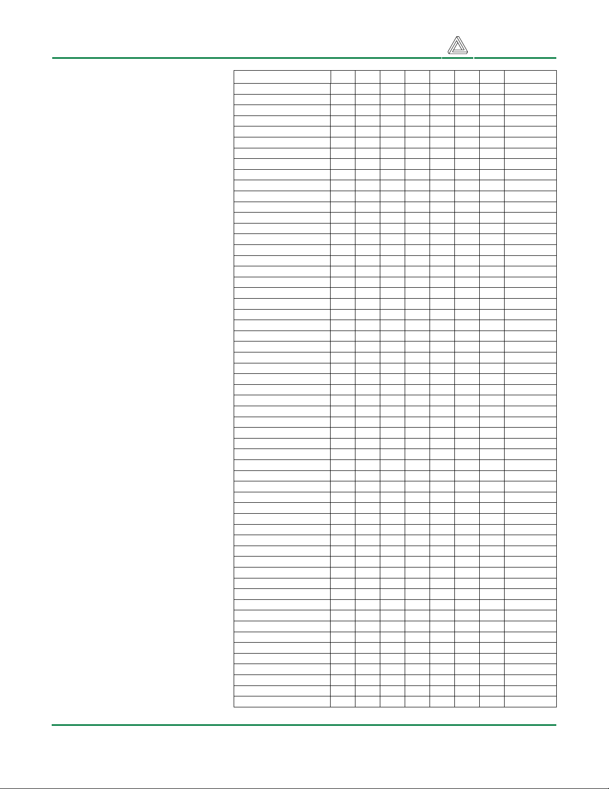
Appendix A: Switch settings
for various synthesizer
frequencies.
Digilent
www.digilentinc.com
Frequency (MHz) M0 M1 M2 M3 M4 N0 N1 VCOSEL
350
337.5
325
312.5
300
287.5
275
262.5
250
237.5
225
212.5
200
187.5
175
168.75
162.5
156.25
150
143.75
137.5
131.25
125
118.75
112.5
106.25
100
93.75
87.5
84.375
81.25
78.125
75
71.875
68.75
65.625
62.5
56.25
53.125
50
46.875
42.1875
40.625
39.0625
37.5
35.9375
34.375
32.8125
31.25
29.6875
28.125
26.5625
25
21.875
20.3125
18.75
17.1875
15.625
0 0 1 1 1 0 0 0
1 1 0 1 1 0 0 0
0 1 0 1 1 0 0 0
1 0 0 1 1 0 0 0
0 0 0 1 1 0 0 0
1 1 1 0 1 0 0 0
0 1 1 0 1 0 0 0
1 0 1 0 1 0 0 0
0 0 1 0 1 0 0 0
1 1 0 0 1 0 0 0
0 1 0 0 1 0 0 0
1 0 0 0 1 0 0 0
0 0 0 0 1 0 0 0
1 1 1 1 0 0 0 0
0 0 1 1 1 1 0 0
1 1 0 1 1 1 0 0
0 1 0 1 1 1 0 0
1 0 0 1 1 1 0 0
0 0 0 1 1 1 0 0
1 1 1 0 1 1 0 0
0 1 1 0 1 1 0 0
1 0 1 0 1 1 0 0
0 0 1 0 1 1 0 0
1 1 0 0 1 1 0 0
0 1 0 0 1 1 0 0
1 0 0 0 1 1 0 0
0 0 0 0 1 1 0 0
1 1 1 1 0 1 0 0
0 0 1 1 1 0 1 0
1 1 0 1 1 0 1 0
0 1 0 1 1 0 1 0
1 0 0 1 1 0 1 0
0 0 0 1 1 0 1 0
1 1 1 0 1 0 1 0
0 1 1 0 1 0 1 0
1 0 1 0 1 0 1 0
0 0 1 0 1 0 1 0
0 1 0 0 1 0 1 0
1 0 0 0 1 0 1 0
0 0 0 0 1 0 1 0
1 1 1 1 0 0 1 0
1 1 0 1 1 1 1 0
0 1 0 1 1 1 1 0
1 0 0 1 1 1 1 0
0 0 0 1 1 1 1 0
1 1 1 0 1 1 1 0
0 1 1 0 1 1 1 0
1 0 1 0 1 1 1 0
0 0 1 0 1 1 1 0
1 1 0 0 1 1 1 0
0 1 0 0 1 1 1 0
1 0 0 0 1 1 1 0
0 0 0 0 1 1 1 0
0 1 1 1 0 1 1 0
1 0 1 1 0 1 1 0
0 0 1 1 0 1 1 0
1 1 0 1 0 1 1 0
0 1 0 1 0 1 1 0
Copyright Digilent, Inc. Page 18/18 Doc: 502-046
 Loading...