

Page 1
EVB-USB3300-XLX User
Manual
The information contained herein is proprietary to SMSC, and shall be used solely in accordance with the agr eement pursuant to which it is provided. Although the information is believed to be accurate, no responsibility is assumed for inaccuracies. SMSC reserves the right to make changes to this document and to specifications and product descriptions at any
time without notice. Neither the provision of this information nor the sale of the de scribed semiconductor devices conveys
any licenses under any patent rights or other intellectual property rights of SMSC or others unless specifically specified
otherwise. The product may contain design defects or erro rs known as anomalies, includi ng but not necessarily limit ed to
any which may be identified in this document, which may cause the product to deviate from published specifications.
SMSC products are not designed, int ended, authorized or warrant ed for use in an y life sup port o r other a pplication wher e
product failure could cause or contribute to personal injury or severe property damage. Any and all such uses without
prior written approval of an officer of SMSC will be fully at the risk of the customer. SMSC is a registered trademark of
Standard Microsystems Corporation (“SMSC”).
SMSC DISCLAIMS AND EXCLUDES ANY AND ALL WARRANTIES, INCLUDING WITHOUT LIMITATION ANY AND
ALL IMPLIED WARRANTIES OF MERCHANTABILITY, FITNESS FOR A PARTICULAR PURPOSE, TITLE, AND
AGAINST INFRINGEMENT AND THE LIKE, AND ANY AND ALL WARRANTIES ARISING FROM ANY COURSE OF
DEALING OR USAGE OF TRADE. IN NO EVENT SHALL SMSC BE LIABLE FOR ANY DIRECT, INCIDENTAL, INDIRECT, SPECIAL, PUNITIVE, OR CONSEQUENTIAL DAMAGES; OR FOR LOST DATA, PROFITS, SAVINGS OR REVENUES OF ANY KIND; REGARDLESS OF THE FORM OF ACTION, WHETHER BASED ON CONTRACT; TORT;
NEGLIGENCE OF SMSC OR OTHERS; STRICT LIABILITY; BREACH OF WARRANTY; OR OTHERWISE; WHETHER
OR NOT ANY REMEDY OF BUYER IS HELD TO HAVE FAILED OF ITS ESSENTIAL PURPOSE, AND WHETHER OR
NOT SMSC HAS BEEN ADVISED OF THE POSSIBILITY OF SUCH DAMAGES.
SMSC EVB-USB3300-XLX Revision 0.4 (06-29-07)
Page 2

1 Introduction
The SMSC USB3300 USB Transceiver features a ULPI interface to support systems implementing a
USB Host, Device, or On-the-Go (OTG) system. SMSC supplies a complete family of PHY products
to meet the needs of many applications.
2 Overview
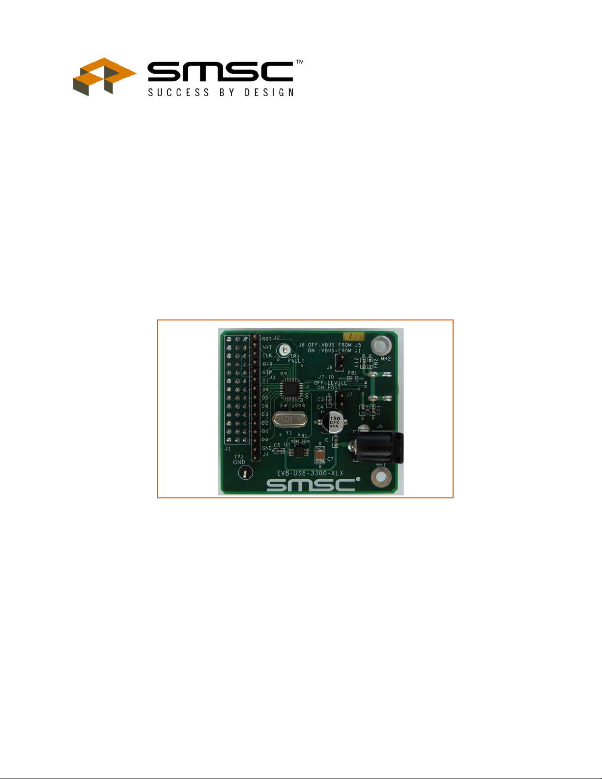
The EVB-USB3300-XLX is a Daughter Card designed to plug into a user's Xil inx ML401 development
system using a header connector. The card attaches to a USB link layer to create a USB Host, Device,
or On-the-Go (OTG) system. The digital interface meets the UTMI+ Low Pin Interface (ULPI)
specification. The ULPI specification can be downloaded from the SMSC web site at
http://www.smsc.com/main/catalog/usb3300.html. The EVB-USB3300-XLX includes the USB300 and
all associated external components. Figure 3 shows a schematic of the EVB.
2.1 3.3 Volt Power Supply
The EVB-USB3300-XLX requires a 3.3 volt supply capable of providing 80mA of current to be present
at the J2 header pins 16, 19, 22 and 25. For device on ly applications this is the only power the EVBUSB3300-XLX requires.
EVB-USB3300-XLX User Manual
2.2 Crystal Oscillator
A 24 MHz crystal is connected to the internal oscillator of the USB3300. A PLL circuit in the USB3300
generates the 60MHz CLKOUT signal used by the link layer.
2.3 USB Connector
A standard Mini-AB connector is provided to attach a USB cable.
2.4 Supplying VBUS Power
In host or OTG applications the EVB-USB3300-XLX must provide 5 volts on V
XLX includes a 5 volt switch that can connect 5 volts to V
can come from either external power supplied at J5 or from header J1 pins 1, 4, 7 and 10. Jumper J6
must be installed to source +5V for the ML501 header. When using J5 to supply external power, J6
must be removed.
The 5 volt switch is controlled by the CPEN signal from the USB3300. The CPEN state is controll ed
by ULPI registers in the USB3300 per the ULPI spec ification. The 5 volt switch has an undervoltage
lockout that turns the switch off if the VBUS voltage is low and the switch prevents reverse current
flow (backdrive) when in the off state. The switch does not provide protection from reverse currents
when in the on state. The user should take care to ensure the switch is off when V
by the USB cable.
In host mode, connector J7 should be installed to add capacitance to V
requires this extra capacitance be present in host implementations.
. The EVB-USB3300-
. The EVB-USB3300-XLX 5 volt supply
BUS
BUS
is being sourced
BUS
. The USB2.0 specification
BUS
Revision 0.4 (06-29-07) SMSC EVB-USB3300-XLX
2
Page 3

EVB-USB3300-XLX User Manual
2.5 Digital I/O
The ULPI signals are routed to connector J1 for connection to the ML401. Each signal on J1 is
described in Table 2.1. All ULPI signals are 3.3V CMOS compatible.
J1 Pin Signal Name J1 Pin Signal Name J1 Pin Signal Name
T able 2.1 Signals on 3x13-Pin Header
1+5V2
4+5V5
7+5V8
10 +5V 11
13 NC 14
16 +3.3V 17
19 +3.3V 20
22 +3.3V 23
25 +3.3V 26
28 NC 29
31 RSVD1 32
34 RSVD2 35
37 RSVD3 38
GND
GND
GND
GND
GND
GND
GND
GND
GND
GND
GND
GND
GND
12
15
18
21
24
27
30
33
36
39
3
6
9
Reset
NXT
CLKOUT
DIR
STP
DATA7
DATA6
DATA5
DATA4
DATA3
DATA2
DATA1
DATA0
SMSC EVB-USB3300-XLX Revision 0.4 (06-29-07)
3
Page 4

2.6 ULPI Signal Test Points
The headers J2, J3 and J4 provide easy access to the ULPI signals, and each pin has a silk screen
label as shown in Figure 1 .
EVB-USB3300-XLX User Manual
Figure 1 ULPI Signal Test Points
2.7 Block Diagram
The EVB-USB3300-XLX block diagram shows how the jumpers are used on the board.
VBUS Switch
500 mA current limit
J5
5V DC
Input
Install to source +5V
from the FPGA
development system.
J1
3x13
Header
5V
VDD3.3
U1
ONA FAULTAn
J6
USB3300
EXTVBUS
CPEN
VDD3.3
ULPI Bus
w/ Fault Detection
5.6uF 150uF
DM
DP
ID
J7
J7 Install for
Host mode
VBUS
DM
DP
ID
GND
USB OTG
Connector
ULPI Signals
24 MHz XTAL
Figure 2 EVB-USB3300-XLX Block Diagram
Revision 0.4 (06-29-07) SMSC EVB-USB3300-XLX
4
Page 5

EVB-USB3300-XLX User Manual
2.8 Schematic Diagram
1
+3.3V
TEST_POINT
Red
TEST_POINT
Red
TP1
2
TP1
C4
150uF
C4
150uF
<Voltage>
10V
<Voltage>
10V
+
+
C3
1.0uF
16VC31.0uF
16V
J7
HDR_1x2J7HDR_1x2
1 2
C7
5.6uF
16VC75.6uF
100K
1/10WR1100K
1/10W
U1
7
9
8
10
GND
OUTB
OUTA
FAULTA
ONA1INA2IN3INB4ONB
6
5
16V
FAULTB
MAX1823BU1MAX1823B
R1
0 = OTG Device
1 = Host
J7
P1
FB1
F-BEAD
500mA / 0.1DCR
FB1
F-BEAD
Keep ferrite beads close
to mini AB connector
500mA / 0.1DCR
Reset
VBUS1D+3D-2ID4GND5SHIELD16SHIELD27SHIELD38SHIELD4
9
MINI-ABP1MINI-AB
FB4
FB4
F-BEAD
F-BEAD
500mA / 0.1DCR
500mA / 0.1DCR
C12
C12
C11
C11
0.1uF
16V
0.1uF
16V
0.1uF
16V
0.1uF
16V
FB2
F-BEAD
FB2
F-BEAD
500mA / 0.1DCR
500mA / 0.1DCR
of
of
of
22Wednesday, November 16, 2005
22Wednesday, November 16, 2005
22Wednesday, November 16, 2005
3930 East Ray Road
Suite 200
Phoenix, Arizona 85044
480-759-0200
3930 East Ray Road
Suite 200
Phoenix, Arizona 85044
480-759-0200
3930 East Ray Road
Suite 200
Phoenix, Arizona 85044
480-759-0200
1
SCH-7065AZ AC
SCH-7065AZ AC
SCH-7065AZ AC
Size Document Number Rev
Date: Sheet
Size Document Number Rev
Date: Sheet
Size Document Number Rev
+3.3V
R6
ZERO
0.1WR6ZERO
0.1W
C10
0.1uF
16V
C10
0.1uF
16V
C9
0.01uF
16VC90.01uF
16V
C8
10uF
6.3VC810uF
6.3V
Date: Sheet
2
EXT_VBUS_DET
C5
1.0uF
16VC51.0uF
16V
3
+5V
J6
0 = External 5V Power Supply
1 = T&MT 5V Power Supply
HDR_1x2J6HDR_1x2
1 2
J4
C1
1.0uF
16VC11.0uF
J5
16V
132
Power_JackJ5Power_Jack
4
5
Circuit Diagrams utilizing SMSC Products Are Included As A Means Of Illustrating
Typical Semiconductor Applications: Consequently Complete Information
Sufficient For Construction Purposes Is Not Necessarily Given. The Information
Has Been Carefully Checked And Is Believed To Be Entirely Reliable. However, No
Responsibility Is Assumed For Inaccuracies. Furthermore, Such Information Does
Not Convey To The Purchaser Of The Semiconductor Devices Described Any
License Under The Patent Rights Of SMSC Or Others. SMSC Reserves The Right
To Make Changes At Any Time In Order To Improve Design And Supply The Best
Product Possible.
D D
C19
10uF
6.3V
C19
10uF
R5
12.0K
1/10WR512.0K
1/10W
9
4
3
VBUS
CPEN
RESET
XI28XO
DATA717DATA618DATA519DATA4
U3
27
C2
33pF
50VC233pF
50V
R41M1/10WR41M
1/10W
Y1
24MhzY124Mhz
C6
33pF
50VC633pF
50V
DATA7
DATA6
DIR
NXT
STP
DATA2
DATA3
DATA4
DATA5
DATA6
DATA7
RESET
CLKOUT
J3
12345
HDR_1x5J3HDR_1x5
J4
12345
12345
J2
HDR_1x5J2HDR_1x5
C C
25
16
8
7
DP
DM
DATA321DATA222DATA1
20
DATA5
DATA4
DATA3
DATA0
DATA1
HDR_1x5J4HDR_1x5
30
31
6
32
5
ID
RBIAS
DATA024NXT11DIR
23
NXT
DATA2
DATA1
DATA0
2
GND1GND
VDD3.3
VDD3.3
VDDA3.3
VDDA3.3
VDDA3.3
USB3300U3USB3300
VDD1.8
VDDA1.8
CLKOUT14STP
VDD1.8
EXT_VBUS_DETECT
12
15
29
13
26
10
C18
4.7uF
6.3V
C18
4.7uF
6.3V
C17
0.1uF
16V
C17
0.1uF
16V
C16
4.7uF
6.3V
C16
4.7uF
6.3V
C15
0.1uF
16V
C15
0.1uF
16V
STP
DIR
EXT_VBUS_DET
CLKOUT
J1J1
+5V
+3.3V
B B
6.3V
TP2
TP2
16V
16V
C20
C20
0.1uF
0.1uF
+3.3VA
16V
16V
C21
C21
0.01uF
0.01uF
FB3
FB3
F-BEAD
F-BEAD
500mA / 0.1DCR
500mA / 0.1DCR
+3.3V
Reset
DIR
STP
CLKOUT
NXT
9
1 342
567
8
11
10 121416
DATA3
DATA4
DATA6
DATA7
DATA5
2730333639
13 15
171819
202122
2324252628293132343537
A A
TEST_POINT
Black
TEST_POINT
Black
DATA2
RSVD1
RSVD2
1
MH
MTG250P125D
MTG250P125D
MH2
MH2
1
MH
MTG250P125D
MTG250P125D
MH1
MH1
3
4
DATA0
DATA1
38
RSVD3
5
Figure 3 EVB-USB3300-XLX Schematic
SMSC EVB-USB3300-XLX Revision 0.4 (06-29-07)
5
Page 6

EVB-USB3300-XLX User Manual
Revision 0.4 (06-29-07) SMSC EVB-USB3300-XLX
6
 Loading...