

Page 1

DDiiggiilleenntt DDIIOO55™™ PPeerriipphheerraall BBooaarrdd
RReeffeerreennccee MMaannuuaal
Revision: August 11, 2005 215 E Main Suite D | Pullman, WA 99163
l
www.digilentinc.com
(509) 334 6306 Voice and Fax
Overview
The DIO5 circuit board provides a ready-made
Connector P2Connector P1
source for many common I/O devices found in
digital systems. It can be connected to Digilent
system boards to create a digital development
platform that is suitable for a wide range of
projects. The DIO5 uses a Xilinx CoolRunner
CPLD to facilitate interaction with system
boards. The CLPD automatically appears in
the JTAG scan chain when the DIO5 is
JTAG
XCR3128XL CoolRunner CPLD
Clock
System Bus
TQ-144
VGA
Port
Uncomitted I/O
attached to a system board, so new designs
can easily be configured into the DIO5. DIO5
features include:
• A Xilinx CoolRunner XCR3128 CPLD for
I/O device and system bus control;
• A 16x2 character LCD module;
• A 4-digit seven segment LED display;
• 16 LEDs in three different colors;
8 switches
16x2
LCD
DIO5 circuit board block diagram
PS2
Port
4 7-seg.
displays
16 LEDs
16 button
keypad
• A 16 button keypad;
• 8 slide switches;
• 3-bit VGA port;
• PS/2 mouse or keyboard port.
The DIO5 has been designed to work
seamlessly with Digilent system boards and all
versions of the Xilinx ISE CAD tools, including
the free WebPack tools available from Xilinx.
The CPLD on the DIO5 is configured during
manufacturing with the project shown in
Appendix 1, but new designs can easily be
loaded into the CPLD.
Functional Description
The Digilab DIO5 can be attached to any
Digilent system board to create a digital design
platform that has many useful I/O devices. The
DIO5 draws power from the system board, so
no separate power supply is required. All I/O
device signals are routed through the on-board
CPLD so that a customized I/O controller can
be created for any given design. For example,
if all on-board I/O devices are needed, a
register-based controller can be implemented.
Or, if only a subset of I/O devices are needed,
a much simpler controller can be used to map
device signals directly through the CPLD to the
system board. Because the CPLD appears in
the JTAG scan chain when the DIO5 is
attached to a system board, it can easily be
configured. The CPLD is programmed during
manufacture with register-based controller
shown in Appendix 1.
Power Supplies
The DIO5 board draws power from three pins
on the 40-pin connectors: pin 37 supplies 3.3V;
pin 39 provides system GND, and pin 40
supplies unregulated voltage (VU). Pin 40 (VU)
is connected directly to an LM1117 5VDC LDO
regulator on the DIO5. 5VDC is used by the
LCD display and the PS/2 interface. The 3.3V
®
Copyright Digilent, Inc. 19 pages Doc: 500-228
Page 2
DIO5 Reference Manual Digilent, Inc.
supply is used to drive the CPLD and all other
I/O devices on the board. During normal
operation, the DIO5 consumes 10-20mA from
the 5V supply, and 50-100mA from the 3.3V
supply depending on how many LEDs are
illuminated. The DIO5 uses a four-layer board,
with two layers dedicated to 3.3V and GND,
and several bulk and high-frequency
decoupling capacitors to keep the supplies
stable under all loads.
CPLD Configuration
The JTAG scan chain is routed through the
DIO5 board on pins 1-4 of connector P1,
allowing the CPLD to be configured from any
Digilent system board. Jumper-shunts must be
loaded on pins 1 & 2 of jumper blocks JP2 and
JP3 on the DIO5 to include the CPLD in the
scan chain, or across pins 2 & 3 to remove the
CPLD from the scan chain.
Jumper position JP1 allows the JTAG signals
on the CPLD to be reclaimed if they are
inadvertently programmed as user I/O’s. Since
the JTAG pins on the CPLD are used only for
programming, this jumper block should not
normally be loaded. The CPLD pinout is
available in appendix 1.
System Board Interface
Signals from all I/O devices on the DIO5 are
routed through the CPLD, with the exception of
the VGA port (video data is too high bandwidth
to pass through the CPLD). All I/O devices on
the DIO5 can therefore be read or written via a
register-based controller in the CPLD. Some
device signals, including the eight slide
switches, the PS/2 data and clock, and an LCD
enable are also routed around the CPLD and
directly to the connectors. These signals can
be accessed either through the CPLD or
directly from the system board.
The CPLD offers several options for moving
data between the DIO5 and a system board: a
memory-mapped bus interface can be defined
where all devices are accessed via registers; a
“direct connect” interface can be defined where
I/O signals pass directly through the CPLD
without the need for a bus (in this case, not all
devices on the DIO5 can be accessed); or
various controllers and compression/encoding
schemes can be used to transfer device data
over subsets of pins.
The default DIO5 CPLD circuit defines a
“system bus” to transfer data to and from a
system board. The bus uses 8 bi-directional
data lines, six address lines, three control
signals, and a clock signal (LCLK). The three
control signals, write enable (WE), output
enable (OE), and chip select (CS), are used to
coordinate bus traffic, and the LCLK signal
provides a clock for latches and controllers on
the DIO5. Four 8-bit write-only registers are
used to receive LED and seven-segment
display data in the CPLD, and three readable
locations contain pushbutton and switch data.
DIO5 Default Circuit Memory Map
Address Read Write
000 BtnLo (buttons 0-7) LedLo (LEDs 0-7)
001 BtnHi (buttons 8-F) LedHi (LEDs 8-F)
010 Swt (slide switches) SsegLo
011 unused SsegHi
10X LCD bus LCD bus
Two read locations, BtnHi and BtnLo, arise
from latches in the CPLD. Pushbutton signals
are stored in these two 8-bit latches at each
rising edge of LCLK. The third read location,
Swt, simply passes switch signals to the
system bus from the switch input pins.
The four writable registers in the CPLD all
provide data to the LED devices (i.e., the
seven-segment displays and discrete LEDs).
The registers use rising-edge-triggered flipflops clocked by the trailing edge of the write
enable signal (WE is active low). Data written
to these registers appears immediately on the
LED’s.
Ten additional pushbutton signals bypass the
system bus, and are routed from the CPLD
directly to pins on the expansion connectors.
Four of these signals contain BCD codes for
buttons 0-9, and six signals are simply the
state of buttons A-F at the output of the
www.digilentinc.com Page 2
Copyright Digilent, Inc. All rights reserved. Other product and company names mentioned may be trademarks of their respective owners.
Page 3
DIO5 Reference Manual Digilent, Inc.
latches. These ten signals are always available
regardless of the system bus state.
The CPLD also contains a seven-segment
display controller. Binary data, in the form of
four 4-bit fields spanning two bytes, can be
written to the seven-segment data registers
and it will be displayed as four hexadecimal
characters on the seven-segment display. The
display controller uses LCLK to control refresh
timing.
Bi-directional LCD data transfers occur over
the system bus. The default CPLD circuit
synthesizes LCD control signals for bus cycles
directed to the LCD memory space, but it is
also possible to drive the LCD control signals
directly. The “LCD” section below provides
information on driving the LCD.
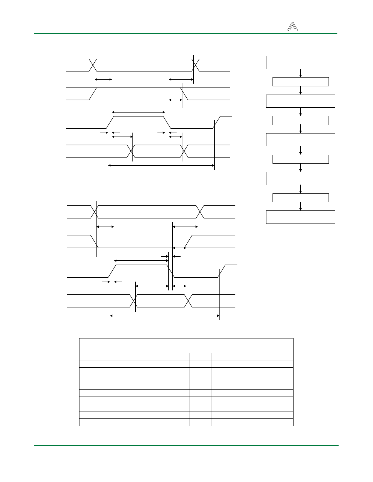
Write Cycle
CS
tdoe
OE
WE
DB0-DB7
Read Cycle
OE
WE
DB0-DB7
System Bus Timing
ten
twd
System bus timings are shown below. Data is
written on the rising edge of write-enable (WE).
DIO5 bus drivers are enabled whenever output
enable (OE) is asserted (low). The diagrams
below show signal timings assumed by Digilent
to create peripheral devices. Different bus and
timing models can be used by modifying
circuits in the FPGA and attached peripheral
devices.
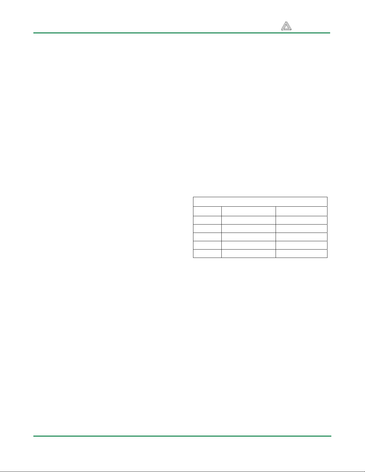
System Bus Timings
Symbol Parameter
ten Time to enable after CS asserted 10ns
th Hold time 1ns
tdoe Disable time after OE deasserted 10ns
teoe Enable time after OE asserted 15ns
tw Write strobe time 10ns
tsu Data setup time 5ns
twd Write disable time 0ns
th
teoe
tw
tsu
th
teoe
tdoe
th
tsu
th
Read data latch time
Time
(typ)
www.digilentinc.com Page 3
Copyright Digilent, Inc. All rights reserved. Other product and company names mentioned may be trademarks of their respective owners.
Page 4
DIO5 Reference Manual Digilent, Inc.
LCD
The DIO5 uses a Powertip 16x2 LCD module
(P/N PC1602ARS-DWA-A) with a Samsung
KS0066U controller (data sheets are available
at the Digilent website).
16 x 2 character LCD
Pin 1
Powertip PC1602ARS
The KS0066U contains a character-generator
ROM (CGROM) with 208 preset 5x8 character
patterns, a character-generator RAM
(CGRAM) that can hold 8 user-defined 5x8
characters, and a display data RAM (DDRAM)
that can hold 80 character codes. Character
codes written into the DDRAM serve as
indexes into the CGROM (or CGRAM). Writing
a character code into a particular DDRAM
location will cause the associated character to
appear at the corresponding display location.
Display positions can be shifted left or right by
setting a bit in the instruction register (IR). The
write-only IR directs display operations (such
as clear display, shift left or right, set DDRAM
address, etc). Available instructions (and the
associated IR codes) are shown in the rightmost column of table 3 below. A busy flag
shows whether the display has competed the
last requested operation; prior to initiating a
new operation, the flag can be checked to see
if the previous operation has been completed.
The display has more DDRAM locations than
can be displayed at any given time. DDRAM
locations 00H to 27H map to the first display
row, and locations 40H to 67H map to the
second row. Normally, DDRAM location 00H
maps to the upper left display corner, and 40H
to the lower left. Shifting the display left or right
can change this mapping. The display uses a
temporary data register (DR) to hold data
during DDRAM /CGRAM reads or writes, and
an internal address register to select the RAM
location. Address register contents, set via the
IR, are automatically incremented after each
read or write operation. The LCD display uses
ASCII character codes. Codes up through 7F
are standard ASCII (which includes all “normal”
alphanumeric characters). Codes above 7F
produce various international characters –
please see the manufacturers data sheet for
more information on international codes.
The display is connected to the DIO5 board by
a 16-pin connector (pins 15 and 16 are for an
optional backlight, and they are not used). The
14-pin interface includes eight data signals,
three control signals, and three voltage supply
signals. The eight data bus signals are passed
through the CPLD to/from the system bus for
read/write cycles directed to the LCD memory
space (address 10X). The three LCD control
signals are driven from the CPLD: the RS
(Register Strobe) signal clocks data into
registers; the R/W signal determines bus
direction; and the E signal enables the bus for
read or write operations. In the standard CPLD
configuration, the R/S and R/W signals are
connected to ADDR0 and WE respectively.
The E signal can be driven directly from the
LCDEN signal available on the system
connector, or if LCDEN is left at logic ‘0’, then
E is driven whenever address “10X” is present
on the bus, CS is asserted, and AS or DS are
low. LCD bus signals and timings are shown
below.
A startup sequence with specific timings
ensures proper LCD operation. After power-on,
at least 20ms must elapse before the functionset instruction code can be written to set the
bus width, number of lines, and character
patterns (8-bit interface, 2 lines, and 5x8 dots
are appropriate). After the function-set
instruction, at least 37us must elapse before
the display-control instruction can be written (to
turn the display on, turn the cursor on or off,
and set the cursor to blink or no blink). After
another 37us, the display-clear instruction can
be issued. After another 1.52ms, the entrymode instruction can set address increment (or
address decrement) mode, and display shift
mode (on or off). After this sequence, data can
be written into the DDRAM to cause
information to appear on the display.
www.digilentinc.com Page 4
Copyright Digilent, Inc. All rights reserved. Other product and company names mentioned may be trademarks of their respective owners.
Page 5
DIO5 Reference Manual Digilent, Inc.
Table 3. LCD Instructions and Codes
Instruction
Clear
Display
Return
Home
Entry mode
set
Display
ON/OFF
control
Cursor or
Display shift
Function Set 0 0 0 0 1 DL N F X X
Set CGRAM
Address
Set DDRAM
address
Read busy
flag/ address
Write data to
RAM
Read data
from RAM
RS R/W DB7 DB6 DB5 DB4 DB3 DB2 DB1 DB0
0 0 0 0 0 0 0 0 0 1
0 0 0 0 0 0 0 0 1 X
0 0 0 0 0 0 0 1 I/D SH
0 0 0 0 0 0 1 D C B
0 0 0 0 0 1 S/C R/L X X
0 0 0 1 AC5 AC4 AC3 AC2 AC1 AC0 Set CGRAM address counter
0 0 1 AC6 AC5 AC4 AC3 AC2 AC1 AC0 Set DDRAM address counter
0 1 BF AC6 AC5 AC4 AC3 AC2 AC1 AC0
1 0 D7 D6 D5 D4 D3 D2 D1 D0
1 1 D7 D6 D5 D4 D3 D2 D1 D0
Instruction bit assignments
Description
Clear display by writing a 20H to
all DDRAM locations; set DDRAM
address register to 00H; and
return cursor to home.
Return cursor to home (upper left
corner), and set DDRAM address
to 0H. DDRAM contents not
changed.
I/D = ‘1’ for right-moving cursor
and address increment; SH = ‘1’
for display shift (direction set by
I/D bit).
Set display (D), cursor (C), and
blinking cursor (B) on or off.
SC = ‘0’ to shift cursor right or left,
‘1’ to shift entire display right or
left (R/L = ‘1’ for right).
Set interface data length (DL = ‘1’
for 8 bit), number of display lines
(N = ‘1’ for 2 lines), display font (F
= ‘0’ for 5x 8 dots)
Read busy flag and address
counter
Write data into DDRAM or
CGRAM, depending on which
address was last set
Read data from DDRAM or
CGRAM, depending on which
address was last set
Table 4. LCD Connector Signals
Pin No. Symbol Signal Description
1 Vss Signal ground
2 Vdd Power supply (5V)
3 Vo Operating (contrast) voltage (LCD drive, typically 100mV at 20C)
4 RS Register select: high for data transfer, low for instruction register
5 R/W Read/write signal: high for read mode, low for write mode
6 E Read/write strobe: high for read OE; falling edge writes data
7-14 Data Bus Bi-directional data bus
www.digilentinc.com Page 5
Copyright Digilent, Inc. All rights reserved. Other product and company names mentioned may be trademarks of their respective owners.
Page 6
DIO5 Reference Manual Digilent, Inc.
LCD Read Cycle
RS
R/W
E
tsu
th
th
tw
tr tf
tD tDH
Power On
Wait for 20ms
Function Set
Wait for 37us
Display Control Set
DB0-DB7
Wait for 37us
Display Clear
Wait for 1.52ms
OK for operati o ns
LCD startup sequence
LCD Write Cycle
RS
R/W
tsu
tw
tc
th
th
tf
E
tr
tsu1 th1
DB0-DB7
tc
Enable cycle time tc 500 ns E
Enable High pulse width tw 220 ns E
Enable rise/fall time tr, tf 25 ns E
RS, R/W setup time tsu 40 ns RS, R/W
RS, R/W hold time th 10 ns RS, R/W
Read data output delay tD 60 120 ns DB0-DB7
Read data hold time tDH 20 ns DB0-DB7
Write data setup time tsu1 40 ns DB0-DB7
Write data hold time th1 10 ns DB0-DB7
Parameter Symbol Min Max Unit Test Pin
www.digilentinc.com Page 6
Copyright Digilent, Inc. All rights reserved. Other product and company names mentioned may be trademarks of their respective owners.
Table 5. LCD Bus Timings
Page 7

DIO5 Reference Manual Digilent, Inc.
Seven-Segment LED display
The DIO5 board contains a modular 4-digit,
common anode seven-segment LED display.
In a common anode display, the seven anodes
of the LEDs forming each digit are connected
to four common circuit nodes (labeled A1
through A4 on the DIO5). Each anode, and
therefore each digit, can be independently
turned on and off by driving these signals to a
‘1’ or a ‘0’. The cathodes of similar segments
on all four displays are also connected
together into seven common circuit nodes
labeled CA through CG. Thus, each cathode
for all four displays can be turned on and off
independently.
This connection scheme creates a multiplexed
display, where driving the anode signals and
corresponding cathode patterns of each digit in
a repeating, continuous succession can create
a 4-digit display. In order for each of the four
digits to appear bright and continuously
illuminated, all four digits should be driven once
every 1 to 16ms (for a refresh frequency of 1KHz
to 60Hz). For example, in a 60Hz refresh
scheme, each digit would be illuminated for ¼ of
the refresh cycle, or 4ms. The controller must
assure that the correct cathode pattern is
present when the corresponding anode signal is
driven. To illustrate the process, if A1 is driven
high while CB and CC are driven low, then a “1”
will be displayed in digit position 2. Then, if A2 is
driven high while CA, CB and CC are driven low,
then a “7” will be displayed in digit position 2. If
A1 and CB, CC are driven for 4ms, and then A2
and CA, CB, CC are driven for 4ms in an
endless succession, the display will show “17” in
the first two digits. An example timing diagram is
provided below.
Common anode
a
A1
A2
A3
b
g
c
d
Refresh period = 1ms to 16ms
afgedcb
Digit period = Refresh / 4
f
e
Seven-segment display detail and cathaode
patterns to display the decimal digits.
Anodes are connected via
transistors for greater current
Vdd
Digit
Shown
0
1
2
3
4
5
6
7
8
9
A2A1
Illuminated Segment
a b c d e f g
1 1 1 1 1 1 0
0 1 1 0 0 0 0
1 1 0 1 1 0 1
1 1 1 1 0 0 1
0 1 1 0 0 1 1
1 0 1 1 0 1 1
1 0 1 1 1 1 1
1 1 1 0 0 0 0
1 1 1 1 1 1 1
1 1 1 1 0 1 1
A3
A4
A4
Cathodes Digit 1 Digit 2 Digit 3 Digit 4
b
a
www.digilentinc.com Page 7
Copyright Digilent, Inc. All rights reserved. Other product and company names mentioned may be trademarks of their respective owners.
Cathodes are connected to
Xilinx device via 100Ω resistors
cdef gdp
Page 8

DIO5 Reference Manual Digilent, Inc.
When configured with the code shown in the
appendix, the CPLD on the DIO5 board
implements a seven-segment controller
provided a suitable clock (256Hz to 1KHz) is
provided on the LCLK pin. The controller
accepts four 4-bit binary numbers in two
successive registers, and decodes and
displays them.
Discrete LEDs
Sixteen individual LEDs (5
Vdd
green, 5 yellow, and 6 red)
are provided for circuit
outputs. The LED cathodes
are driven directly from the
390
CPLD, and the anodes are
tied to Vdd via 390-ohm
resistors (so the LED drive
signals are active low).
When the CPLD is
LD# signal
configured with the code
shown in the appendix, two 8-bit registers (at
writable locations 000 and 001 in the CPLD)
drive the LED cathode signals. Note the LED
signals are inverted in the VHDL code, so a
logic “1” turns on the LEDs.
Pushbutton Inputs
Outputs from the 16 momentary-contact push
buttons are normally low, and are driven high
only while the button is actively pressed. The
buttons exhibit a worst-case bounce time of
about 1ms. A 4.7K series resistor provides
some debounce filtering and ESD protection to
each button. When configured with the code
shown in the appendix, the CPLD on the DIO5
board makes all button signals available on the
bus in two successive readable address
locations (0 and 1).
Vdd
BTN#
signal
4.7KΩ
4.7KΩ
GND
Switch Inputs
The eight slide switches on the DIO5 can be
used to connect either Vdd or GND to eight pins
on the CPLD. The switches exhibit about 2ms of
bounce, and no active debouncing circuit is
employed. A 4.7K-ohm series resistor is used for
nominal input protection. When configured with
the code shown in the appendix, the CPLD
makes all switch signals available on the system
bus at address location 2.
Vdd
SW#
4.7KΩ
GND
signal
PS2 Port
The DIO5 board includes a 6-pin mini-DIN
connector that can accommodate a PS2 mouse
or PS2 keyboard connection. A 5VDC regulator
provides the required voltage to keyboards
and/or mice. Both the mouse and keyboard use
a two-wire serial bus (including clock and data)
to communicate with a host device. These
signals are routed through the CPLD to provide
voltage mapping, and to allow a controller to be
placed in the CPLD.
Pin Definitions
Pin Function
1 Data
2 Reserved
3 GND
4 Vdd
5 Clock
6 Reserved
1
2
4
PS2 Connector
3
6
5
Pin 1
Pin 2
Pin 5Pin 6
Bottom-up
hole pattern
The keyboard and mouse both use identical
signal timings. Both use 11-bit words that include
a start, stop and odd parity bit, but the data
packets are organized differently, and the
keyboard interface allows bi-directional data
transfers (so the host device can illuminate state
LEDs on the keyboard). Bus timings are shown
below. The clock and data signals are only
driven when data transfers occur, and otherwise
they are held in the “idle” state at logic ‘1’. The
timings define signal requirements for mouse-to-
www.digilentinc.com Page 8
Copyright Digilent, Inc. All rights reserved. Other product and company names mentioned may be trademarks of their respective owners.
Page 9

DIO5 Reference Manual Digilent, Inc.
host communications and bi-directional
keyboard communications.
T
T
CK
Edge 0
CLK
DATA
CK
T
T
SU
HLD
'1' stop bit'0' start bit
Edge 10
Symbol Parameter Min Max
T
Clock time
CK
T
Data-to-clock setup time
SU
T
Clock-to-data hold time 5us 25us
HLD
30us
5us
50us
25us
Keyboard
The keyboard uses open collector drivers so
that either the keyboard or an attached host
device can drive the two-wire bus (if the host
device will not send data to the keyboard, then
the host can use simple input-only ports).
PS2-style keyboards use scan codes to
communicate key press data (nearly all
keyboards in use today are PS2 style). Each
key has a single, unique scan code that is sent
whenever the corresponding key is pressed. If
the key is pressed and held, the scan code will
be sent repeatedly once every 100ms or so.
When a key is released, a “F0” key-up code is
sent, followed by the scan code of the released
key. If a key can be “shifted” to produce a new
character (like a capital letter), then a shift
character is sent in addition to the original scan
code, and the host device must determine which
character to use. Some keys, called extended
keys, send an “E0” ahead of the scan code (and
they may send more than one scan code). When
an extended key is released, an “E0 F0” key-up
code is sent, followed by the scan code. Scan
codes for most keys are shown in the figure
below.
A host device can also send data to the
keyboard. Below is a short list of some oftenused commands.
ED Set Num Lock, Caps Lock, and Scroll Lock
LEDs. After receiving an “ED”, the keyboard
returns an “FA”; then the host sends a byte to
set LED status: Bit 0 sets Scroll Lock; bit 1 sets
Num Lock; and Bit 2 sets Caps lock. Bits 3 to 7
are ignored.
EE Echo. Upon receiving an echo command, the
keyboard replies with “EE”.
F3 Set scan code repeat rate. The keyboard
acknowledges receipt of an “F3” by returning an
“FA”, after which the host sends a second byte
to set the repeat rate.
FE Resend. Upon receiving FE, the keyboard re-
sends the last scan code sent.
FF Reset. Resets the keyboard.
ESC
76
` ~
0E
TAB
0D
Caps Lock
58
Shift
12
Ctrl
14
F105F206F304F4
0C
1 !162 @1E3 #264 $255 %
2E
Q
15W1DE24R2DT2C
A
1CS1BD23F2BG34
Z
1ZX22C21V2AB32
Alt
11
F503F60BF783F8
0A
6 ^367 &3D8 *3E9 (460 )45- _4E= +55BackSpace
Y
35U3CI43O44P4D
H
33J3BK42L4B
N
31M3A
Space
29
, <41> .49/ ?
F901F1009F1178F12
07
66
[ {
54
; :
4C
4A
Alt
E0 11
' "
52
] }
5B
\ |
5D
Enter
5A
Shift
59
Ctrl
E0 14
E0 75
E0 74
E0 6B
E0 72
www.digilentinc.com Page 9
Copyright Digilent, Inc. All rights reserved. Other product and company names mentioned may be trademarks of their respective owners.
Page 10

DIO5 Reference Manual Digilent, Inc.
The keyboard should send data to the host
only when both the data and clock lines are
high (or idle). Since the host is the “bus
master”, the keyboard should check to see
whether the host is sending data before driving
the bus. To facilitate this, the clock line can be
used as a “clear to send” signal. If the host
pulls the clock line low, the keyboard must not
send any data until the clock is released (hostto-keyboard data transmission will not be dealt
with further here).
The keyboard sends data to the host in 11-bit
words that contain a ‘0’ start bit, followed by 8bits of scan code (LSB first), followed by an
odd parity bit and terminated with a ‘1’ stop bit.
The keyboard generates 11 clock transitions
(at around 20 - 30KHz) when the data is sent,
and data is valid on the falling edge of the
clock.
Mouse
The mouse outputs a clock and data signal
when it is moved; otherwise, these signals
remain at logic ‘1’. Each time the mouse is
moved, three 11-bit words are sent from the
mouse to the host device. Each of the 11-bit
words contains a ‘0’ start bit, followed by 8 bits of
data (LSB first), followed by an odd parity bit,
and terminated with a ‘1’ stop bit. Thus, each
data transmission contains 33 bits, where bits 0,
11, and 22 are ‘0’ start bits, and bits 11, 21, and
33 are ‘1’ stop bits. The three 8-bit data fields
contain movement data as shown below. Data is
valid at the falling edge of the clock, and the
clock period is 20 to 30KHz.
The mouse assumes a relative coordinate
system wherein moving the mouse to the right
generates a positive number in the X field, and
moving to the left generates a negative number.
Likewise, moving the mouse up generates a
positive number in the Y field, and moving down
represents a negative number (the XS and YS
bits in the status byte are the sign bits – a ‘1’
indicates a negative number). The magnitude of
the X and Y numbers represent the rate of
mouse movement – the larger the number, the
faster the mouse is moving (the XV and YV bits
in the status byte are movement overflow
indicators – a ‘1’ means overflow has occurred).
If the mouse moves continuously, the 33-bit
transmissions are repeated every 50ms or so.
The L and R fields in the status byte indicate Left
and Right button presses (a ‘1’ indicates the
button is being pressed).
Mouse status byte X direction byte Y direction byte
L R 0 1 XS YS XY YY P X0 X1 X2 X3 X4 X5 X6 X7 P Y0 Y1 Y2 Y3 Y4 Y5 Y6 Y7 P10 100 11
Stop bit
Idle state
Idle state
Start bit Stop bit
Start bit
Stop bit
Start bit
VGA Port
VGA "DB15" Connector
The five standard VGA signals Red (R), Green
(G), Blue (B), Horizontal Sync (HS), and
Vertical Sync (VS) are routed directly to the
VGA connector, bypassing the CPLD. A 270ohm series resistor is used on each color
signal. This resistor forms a divider with the 75ohm VGA cable termination, resulting in a
signal that conforms to the VGA specification
(i.e., 0V for fully off and .7V for fully on).
VGA signal timings are specified, published,
copyrighted and sold by the VESA organization
(www.vesa.org). The following VGA system
www.digilentinc.com Page 10
Copyright Digilent, Inc. All rights reserved. Other product and company names mentioned may be trademarks of their respective owners.
1
6
11
2
7
12
3
8
13
4
9
14
5
10
15
GND
270
270
270
R
G
B
HS
VS
Page 11

DIO5 Reference Manual Digilent, Inc.
timing information is provided as an example of
how a VGA monitor might be driven in 640 by
480 mode. For more precise information, or for
information on higher VGA frequencies, refer
to document available at the VESA website (or
experiment!).
VGA system timing
CRT-based VGA displays use amplitude
modulated, moving electron beams (or cathode
rays) to display information on a phosphorcoated screen. LCD displays use an array of
switches that can impose a voltage across a
small amount of liquid crystal, thereby
changing light permitivity through the crystal on
a pixel-by-pixel basis. Although the following
description is limited to CRT displays, LCD
displays have evolved to use the same signal
timings as CRT displays (so the “signals”
discussion below pertains to both CRTs and
LCDs).
CRT displays use electron beams (one for red,
one for blue and one for green) to energize the
phosphor that coats the inner side of the
display end of a cathode ray tube (see drawing
below). Electron beams emanate from
“electron guns”, which are a finely pointed,
heated cathodes placed in close proximity to a
positively charged annular plate called a “grid”.
The electrostatic force imposed by the grid
pulls away rays of energized electrons as current
flows into the cathodes. These particle rays are
initially accelerated towards the grid, but they
soon fall under the influence of the much larger
electrostatic force that results from the entire
phosphor coated display surface of the CRT
being charged to 20kV (or more). The rays are
focused to a fine beam as they pass through the
center of the grids, and then they accelerate to
impact on the phosphor coated display surface.
The phosphor surface glows brightly at the
impact point, and the phosphor continues to glow
for several hundred microseconds after the
beam is removed. The larger the current fed into
the cathode, the brighter the phosphor will glow.
Between the grid and the display surface, the
beam passes through the neck of the CRT
where two coils of wire produce orthogonal
electromagnetic fields. Because cathode rays
are composed of charged particles (electrons),
they can be deflected by these magnetic fields.
Current waveforms are passed through the coils
to produce magnetic fields that interact with the
cathode rays and cause them to transverse the
display surface in a “raster” pattern, horizontally
from left to right and vertically from top to bottom.
As the cathode ray moves over the surface of
the display, the current sent to the electron guns
can be increased or decreased to change the
brightness of the display at the cathode ray
impact point.
Anode (entire screen)
Cathode ray tube
Deflection coils
Cathode ray
Cathode ray tube display system
Grid
Electron guns
(Red, Blue, Green)
R,G,B signals (to guns)
gun
deflection
control
High voltage supply (>20kV)
www.digilentinc.com Page 11
Copyright Digilent, Inc. All rights reserved. Other product and company names mentioned may be trademarks of their respective owners.
grid
control
Control board
control
Sync signals
(to deflection control)
VGA cable
Page 12

DIO5 Reference Manual Digilent, Inc.
Information is only displayed when the beam is
moving in the “forward” direction (left to right
and top to bottom), and not during the time the
beam is reset back to the left or top edge of the
display. Much of the potential display time is
therefore lost in “blanking” periods when the
beam is reset and stabilized to begin a new
horizontal or vertical display pass.
The size of the beams, the frequency at which
the beam can be traced across the display,
and the frequency at which the electron beam
can be modulated determine the display
resolution. Modern VGA displays can
accommodate different resolutions, and a VGA
controller circuit dictates the resolution by
producing timing signals to control the raster
patterns. The controller must produce
synchronizing pulses at 3.3V (or 5V) to set the
frequency at which current flows through the
deflection coils, and it must ensure that video
data is applied to the electron guns at the
correct time. Raster video displays define a
number of “rows” that corresponds to the
number of horizontal passes the cathode makes
over the display area, and a number of
“columns” that corresponds to an area on each
row that is assigned to one “picture element” or
pixel. Typical displays use from 240 to 1200
rows, and from 320 to 1600 columns. The overall
size of a display, and the number of rows and
columns determines the size of each pixel.
Video data typically comes from a video refresh
memory, with one or more bytes assigned to
each pixel location (the DIO5 board uses 3-bits
per pixel). The controller must index into video
memory as the beams move across the display,
and retrieve and apply video data to the display
at precisely the time the electron beam is moving
across a given pixel.
A VGA controller circuit must generate the HS
and VS timings signals and coordinate the
delivery of video data based on the pixel clock.
The pixel clock defines the time available to
display 1 pixel of information. The VS signal
defines the “refresh” frequency of the display, or
Current
through
horizontal
defletion
coil
time
pixel 0,0
640 pixels are displayed each
time the beam travels across
the screen
pixel 0,639
VGA display
surface
pixel 479,0 pixel 479,639
Stable current ramp - information
displayed during this time
Total horizontal time
Horizontal display time
Retrace - no
information
displayed
during this
time
retrace
time
HS
www.digilentinc.com Page 12
Copyright Digilent, Inc. All rights reserved. Other product and company names mentioned may be trademarks of their respective owners.
Horizontal sync signal
sets retrace frequency
"back porch""front porch"
Page 13

DIO5 Reference Manual Digilent, Inc.
the frequency at which all information on the
display is redrawn. The minimum refresh
frequency is a function of the display’s
phosphor and electron beam intensity, with
practical refresh frequencies falling in the 50Hz
to 120Hz range. The number of lines to be
displayed at a given refresh frequency defines
the horizontal “retrace” frequency. For a 640pixel by 480-row display using a 25MHz pixel
clock and 60 +/-1Hz refresh, the signal timings
shown in the table below can be derived.
Timings for sync pulse width and front and
back porch intervals (porch intervals are the
pre- and post-sync pulse times during which
information cannot be displayed) are based on
observations taken from VGA displays.
Symbol Parameter
T
Sync pulse time
S
T
Display time
disp
T
VS pulse width
pw
T
VS front porch
fp
T
VS back porch
bp
Vertical Sync
Time Clocks Lines
16.7ms
15.36ms
320 us
928 us
64 us
416,800
384,000
1,600
8,000
23,200
521
480
2
10
29
A VGA controller circuit decodes the output of a
horizontal-sync counter driven by the pixel clock
to generate HS signal timings. This counter can
be used to locate any pixel location on a given
row. Likewise, the output of a vertical-sync
counter that increments with each HS pulse can
be used to generate VS signal timings, and this
counter can be used to locate any given row.
These two continually running counters can be
used to form an address into video RAM. No
time relationship between the onset of the HS
pulse and the onset of the VS pulse is specified,
so the designer can arrange the counters to
easily form video RAM addresses, or to minimize
decoding logic for sync pulse generation.
Horizontal Sync
Time
32 us
25.6 us
3.84 us
640 ns
1.92 us
Clocks
800
640
96
16
48
T
S
T
disp
T
pw
T
fp
T
bp
XCR3128XL CoolRunner CPLD
The CPLD is in a TQ144 package that has 108
user I/Os available. Of these, 63 are routed to
devices on the DIO5, 17 are assigned to form
a “system bus” that connects the DIO5 and a
system board, 10 connect pushbutton signals
directly to a system board, 6 are uncommitted
I/O signals routed to the system board, and 2
are used to pass PS/2 port signals through to a
system board. The remaining 10 signals are
not connected. CPLD pinouts are shown in the
table below.
The CPLD can contain various controller
circuits to pass DIO5 device signals to an
attached system board. During manufacturing,
the CPLD is configured with the register-based
circuit shown in the Appendix, but the CPLD
can easily be configured with other circuits.
JTAG programming signals are routed across
the expansion connectors from the D2-SB, D2FT, and other system boards, so the CPLD can
be configured whenever the DIO5 is attached to
one of these boards. The CPLD will appear in
the scan chain when shorting blocks are loaded
on pins 1 & 2 of jumpers JP2 & JP3 (conversely,
if shorting blocks are loaded on pins 2 and 3, the
CPLD will not appear in the scan chain). The
center pins of JP2 & JP3 should not be left
floating – jumpers should always be loaded
across pins 1 & 2 or across pins 2 & 3.
Expansion Connectors
The connector pinouts are shown below.
Separately available tables show pass-through
connections for the devices on the DIO5 board
when it is attached to various system boards.
www.digilentinc.com Page 13
Copyright Digilent, Inc. All rights reserved. Other product and company names mentioned may be trademarks of their respective owners.
Page 14

DIO5 Reference Manual Digilent, Inc.
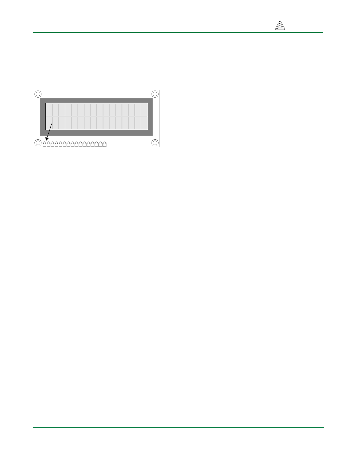
XCR3128XL CPLD Pinout for DIO5 board
Pin # Signal Dir Pin # Signal Dir Pin # Signal Dir Pin # Signal Dir
1 LCDRW out 37 LD7 out 73
2 LCDRS out 38 LD8 out 74 ADR0 in 110 BCOD1 in
3
4
5 IO-02 open 41 LDB out 77 DB0 bidi 113 BOUTA in
6 IO-01 open 42 LDC out 78 ADR1 in 114 BOUTB in
7 KDIN in 43 NC 79 DB1 bidi 115
8 KCIN in 44 LDD out 80 ADR2 in 116 BOUTC in
9 DSPA1 out 45 LDE out 81 DB2 bidi 117 BOUTD in
10 DSPA2 out 46 LDF out 82 ADR3 in 118 BOUTE in
11 DSPA3 out 47 NC 83 DB3 bidi 119 BOUTF in
12 DSPA4 out 48 NC 84 ADR4 in 120 KCLK out
13
14 DSPDP out 50
15 DSPCG out 51
16 DSPCF out 52
17
18 DSPCE out 54 BTN8 in 90 DB6 bidi 126 CLK2 in
19 NC 55 BTN9 in 91 OE in 127 LCLK in
20
21 DSPCD out 57
22 DSPCC out 58
23 DSPCB out 59
24
25 DSPCA out 61 BTN5 in 97 SW6 in 133 IO-05 open
26 LD0 out 62 BTN6 in 98 SW5 in 134 LCDDB0 bidi
27 LD1 out 63 BTND in 99 SW4 in 135
28 LD2 out 64
29 LD3 out 65 BTN1 in 101 SW2 in 137 LCDDB2 bidi
30 LD4 out 66 BTN2 in 102 SW1 in 138 LCDDB3 bidi
31 LD5 out 67 BTN3 in 103 NC 139 LCDDB4 bidi
32 LD6 out 68 BTNE in 104
33
34 NC 70 BTNA in 106 IO-06 open 142 LCDDB7 bidi
35 NC 71 BTNB in 107 LCDEN out 143 LCD-EN out
36 NC 72 BTNF in 108 NC 144
GND
TDI
PORTEN
GND
TMS
VCC33
GND
39 LD9 out 75 NC 111 BCOD2 in
40 LDA out 76
49 NC 85
VCC33
VCC33
GND
53 BTN7 in 89
56 BTNC in 92 DB7 bidi 128 LCLK in
GND
VCC33
GND
60 BTN4 in 96 SW7 in 132 IO-04 open
GND
69 BTN0 in 105
86 DB4 bidi 122 NC
87 ADR5 in 123
88 DB5 bidi 124
93 CS in 129
94 SW8 in 130
95
100 SW3 in 136 LCDDB1 bidi
VCC33
VCC33
GND
TCK
VCC33
TDO
GND
109 BCOD0 in
112 BCOD3 in
121 KDAT out
125 WE in
131 IO-03 open
140 LCDDB5 bidi
141 LCDDB6 bidi
VCC33
VCC33
GND
GND
VCC33
GND
VCC33
www.digilentinc.com Page 14
Copyright Digilent, Inc. All rights reserved. Other product and company names mentioned may be trademarks of their respective owners.
Page 15

DIO5 Reference Manual Digilent, Inc.
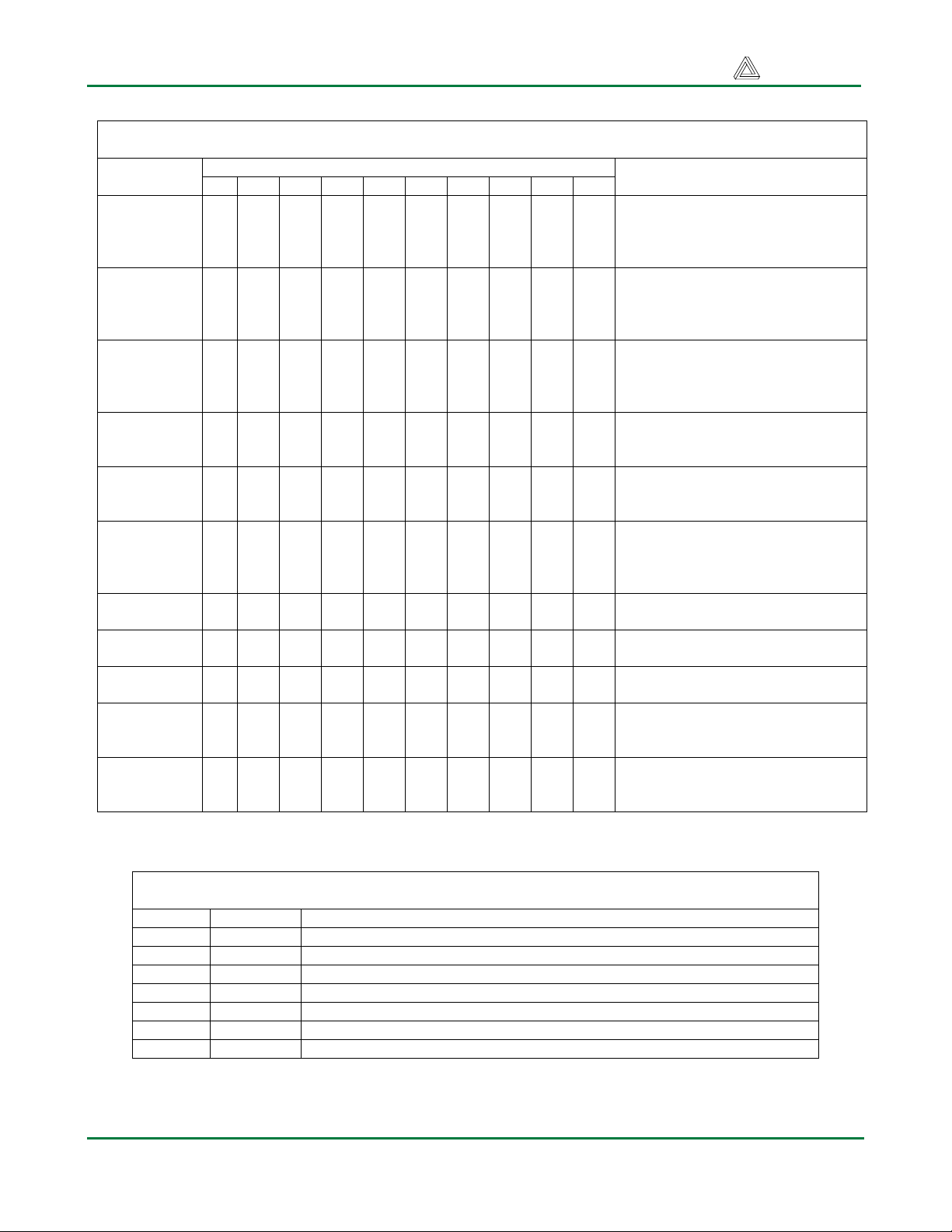
DIO5 Expansion Connector Pinout
P1 Signal Dir P2 Signal Dir
1
2
3
4
5 nc 5 nc
6
7 nc 7 nc
8 nc 8 nc
9 nc 9 nc
10 nc 10 IO-06 open
11 SW1 out 11 CLK2
12 nc 12 IO-05 open
13 SW3 out 13 IO-04 open
14 SW2 out 14 IO-03 open
15 SW5 out 15 IO-02 open
16 SW4 out 16 IO-01 open
17 SW7 out 17 nc
18 SW6 out 18 nc
19 LCLK in 19 KDAT out
20 SW8 out 20 KCLK out
21 DB7 bidi 21 HS in
22 CS in 22 LCLK in
23 DB6 bidi 23 BLU in
24 OE in 24 VS in
25 DB5 bidi 25 RED in
26 WE in 26 GRN in
27 DB4 bidi 27 BOUTE out
28 ADR5 in 28 BOUTF out
29 DB3 bidi 29 BOUTC out
30 ADR4 in 30 BOUTD out
31 DB2 bidi 31 BOUTA out
32 ADR3 in 32 BOUTB out
33 DB1 bidi 33 BCOD2 out
34 ADR2 in 34 BCOD3 out
35 DB0 bidi 35 BCOD0 out
36 ADR1 in 36 BCOD1 out
37
38 ADR0 in 38 LCDEN in
39
40
TDO
TDI
TMS
TCK
JTSEL (VCC33)
VCC33
GND
VU
1 nc
2 nc
3 nc
4 nc
6 nc
37
39
40
VCC33
GND
VU
www.digilentinc.com Page 15
Copyright Digilent, Inc. All rights reserved. Other product and company names mentioned may be trademarks of their respective owners.
Page 16

DIO5 Reference Manual Digilent, Inc.
Appendix 1. Default CPLD configuration
------------------------------------------------------------------------
-- DlabDio5.vhd -- Digilab DIO5 Default CPLD Configuration
------------------------------------------------------------------------
-- Author: Clint Cole
-- Copyright 2003 Digilent, Inc.
------------------------------------------------------------------------
-- This module contains the default configuration for the DIO5 XCR3128XL
-- CoolRunner CPLD. This project implements a bus-oriented, register-based
-- interface that can be used by a system board to interact with the DIO5
-- board. The 16 push buttons, 8 switches, 4 digit seven segment display, and
-- 16 discrete led's are accessed via the CPLD according to the memory map:
-- address read write
-- 000 BtnLo LedLo
-- 001 BtnHi LedHi
-- 010 Swt SsegLo
-- 010 - SsegHi
--
-- The sixteen buttons on the DIO5 are arranged as a decimal keypad and
-- six directly-connected function buttons. All buttons are routed through
-- the CPLD and are readable via the bus interface. Additionally, Buttons 0-9
-- are encoded to BCD by the CPLD logic. The remaining six buttons pass
-- through the CPLD and connect directly to the system board interface
-- connectors. All buttons are debounced by latches driven by the
-- input clock (signal LCLK).
--
-- The eight slide switches bypass the CPLD and connect directly
-- to the interface connectors, and they also pass through the CPLD to allow
-- reading via the bus interface.
--
-- The LCD display signals pass through the CPLD to provide logic level
-- conversion from the 5V logic levels of the LCD display to the 3.3V
-- logic levels used by system boards.
--
-- The VGA signals on the DIO5 board go directly to the connectors and are
-- not connected to the CPLD.
--
-- The keyboard signals pass through the CPLD to provide logic level
-- shifting. The standard implementation provides an input only keyboard
-- and does not support writing to the keyboard.
--
------------------------------------------------------------------------
-- Revision History:
-- 08/20/2003(ClintC): created
------------------------------------------------------------------------
library IEEE;
use IEEE.STD_LOGIC_1164.ALL;
use IEEE.STD_LOGIC_ARITH.ALL;
use IEEE.STD_LOGIC_UNSIGNED.ALL;
entity DlabDio5 is
Port ( db : inout std_logic_vector(7 downto 0);
adr : in std_logic_vector(5 downto 0);
lclk : in std_logic;
cs : in std_logic;
we : in std_logic;
oe : in std_logic;
lcen : in std_logic;
rgbLcd : inout std_logic_vector(7 downto 0);
lcden : out std_logic;
lcdrw : out std_logic;
lcdrs : out std_logic;
rgbBtnIn : in std_logic_vector(15 downto 0);
www.digilentinc.com Page 16
Copyright Digilent, Inc. All rights reserved. Other product and company names mentioned may be trademarks of their respective owners.
Page 17

DIO5 Reference Manual Digilent, Inc.
rgbSwt : in std_logic_vector(7 downto 0);
encBtn : out std_logic_vector(3 downto 0);
rgbBtnOt : out std_logic_vector(5 downto 0);
rgbLed : out std_logic_vector(15 downto 0);
rgbSsgAn : out std_logic_vector(3 downto 0);
rgbSsgCa : out std_logic_vector(7 downto 0);
kclk : out std_logic;
kdat : out std_logic;
kcin : in std_logic;
kdin : in std_logic);
end DlabDio5;
architecture Behavioral of DlabDio5 is
------------------------------------------------------------------------
-- Component Declarations
------------------------------------------------------------------------
------------------------------------------------------------------------
-- Constant and Signal Declarations
------------------------------------------------------------------------
-- Internal registers for output devices
signal regLed : std_logic_vector(15 downto 0);
signal regSsg : std_logic_vector(15 downto 0);
signal regBtn : std_logic_vector(15 downto 0);
signal rgbSyncBtn : std_logic_vector(15 downto 0);
-- Other needed signals
signal busDout : std_logic_vector(7 downto 0);
signal cntDig : std_logic_vector(1 downto 0) := "00";
signal ssg : std_logic_vector(6 downto 0);
signal dig : std_logic_vector(3 downto 0);
signal an : std_logic_vector(3 downto 0);
----------------------------------------------------------------------------
-- Module Implementation
----------------------------------------------------------------------------
begin
------------------------------------------------------------------------
-- Bus drive control logic. Data bus is driven only when oe and cs are valid.
------------------------------------------------------------------------
db <= busDout when (oe = '0' and cs = '0') else "ZZZZZZZZ";
-- Output mux to place selected data on bus
busDout <= rgbSyncBtn(7 downto 0) when adr = "000000" else
rgbSyncBtn(15 downto 8) when adr = "000001" else
rgbSwt when adr = "000010" else
rgbLcd;
------------------------------------------------------------------------
-- Registers for On-Board Output Devices (LEDs and Sseg display)
------------------------------------------------------------------------
-- The WE signal is driven from a global clock buffer.
process (we)
begin
if (we'event and we = '1') then
if (adr = "000000" and cs = '0') then regLed( 7 downto 0) <= db; end if;
if (adr = "000001" and cs = '0') then regLed(15 downto 8) <= db; end if;
if (adr = "000010" and cs = '0') then regSsg( 7 downto 0) <= db; end if;
www.digilentinc.com Page 17
Copyright Digilent, Inc. All rights reserved. Other product and company names mentioned may be trademarks of their respective owners.
Page 18

DIO5 Reference Manual Digilent, Inc.
if (adr = "000011" and cs = '0') then regSsg(15 downto 8) <= db; end if;
end if;
end process;
-- Assign outputs of the LED holding registers to the led outputs
rgbLed <= not regLed;
------------------------------------------------------------------------
-- Synthesize control signals for the LCD display
------------------------------------------------------------------------
rgbLcd <= db when (cs = '0' and we = '0') else "ZZZZZZZZ";
lcden <= '1' when (adr = "0001--" and cs = '0' and not ((we = '1') and (oe = '1'))) or
lcen = '1' else '0';
lcdrw <= we;
lcdrs <= adr(0);
------------------------------------------------------------------------
-- Get button inupts: All 16 button inputs are registered. Six buttons
-- (A through F) are passed directly through to output pins on the CPLD,
-- and ten buttons (0 through 9) are encoded to BCD.
------------------------------------------------------------------------
-- Register all buttons
process(rgbBtnIn, lclk)
begin
if lclk = '1' and lclk'Event
then regBtn <= rgbBtnIn;
end if;
end process;
rgbSyncBtn <= regBtn;
-- Assign debounced pass-through buttons to their outputs
rgbBtnOt <= rgbSyncBtn(15 downto 10);
-- 10-4 Line BCD Encoder for Buttons
encBtn <= "0000" when rgbSyncBtn(0) = '1' else
"0001" when rgbSyncBtn(1) = '1' else
"0010" when rgbSyncBtn(2) = '1' else
"0011" when rgbSyncBtn(3) = '1' else
"0100" when rgbSyncBtn(4) = '1' else
"0101" when rgbSyncBtn(5) = '1' else
"0110" when rgbSyncBtn(6) = '1' else
"0111" when rgbSyncBtn(7) = '1' else
"1000" when rgbSyncBtn(8) = '1' else
"1001" when rgbSyncBtn(9) = '1' else
"1111";
------------------------------------------------------------------------
-- Seven Segment Display Driver
------------------------------------------------------------------------
-- Counter to cycle around the four digit numbers.
process (lclk)
begin
if lclk = '1' and lclk'Event then
cntDig <= cntDig + 1;
end if;
end process;
-- Seven Segment Display Decoder. This logic defines a four bit binary to
-- seven segment decoder. The output produces a logic 1 for each segment
-- that should be on and a logic 0 for each segment that should be off.
-- Segment A is the least significant bit.
www.digilentinc.com Page 18
Copyright Digilent, Inc. All rights reserved. Other product and company names mentioned may be trademarks of their respective owners.
Page 19

DIO5 Reference Manual Digilent, Inc.
ssg <= "0111111" when dig = "0000" else
"0000110" when dig = "0001" else
"1011011" when dig = "0010" else
"1001111" when dig = "0011" else
"1100110" when dig = "0100" else
"1101101" when dig = "0101" else
"1111101" when dig = "0110" else
"0000111" when dig = "0111" else
"1111111" when dig = "1000" else
"1101111" when dig = "1001" else
"1110111" when dig = "1010" else
"1111100" when dig = "1011" else
"0111001" when dig = "1100" else
"1011110" when dig = "1101" else
"1111001" when dig = "1110" else
"1110001" when dig = "1111" else
"0000000";
-- Digit multiplexor. The anode for each digit in enabled
-- in succession, and the appropriate cathode data is muxed onto
-- the cathode lines while the corresponding anode is driven.
an <= "1110" when cntDig = "00" else
"1101" when cntDig = "01" else
"1011" when cntDig = "10" else
"0111" when cntDig = "11" else
"1111";
dig <= regSsg(15 downto 12) when cntDig = "00" else
regSsg(11 downto 8) when cntDig = "01" else
regSsg( 7 downto 4) when cntDig = "10" else
regSsg( 3 downto 0);
-- Map the internal signals to the pins on the CPLD.
rgbSsgAn <= an;
rgbSsgCa <= '1' & (not ssg);
kclk <= kcin;
kdat <= kdin;
end Behavioral;
www.digilentinc.com Page 19
Copyright Digilent, Inc. All rights reserved. Other product and company names mentioned may be trademarks of their respective owners.
 Loading...