

Page 1

DDiiggiilleenntt DDIIOO44™™ PPeerriipphheerraall BBooaarrdd
RReeffeerreennccee MMaannuuaal
Revision: August 11, 2004 215 E Main Suite D | Pullman, WA 99163
l
www.digilentinc.com
(509) 334 6306 Voice and Fax
Overview
The DIO4 circuit board provides a low-cost,
ready-made source for many of the most
common I/O devices found in digital systems. It
can be attached to a Digilent system board to
create a circuit design platform capable of
hosting a wide array of circuits. DIO4 features
include:
• A 4-digit seven segment LED display;
• 8 individual LEDs;
• 4 pushbuttons;
• 8 slide switches;
• 3-bit VGA port;
• PS/2 mouse or keyboard port.
Functional Description
The DIO4 can be attached to Digilent system
boards to quickly and easily add several useful
I/O devices. The DIO4 draws power from the
system board, and signals from all I/O devices
are routed to individual pins on the system
board connectors. These features allow the
DIO4 to be incorporated into system-board
circuits with minimal effort.
All devices on the DIO4 use the 3.3V supply
from the system board, except for the PS/2
port which needs a 5VDC supply (the DIO4
contains a 5VDC regulator). Signals coming
from the PS/2 port are routed through levelshifting buffers to protect system boards that
do not have 5V tolerant inputs.
Power Supplies
The DIO4 draws power from three pins on the
40-pin connectors: pin 37 supplies 3.3V; pin 39
Connector P2Connector P1
Latch Debounce Buffer
VGA
8 LEDs
4 7-seg.
displays
4 buttons
Port
PS2
Port
8 switches
DIO4 circuit board block diagram
provides system GND, and pin 40 supplies
unregulated voltage (VU). VU is connected to a
5VDC LDO regulator to produce a 5VDC supply
for the PS/2 interface. The 3.3V supply is used to
drive all other I/O devices on the board. The
DIO4 consumes 5-10mA from the VU supply,
and 10-50mA from the 3.3V supply (depending
on how many LEDs are illuminated).
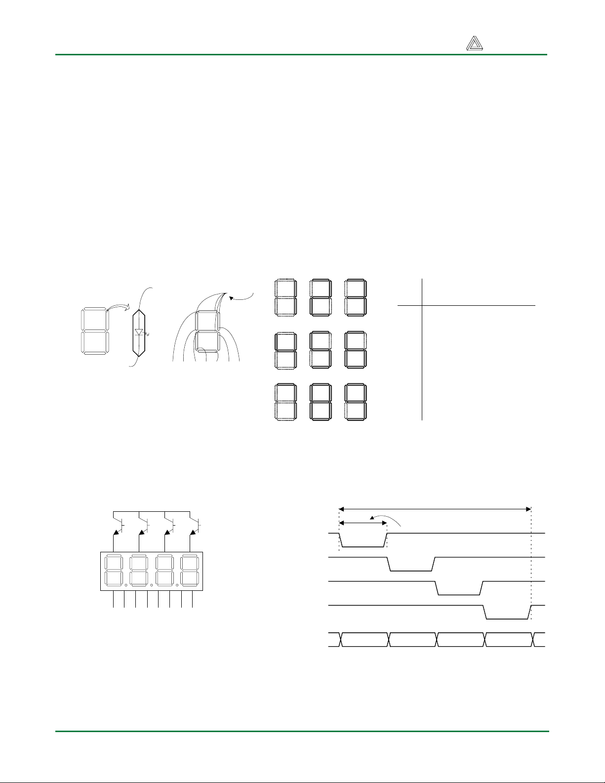
Seven-Segment LED display
The DIO4 board contains a modular 4-digit,
common anode seven-segment LED display. In
a common anode display, the seven anodes of
the LEDs forming each digit are connected to
four common circuit nodes (labeled AN1 through
AN4 on the DIO4). Each anode, and therefore
each digit, can be independently turned on and
off by driving these signals to a ‘0’ (on) or a ‘1’
(off). The cathodes of similar segments on all
four displays are also connected together into
seven common circuit nodes labeled CA through
CG. Thus, each cathode for all four displays can
be turned on (‘0’) and off (‘1’) independently.
®
Doc: 500-227 page 1 of 9
Copyright Digilent, Inc. All rights reserved. Other product and company names mentioned may be trademarks of their respective owners.
Page 2
DIO4 Reference Manual Digilent, Inc.
This connection scheme creates a multiplexed
display, where driving the anode signals and
corresponding cathode patterns of each digit in
a repeating, continuous succession can create
a 4-digit display. In order for each of the four
digits to appear bright and continuously
illuminated, all four digits should be driven
once every 1 to 16ms (for a refresh frequency
of 1KHz to 60Hz). For example, in a 60Hz
refresh scheme, each digit would be
illuminated for ¼ of the refresh cycle, or 4ms.
The controller must assure that the correct
cathode pattern is present when the
Common anode
a
f
e
Figure 4. (a) Seven segment display detail.
(b) common anode display configuration. (c)
segement illumination patterns for decimal
digits. (d) segment illumination tr uth table.
b
g
c
d
(a) (b)
afgedcb
corresponding anode signal is driven. To
illustrate the process, if AN1 is driven low while
CB and CC are driven low, then a “1” will be
displayed in digit position 1. Then, if AN2 is
driven low while CA, CB and CC are driven low,
then a “7” will be displayed in digit position 2. If
AN1 and CB, CC are driven for 4ms, and then
AN2 and CA, CB, CC are driven for 4ms in an
endless succession, the display will show “17” in
the first two digits. An example timing diagram is
provided below.
Digit
Shown
0
1
2
3
4
5
6
7
8
9
(c)
Illuminated Segment
a b c d e f g
1 1 1 1 1 1 0
0 1 1 0 0 0 0
1 1 0 1 1 0 1
1 1 1 1 0 0 1
0 1 1 0 0 1 1
1 0 1 1 0 1 1
1 0 1 1 1 1 1
1 1 1 0 0 0 0
1 1 1 1 1 1 1
1 1 1 1 0 1 1
(d)
Anodes -- connected to CPLD
via transistors for greater current
Vdd
AN3
AN4
AN2AN1
Refresh period = 1ms to 16ms
Digit period = Refres h / 4
AN1
AN2
AN3
abcdefgdp
Cathodes -- connected to
CPLD pins via 100Ω resistor
AN4
Cathodes
Digit 1 Digit 2 Digit 3 Digit 4
www.digilentinc.com Page 2
Page 3

DIO4 Reference Manual Digilent, Inc.
Discrete LEDs
Eight individual LEDs are provided for circuit
outputs. The LED cathodes are tied to GND via
270-ohm resistors, and the LED anodes are
driven from a 74HC373. The ‘373 allows LED
data to be latched on the DIO4, so that the
LD# signals from the system board do not
need to be driven continuously (the LD#
signals use connector pins that are used in the
“system bus” on some Digilent boards). If the
system bus is not needed, then the LDG signal
can be tied high.
74HC373
LD #
LDG
4.7K
4.7K
GND
DQ
G
270
Ohm
GNDGND
Button Inputs
The DIO4 contains 4 N.O. (normally open)
pushbuttons. Button outputs are connected to
Vdd via a 4.7K resistor. When the button is
pressed, the output is connected directly to
GND. This results in a logic signal that is low
only while the button is actively pressed, and
high at all other times. The buttons are
debounced with an RC filter and Schmidttrigger inverter as shown in the figure below.
This circuit creates a logic high signal when the
button is pressed. The debounce circuit
provides ESD protection and creates a signal
with clean edges, so the BTN# signals can be
used as clock signals if desired.
Vdd
4.7K
BTN#
4.7K
.1uF
Switch Inputs
The eight slide switches on the DIO4 can be
used to generate logic high or logic low inputs to
the attached system board. The switches exhibit
about 2ms of bounce, and no active debouncing
circuit is employed. A 4.7K-ohm series resistor is
used for nominal input protection.
Vdd
SW#
4.7KΩ
GND
signal
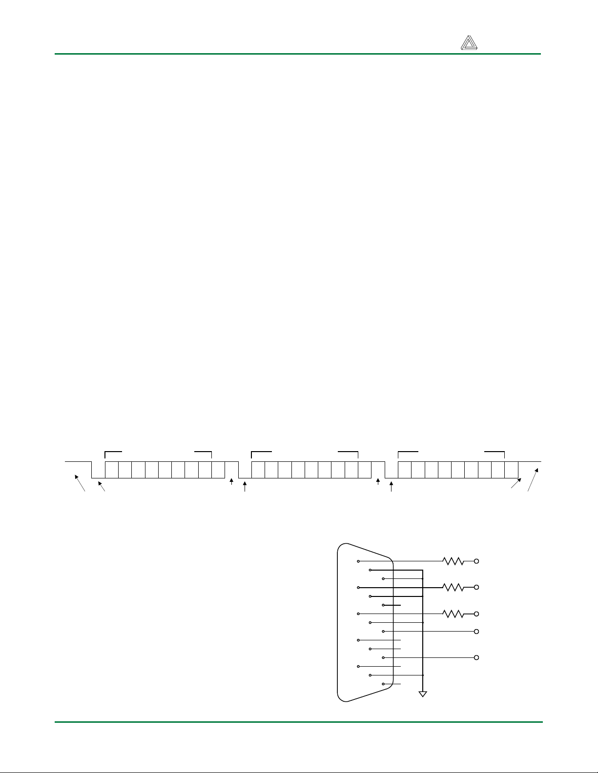
PS2 Port
The DIO4 board includes a 6-pin mini-DIN
connector that can accommodate a PS2 mouse
or PS2 keyboard connection. A 5VDC regulator
and voltage-mapping buffers are provided on the
board to interface lower voltage system boards
with keyboards and/or mice.
Pin 1
Pin 2
1
2
4
PS2 Connector
3
6
5
Pin 5Pin 6
Bottom-up
hole pattern
Both the mouse and keyboard use a two-wire
serial bus (including clock and data) to
communicate with a host device, and both drive
the bus with identical signal timings. Both use
11-bit words that include a start, stop and odd
parity bit, but the data packets are organized
differently, and the keyboard interface allows bidirectional data transfers (so the host device can
illuminate state LEDs on the keyboard). Bus
timings are shown below. The clock and data
signals are only driven when data transfers
occur, and otherwise they are held in the “idle”
state at logic ‘1’. The timings define signal
requirements for mouse-to-host communications
and bi-directional keyboard communications.
Pin Definitions
Pin Function
1 Data
2 Reserved
3 GND
4 Vdd
5 Clock
6 Reserved
www.digilentinc.com Page 3
Page 4
DIO4 Reference Manual Digilent, Inc.
T
T
CK
Edge 0
CLK
DATA
CK
T
T
SU
HLD
'1' stop bit'0' start bit
Edge 10
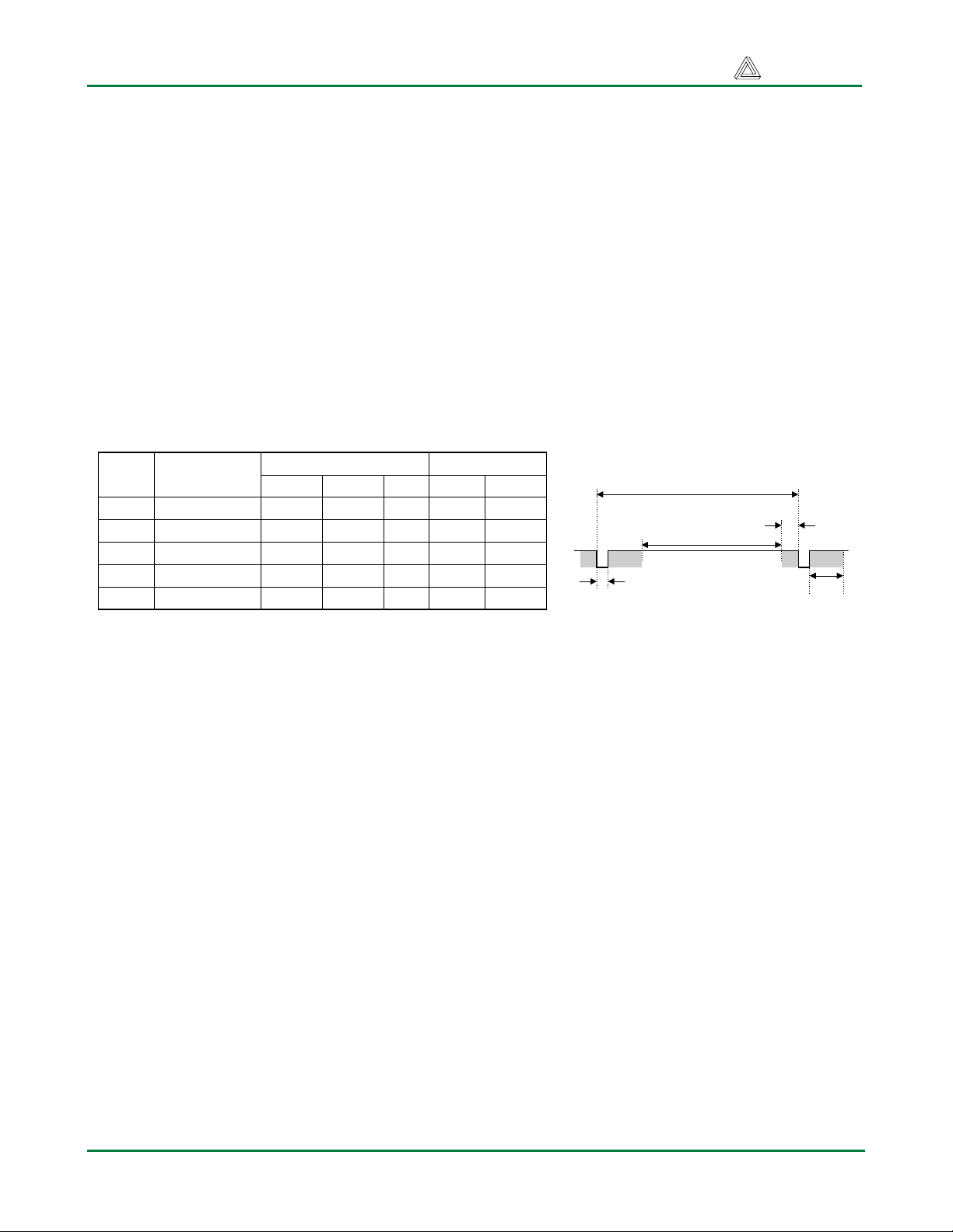
Symbol Parameter Min Max
T
Clock time
CK
T
Data-to-clock setup time
SU
T
Clock-to-data hold time 5us 25us
HLD
30us
5us
50us
25us
Keyboard
The keyboard uses open collector drivers so
that either the keyboard or an attached host
device can drive the two-wire bus (if the host
device will not send data to the keyboard, then
the host can use simple input-only ports).
PS2-style keyboards use scan codes to
communicate key press data (nearly all
keyboards in use today are PS2 style). Each
key has a single, unique scan code that is sent
whenever the corresponding key is pressed. If
the key is pressed and held, the scan code will
be sent repeatedly once every 100ms or so.
When a key is released, a “F0” key-up code is
sent, followed by the scan code of the released
key. If a key can be “shifted” to produce a new
character (like a capital letter), then a shift
character is sent in addition to the original scan
code, and the host device must determine which
character to use. Some keys, called extended
keys, send an “E0” ahead of the scan code (and
they may send more than one scan code). When
an extended key is released, an “E0 F0” key-up
code is sent, followed by the scan code. Scan
codes for most keys are shown in the figure
below.
A host device can also send data to the
keyboard. Below is a short list of some oftenused commands.
ED Set Num Lock, Caps Lock, and Scroll Lock
LEDs. After receiving an “ED”, the keyboard
returns an “FA”; then the host sends a byte to
set LED status: Bit 0 sets Scroll Lock; bit 1 sets
Num Lock; and Bit 2 sets Caps lock. Bits 3 to 7
are ignored.
EE Echo. Upon receiving an echo command, the
keyboard replies with “EE”.
F3 Set scan code repeat rate. The keyboard
acknowledges receipt of an “F3” by returning an
“FA”, after which the host sends a second byte
to set the repeat rate.
FE Resend. Upon receiving FE, the keyboard re-
sends the last scan code sent.
FF Reset. Resets the keyboard.
ESC
76
` ~
0E
TAB
0D
Caps Lock
58
Shift
12
Ctrl
14
F105F206F304F4
0C
1 !162 @1E3 #264 $255 %
2E
Q
15W1DE24R2DT2C
A
1CS1BD23F2BG34
Z
1ZX22C21V2AB32
Alt
11
F503F60BF783F8
0A
6 ^367 &3D8 *3E9 (460 )45- _4E= +55BackSpace
Y
35U3CI43O44P4D
H
33J3BK42L4B
N
31M3A
Space
29
, <41> .49/ ?
F901F1009F1178F12
07
66
[ {
54
; :
4C
4A
Alt
E0 11
' "
52
] }
5B
\ |
5D
Enter
5A
Shift
59
Ctrl
E0 14
E0 75
E0 74
E0 6B
E0 72
www.digilentinc.com Page 4
Page 5
DIO4 Reference Manual Digilent, Inc.
The keyboard should send data to the host
only when both the data and clock lines are
high (or idle). Since the host is the “bus
master”, the keyboard should check to see
whether the host is sending data before driving
the bus. To facilitate this, the clock line can be
used as a “clear to send” signal. If the host
pulls the clock line low, the keyboard must not
send any data until the clock is released (hostto-keyboard data transmission will not be dealt
with further here).
The keyboard sends data to the host in 11-bit
words that contain a ‘0’ start bit, followed by 8bits of scan code (LSB first), followed by an
odd parity bit and terminated with a ‘1’ stop bit.
The keyboard generates 11 clock transitions
(at around 20 - 30KHz) when the data is sent,
and data is valid on the falling edge of the
clock.
Mouse
The mouse outputs a clock and data signal
when it is moved; otherwise, these signals
remain at logic ‘1’. Each time the mouse is
moved, three 11-bit words are sent from the
mouse to the host device. Each of the 11-bit
words contains a ‘0’ start bit, followed by 8 bits of
data (LSB first), followed by an odd parity bit,
and terminated with a ‘1’ stop bit. Thus, each
data transmission contains 33 bits, where bits 0,
11, and 22 are ‘0’ start bits, and bits 11, 21, and
33 are ‘1’ stop bits. The three 8-bit data fields
contain movement data as shown below. Data is
valid at the falling edge of the clock, and the
clock period is 20 to 30KHz.
The mouse assumes a relative coordinate
system wherein moving the mouse to the right
generates a positive number in the X field, and
moving to the left generates a negative number.
Likewise, moving the mouse up generates a
positive number in the Y field, and moving down
represents a negative number (the XS and YS
bits in the status byte are the sign bits – a ‘1’
indicates a negative number). The magnitude of
the X and Y numbers represent the rate of
mouse movement – the larger the number, the
faster the mouse is moving (the XV and YV bits
in the status byte are movement overflow
indicators – a ‘1’ means overflow has occurred).
If the mouse moves continuously, the 33-bit
transmissions are repeated every 50ms or so.
The L and R fields in the status byte indicate Left
and Right button presses (a ‘1’ indicates the
button is being pressed).
Mouse status byte X direction byte Y direction byte
L R 0 1 XS YS XY YY P X0 X1 X2 X3 X4 X5 X6 X7 P Y0 Y1 Y2 Y3 Y4 Y5 Y6 Y7 P10 100 11
Idle state
Start bit Stop bit
Start bit
VGA Port
The five standard VGA signals Red (R), Green
(G), Blue (B), Horizontal Sync (HS), and
Vertical Sync (VS) are routed directly to the
VGA connector. A 270-ohm series resistor is
used on each color signal. This resistor forms
a divider with the 75-ohm VGA cable
termination, resulting in a signal that conforms
to the VGA specification (i.e., 0V for fully off
and .7V for fully on).
VGA signal timings are specified, published,
copyrighted and sold by the VESA organization
(www.vesa.org). The following VGA system
Stop bit
1
6
2
7
3
8
4
9
5
Start bit
VGA "DB15" Connector
270
11
270
12
270
13
14
10
15
GND
Stop bit
Idle state
R
G
B
HS
VS
www.digilentinc.com Page 5
Page 6

DIO4 Reference Manual Digilent, Inc.
timing information is provided as an example of
how a VGA monitor might be driven in 640 by
480 mode. For more precise information, or for
information on higher VGA frequencies, refer
to document available at the VESA website (or
experiment!).
VGA system timing
CRT-based VGA displays use amplitude
modulated, moving electron beams (or cathode
rays) to display information on a phosphorcoated screen. LCD displays use an array of
switches that can impose a voltage across a
small amount of liquid crystal, thereby
changing light permitivity through the crystal on
a pixel-by-pixel basis. Although the following
description is limited to CRT displays, LCD
displays have evolved to use the same signal
timings as CRT displays (so the “signals”
discussion below pertains to both CRTs and
LCDs).
CRT displays use electron beams (one for red,
one for blue and one for green) to energize the
phosphor that coats the inner side of the
display end of a cathode ray tube (see drawing
below). Electron beams emanate from
“electron guns”, which are a finely pointed,
heated cathodes placed in close proximity to a
positively charged annular plate called a “grid”.
The electrostatic force imposed by the grid
pulls away rays of energized electrons as current
flows into the cathodes. These particle rays are
initially accelerated towards the grid, but they
soon fall under the influence of the much larger
electrostatic force that results from the entire
phosphor coated display surface of the CRT
being charged to 20kV (or more). The rays are
focused to a fine beam as they pass through the
center of the grids, and then they accelerate to
impact on the phosphor coated display surface.
The phosphor surface glows brightly at the
impact point, and the phosphor continues to glow
for several hundred microseconds after the
beam is removed. The larger the current fed into
the cathode, the brighter the phosphor will glow.
Between the grid and the display surface, the
beam passes through the neck of the CRT
where two coils of wire produce orthogonal
electromagnetic fields. Because cathode rays
are composed of charged particles (electrons),
they can be deflected by these magnetic fields.
Current waveforms are passed through the coils
to produce magnetic fields that interact with the
cathode rays and cause them to transverse the
display surface in a “raster” pattern, horizontally
from left to right and vertically from top to bottom.
As the cathode ray moves over the surface of
the display, the current sent to the electron guns
can be increased or decreased to change the
brightness of the display at the cathode ray
impact point.
Anode (entire screen)
Cathode ray tube
Deflection coils
Cathode ray
Cathode ray tube display system
Grid
Electron guns
(Red, Blue, Green)
R,G,B signals (to guns)
gun
deflection
control
High voltage supply (>20kV)
www.digilentinc.com Page 6
grid
control
Control board
control
Sync signals
(to deflection control)
VGA cable
Page 7
DIO4 Reference Manual Digilent, Inc.
Information is only displayed when the beam is
moving in the “forward” direction (left to right
and top to bottom), and not during the time the
beam is reset back to the left or top edge of the
display. Much of the potential display time is
therefore lost in “blanking” periods when the
beam is reset and stabilized to begin a new
horizontal or vertical display pass.
The size of the beams, the frequency at which
the beam can be traced across the display,
and the frequency at which the electron beam
can be modulated determine the display
resolution. Modern VGA displays can
accommodate different resolutions, and a VGA
controller circuit dictates the resolution by
producing timing signals to control the raster
patterns. The controller must produce
synchronizing pulses at 3.3V (or 5V) to set the
frequency at which current flows through the
deflection coils, and it must ensure that video
data is applied to the electron guns at the
correct time. Raster video displays define a
number of “rows” that corresponds to the
number of horizontal passes the cathode makes
over the display area, and a number of
“columns” that corresponds to an area on each
row that is assigned to one “picture element” or
pixel. Typical displays use from 240 to 1200
rows, and from 320 to 1600 columns. The overall
size of a display, and the number of rows and
columns determines the size of each pixel.
Video data typically comes from a video refresh
memory, with one or more bytes assigned to
each pixel location (the DIO4 board uses 3-bits
per pixel). The controller must index into video
memory as the beams move across the display,
and retrieve and apply video data to the display
at precisely the time the electron beam is moving
across a given pixel.
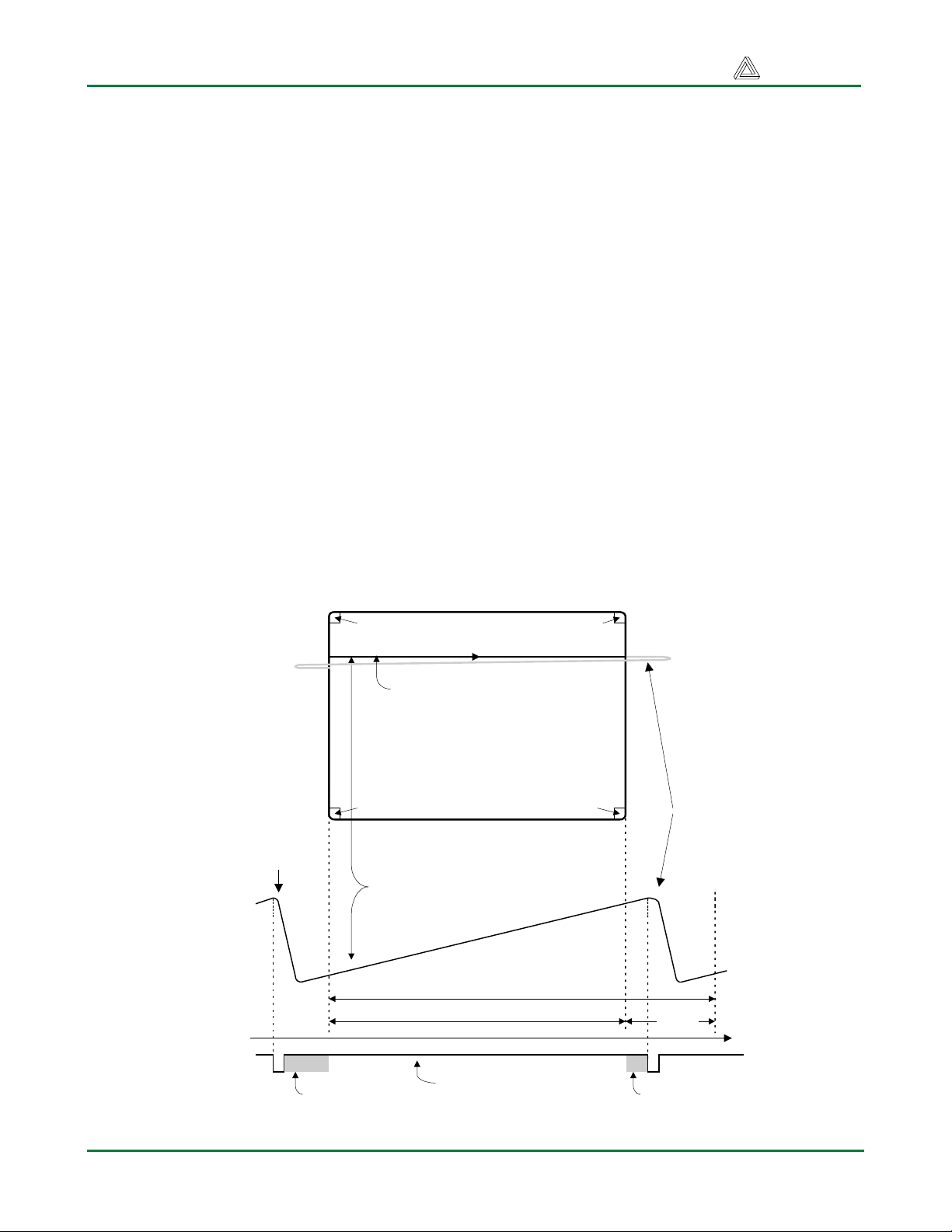
A VGA controller circuit must generate the HS
and VS timings signals and coordinate the
delivery of video data based on the pixel clock.
The pixel clock defines the time available to
display 1 pixel of information. The VS signal
defines the “refresh” frequency of the display, or
Current
through
horizontal
defletion
coil
time
pixel 0,0
640 pixels are displayed each
time the beam travels across
the screen
pixel 0,639
VGA display
surface
pixel 479,0 pixel 479,639
Stable current ramp - information
displayed during this time
Total horizontal time
Horizontal display time
Retrace - no
information
displayed
during this
time
retrace
time
HS
www.digilentinc.com Page 7
Horizontal sync signal
sets retrace frequency
"back porch""front porch"
Page 8
DIO4 Reference Manual Digilent, Inc.
the frequency at which all information on the
display is redrawn. The minimum refresh
frequency is a function of the display’s
phosphor and electron beam intensity, with
practical refresh frequencies falling in the 50Hz
to 120Hz range. The number of lines to be
displayed at a given refresh frequency defines
the horizontal “retrace” frequency. For a 640pixel by 480-row display using a 25MHz pixel
clock and 60 +/-1Hz refresh, the signal timings
shown in the table below can be derived.
Timings for sync pulse width and front and
back porch intervals (porch intervals are the
pre- and post-sync pulse times during which
information cannot be displayed) are based on
observations taken from VGA displays.
Symbol Parameter
T
Sync pulse time
S
T
Display time
disp
T
VS pulse width
pw
T
VS front porch
fp
T
VS back porch
bp
Vertical Sync
Time Clocks Lines
16.7ms
15.36ms
320 us
928 us
64 us
416,800
384,000
1,600
8,000
23,200
521
480
2
10
29
A VGA controller circuit decodes the output of a
horizontal-sync counter driven by the pixel clock
to generate HS signal timings. This counter can
be used to locate any pixel location on a given
row. Likewise, the output of a vertical-sync
counter that increments with each HS pulse can
be used to generate VS signal timings, and this
counter can be used to locate any given row.
These two continually running counters can be
used to form an address into video RAM. No
time relationship between the onset of the HS
pulse and the onset of the VS pulse is specified,
so the designer can arrange the counters to
easily form video RAM addresses, or to minimize
decoding logic for sync pulse generation.
Horizontal Sync
32 us
Clocks
800
640
96
16
48
Time
25.6 us
3.84 us
640 ns
1.92 us
T
S
T
disp
T
pw
T
fp
T
bp
Expansion Connectors
Connector pinouts are shown below.
Separately available tables show pass-through
connections for the devices on the DIO4 board
when it is attached to various system boards.
Note that connectors on system boards and
peripheral boards use the same numbering
scheme – that is, if the board is held with the
component side towards you and the
connectors pointing up, then pin #1 is always
on the bottom left corner of the connector.
This means that when a peripheral board is
plugged into a system board, the numbering
patterns are mirrored. Pin #1 on the peripheral
board mates with pin #39 on the system board,
peripheral board pin #2 mates with system pin
#40, etc. Note that odd pin number mating pairs
add to 40, and even pin number mating pairs
add to 42 (so pin 36 mates with pin 6, pin 27
mates with pin 13, etc.).
www.digilentinc.com Page 8
Page 9

DIO4 Reference Manual Digilent, Inc.
DIO4 Expansion Connector Pinout
P1 Signal Dir P2 Signal Dir
1 nc
2 nc
3 nc
4 nc
5 nc 5 nc
6 nc
7 nc 7 nc
8 nc 8 nc
9 nc 9 nc
10 nc 10 nc
11 nc 11 nc
12 nc 12 nc
13 AN3 in 13 VS
14 AN4 in 14 HS
15 AN1 in 15 GRN
16 AN2 in 16 RED
17 BTN4 out 17 PS2D bidi
18 BTN5 out 18 BLU in
19 nc 19 BTN2 out
20 BTN3 out 20 PS2C bidi
21 LED8 in 21 DP in
22 LEDG
23 LED7
24 nc 24 SW8 out
25 LED6 in 25 CF in
26 nc 26 SW7 out
27 LED5 in 27 CE in
28 nc 28 SW6 out
29 LED4 in 29 CD in
30 nc 30 SW5 out
31 LED3 in 31 CC in
32 nc 32 SW4
33 LED2 in 33 CB in
34 nc 34 SW3 out
35 LED1 in 35 CA in
36 nc 36 SW2 out
37
38 nc 38 SW1
39
40
VCC33
GND
VU
in
in
1 nc
2 nc
3 nc
4 nc
6 nc
in
in
in
in
22 BTN1 out
23 CG in
out
37
39
40
VCC33
GND
VU
www.digilentinc.com Page 9
 Loading...