

Page 1
DDiiggiilleenntt DDIIOO22
RReeffeerreennccee MMaannuuaal
Revision: 5/7/02 215 E Main Suite D | Pullman, WA 99163
l
www.digilentinc.com
(509) 334 6306 Voice and Fax
Overview
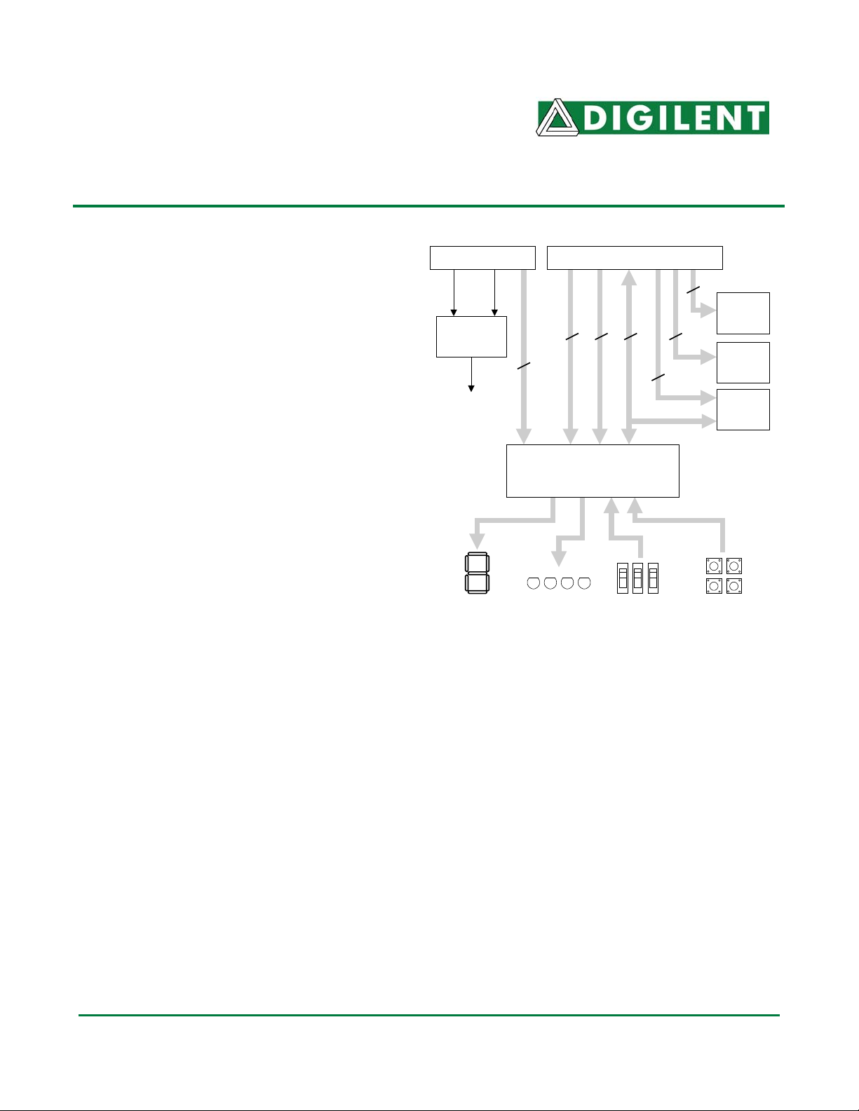
The Digilab Digital I/O board 2 (the DIO2) is
one of several expansion boards designed to
mate with Digilab system boards. The DIO2
board provides an assortment of frequently
used digital I/O devices, many of which are
controlled by an on-board Xilinx XC95108
CPLD. The CPLD also provides a bus interface
VU
5VDC
regulator
VDD
GND
4
JTAG
Connector BConnector A
6
control
address
2
PS2
8
4
data
10
3
port
VGA
port
16x2
LCD
to simplify communications with Digilab
system boards. DIO2 boards can be combined
with Digilab system boards to implement
projects ranging from basic logic designs to
XC95108
PC84
general computer systems, without the need for
any other components.
DIO2 board features include:
• A XC95108 CPLD for I/O device and
system bus control;
• A 16x2 character LCD with integral
Samsung controller IC;
4 7-seg.
displays
15 LEDs
DIO2 circuit board block diagram
8 switches
15 button
keypad
• A four digit seven-segment LED display;
• 16 individual LEDs of various colors;
• An 8-bit VGA port;
• A 15-button keypad;
• 8 slide switches;
• A PS2 mouse/keyboard port;
• An on board 5VDC regulator.
The CPLD comes pre-configured with the
circuit shown in Appendix 1, but it can also be
reprogrammed from any Xilinx CAD tool,
including the free WebPack tools available
from the Xilinx website. CPLD configuration
can be accomplished using the Xilinx JTAG
cable or the Digilent XC95 programming
board.
Doc: 502-005 page 1 of 19
Copyright Digilent, Inc. All rights reserved. Other product and company names mentioned may be trademarks of their respective owners.
®
Page 2
Digilab DIO2 Reference Manual Digilent, Inc.
Functional description
The DIO2 board includes many frequently used peripheral devices found in digital systems, including
several output display devices and several input devices. When mated with a Digilab main board, the
DIO2 board provides a highly flexible digital system development platform. The DIO2 board centers
on a Xilinx XC95108 CPLD that provides a convenient interface to most of the I/O devices, as well as
a control bus between an attached system board and the I/O devices. Since the CPLD on the DOI2
board is user configurable, many different I/O control and communication schemes can easily be
implemented.
Although the DIO2 board has been designed as a peripheral board for various Digilab system boards, it
can also be used as a CPLD demonstration/development board. Digilent produces a low cost power
supply/programming board that can be connected to the DIO2 board to create a stand-alone, very low
cost CPLD platform. This board, called the DXC95 board, provides a JTAG programming interface, a
power supply, a clock source, and a small breadboard area (see www.digilentinc.com for more
information).
This document presents the
circuits, I/O devices, and
interfaces in the DIO2 board.
When needed, manufacturer part
numbers have been provided so
that further reference material
can be obtained from their
websites.
Signals
All named signals used on the
DIO2 board are defined in the
table on the right. Voltage levels
for all signals arriving from an
attached Digilab system board
are determined by the system
board, but all signals arising on
the I/O board derive from the
on-board 5VDC regulator (so
they are all 5V CMOS signals).
The DIO2 board uses a twolayer process, so all signals are
available on the top and bottom
layers. Many signals are brought
to a test point header for easy
test and measurement equipment
attachment.
Power Supplies
VU Unregulated power supply voltage from attached system
board – typically 5-9VDC. Available only on J1 P40, this
supply is regulated to 5VDC to supply on onboard devices.
VDD* Regulated power supply voltage (5VDC) from on-board
regulator. This supply is used by all devices on DIO2 board.
GND* System ground
CPLD – system board bus signals
D7-D0* Bi-directional data bus between B connector and CPLD/LCD
A5-A0* Address lines to select locations in CPLD
CS* Chip select used for CPLD interface on DIO2 board
WE* Write enable for CPLD memory locations
OE* Output enable for CPLD data signals
BOCI* “Button Out-Clock In” pin, used as clock input to CPLD
LCD control signals
D7-D0 Data bus – same as CPLD data signals
LCD_RW* LCD Read/Write signal – ‘1’ for read mode
LCD_RS* LCD Register Select – ‘1’ for data register, ‘0’ for instruction
LCD_E LCD Enable signal – active high; falling edge latches data
VGA and PS2 signals (routed directly from B connector, not through CPLD)
HS* VGA Horizontal Sync signal
VS* VGA Vertical Sync signal
R1, R0* VGA 2-bit red data
G2-G0* VGA 3-bit green data
B2-B0* VGA 3-bit blue data
KCLK* PS2 (Keyboard or Mouse) clock signal
KDAT* PS2 (Keyboard or Mouse) data signal
On board devices (routed through CPLD)
BTN0-E Pushbuttons (A through E)
SW1-SW8 Slide switches (1 through 8)
LD0-LDF Discreet LEDs (0 through F)
CA-CF Seven-segment display cathodes
AN1-AN3 Seven-segment display anodes
* available on test point header
Table 1. DIO2 board signal definitions
www.digilentinc.com page 2 of 19
Copyright Digilent, Inc. All rights reserved. Other product and company names mentioned may be trademarks of their respective owners.
Page 3
Digilab DIO2 Reference Manual Digilent, Inc.
Power Supplies
The DIO2 board receives system power from pins 39 and 40 of connector A. Pin 40 is connected
directly to a 5VDC LDO regulator (an LM2940), and pin 39 is connected to ground. The regulator
powers all devices on the DIO2 board, including the CPLD (all outbound data signals from the DIO2
board are 5V). The regulator requires about 400mV of dropout voltage, so a DC voltage 5.5VDC 8VDC must be applied to pin 40 of connector A for proper board operation.
Digilab system boards route unregulated voltage directly from the power supply to pin 2 of all
expansion connectors. Since pin 2 on system boards mates with pin 40 on expansion boards, the DIO2
board receives power from the supply attached to the system board.
With no LED’s illuminated, the DIO2 board typically consumes about 200mA. With all LEDs
illuminated (including all segments of the seven-segment display), the board can consume up to
350mA.
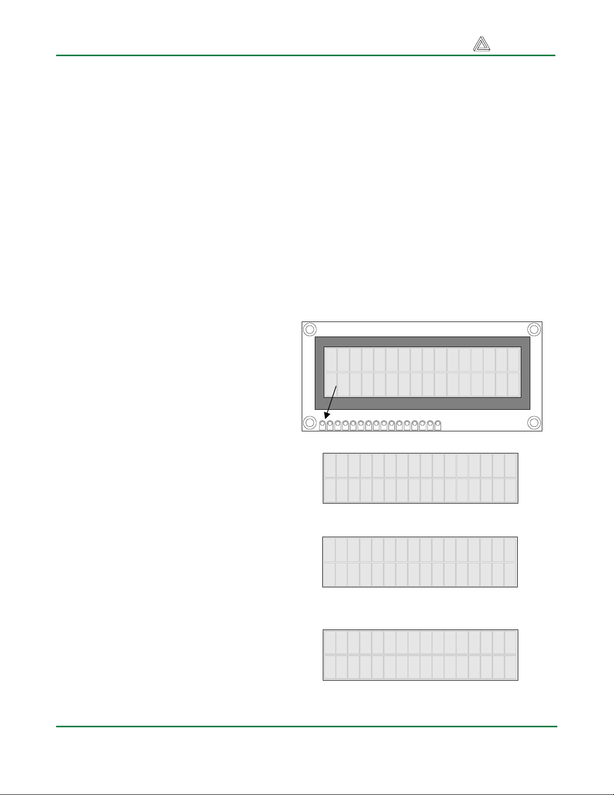
LCD
The LCD display is a 16 character, 2 line
display from the Okaya company (Okaya part
number RC1602D). The Okaya data sheet may
be found on the Digilent website.
Pin 1
16 x 2 character LCD
The display uses a KS0066 Samsung controller
that has a character-generator ROM (CGROM)
containing 208 preset 5x8 character patterns, a
character-generator RAM (CGRAM) that can
hold 8 user-defined 5x8 characters, and a display
data RAM (DDRAM) that can hold 80 character
00 01 02 03 04 05 06 07 08 09 0A 0B 0C 0D 0E 0F
codes. Character codes written into the DDRAM
serve as indexes into the CGROM (or CGRAM).
Writing a character code into a particular DDRAM
location will cause the associated 5x8 character
40 41 42 43 44 45 46 47 48 49 4A 4B 4C 4D 4E 4F
DDRAM address - display postion map
pattern to appear at the corresponding display
location. The display positions can be shifted left
01 02 03 04 05 06 07 08 09 0A 0B 0C 0D 0E 0F
10
or right by setting a bit in the instruction register
(IR). The write-only IR is used to direct display
41 42 43 44 45 46 47 48 49 4A 4B 4C 4D 4E 4F
50
operations (such as clear display, shift left or right,
set DDRAM address, etc). Available instructions
are shown in the rightmost column of the table
DDRAM address - display postion map
after shift-left operation
below, together with the IR codes. A busy flag is
00 01 02 03 04 05 06 07 08 09 0A 0B 0C 0D 0E
available to indicate whether the display has
competed the last requested operation; prior to
initiating a new operation, the flag can be checked
to see whether the previous operation has been
completed.
27
40 41 42 43 44 45 46 47 48 49 4A 4B 4C 4D 4E
67
DDRAM address - display postion map
after shift-right operation
www.digilentinc.com page 3 of 19
Copyright Digilent, Inc. All rights reserved. Other product and company names mentioned may be trademarks of their respective owners.
Page 4
Digilab DIO2 Reference Manual Digilent, Inc.
The display has more DDRAM locations than can be displayed at any given time. DDRAM locations
00H to 27H map to the first display row, and locations 40H to 67H map to the second row. Normally,
DDRAM location 00H maps to the upper left display corner, and 40H to the lower left. Shifting the
display left or right can change this mapping. The display uses a temporary data register (DR) to hold
data during DDRAM /CGRAM read or write operations, and an internal address register to select the
RAM location. Address register contents, which can be set via the IR, are automatically incremented
after each read or write operation. The LCD display uses ASCII character codes. Codes up through 7F
are standard ASCII (which includes all “normal” alphanumeric characters). Codes above 7F produce
various international characters – please see the manufacturers data sheet for more information on
international codes.
Display Instructions and Instruction Codes
Instruction
Clear
Display
Return
Home
Entry mode
set
Display
ON/OFF
control
Cursor or
Display shift
Function Set 0 0 0 0 1 DL N F X X
Set CGRAM
Address
Set DDRAM
address
Read busy
flag/ address
Write data
to RAM
Read data
from RAM
RS R/W DB7 DB6 DB5 DB4 DB3 DB2 DB1 DB0
0 0 0 0 0 0 0 0 0 1
0 0 0 0 0 0 0 0 1 X
0 0 0 0 0 0 0 1 I/D SH
0 0 0 0 0 0 1 D C B
0 0 0 0 0 1 S/C R/L X X
0 0 0 1 AC5 AC4 AC3 AC2 AC1 AC0 Set CGRAM address counter
0 0 1 AC6 AC5 AC4 AC3 AC2 AC1 AC0 Set DDRAM address counter
0 1 BF AC6 AC5 AC4 AC3 AC2 AC1 AC0
1 0 D7 D6 D5 D4 D3 D2 D1 D0
1 1 D7 D6 D5 D4 D3 D2 D1 D0
Instruction bit assignments
Clear display by writing a 20H to
all DDRAM locations; set
DDRAM address register to 00H;
and return cursor to home.
Return cursor to home (upper left
corner), and set DDRAM address
to 0H. DDRAM contents not
changed.
I/D = ‘1’ for right-moving cursor
and address increment; SH = ‘1’
for display shift (direction set by
I/D bit).
Set display (D), cursor (C), and
blinking cursor (B) on or off.
SC = ‘0’ to shift cursor right or
left, ‘1’ to shift entire display
right or left (R/L = ‘1’ for right).
Set interface data length (DL =
‘1’ for 8 bit), number of display
lines (N = ‘1’ for 2 lines), display
font (F = ‘0’ for 5x 8 dots)
Read busy flag and address
counter
Write data into DDRAM or
CGRAM, depending on which
address was last set
Read data from DDRAM or
CGRAM, depending on which
address was last set
Description
www.digilentinc.com page 4 of 19
Copyright Digilent, Inc. All rights reserved. Other product and company names mentioned may be trademarks of their respective owners.
Page 5
Digilab DIO2 Reference Manual Digilent, Inc.
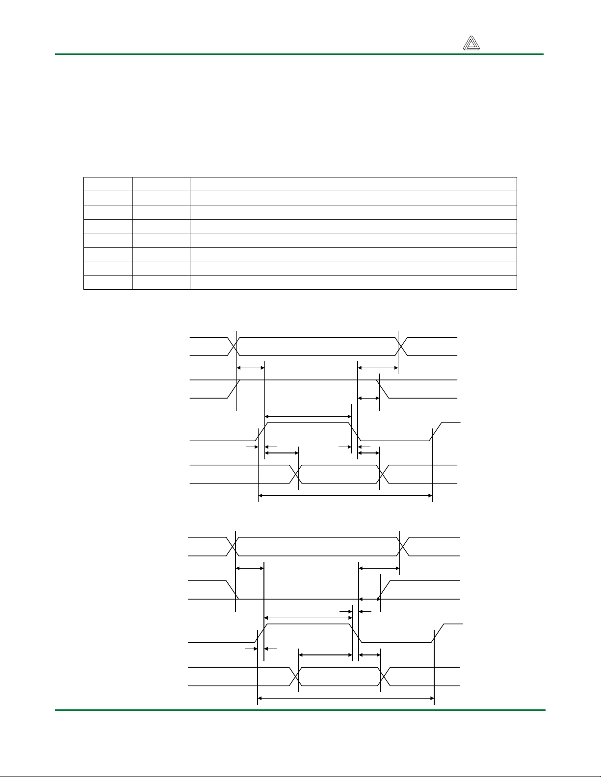
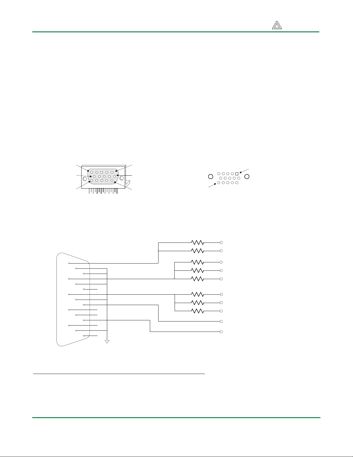
The display is connected to the DIO2 board by a 16-pin connector (pins 15 and 16 are for an optional
backlight, and they are not connected on the DIO2 board). The eight data bus signals and three strobes
are connected directly to the B connector on the DIO2 board (note the data lines are common with the
CPLD data bus), so the LCD can be controlled from a Digilab system board. Bus timings are shown
below. Note that the enable signal (E) serves as both output enable and write strobe (with an active
falling edge) depending on the state of the Read/Write (R/W) signal.
Pin No. Symbol Signal Description
1 Vss Signal ground
2 Vdd Power supply (5V)
3 Vo Operating (contrast) voltage (LCD drive, typically 100mV at 20C)
4 RS Register select: high for data transfer, low for instruction register
5 R/W Read/write signal: high for read mode, low for write mode
6 E Read/write strobe: high for read OE; falling edge writes data
7-14 Data Bus Bi-directional data bus
LCD Read Cycle
LCD Write Cycle
RS
R/W
DB0-DB7
RS
R/W
tsu
tw
E
tr tf
tD tDH
tc
th
th
tsu
tw
tf
th
th
E
tr
DB0-DB7
tsu1 th1
tc
www.digilentinc.com page 5 of 19
Copyright Digilent, Inc. All rights reserved. Other product and company names mentioned may be trademarks of their respective owners.
Page 6
Digilab DIO2 Reference Manual Digilent, Inc.
Parameter Symbol Min Max Unit Test Pin
Enable cycle time tc 500 ns E
Enable High pulse width tw 220 ns E
Enable rise/fall time tr, tf 25 ns E
RS, R/W setup time tsu 40 ns RS, R/W
RS, R/W hold time th 10 ns RS, R/W
Read data output delay tD 60 120 ns DB0-DB7
Read data hold time tDH 20 ns DB0-DB7
Write data setup time tsu1 40 ns DB0-DB7
Write data hold time th1 10 ns DB0-DB7
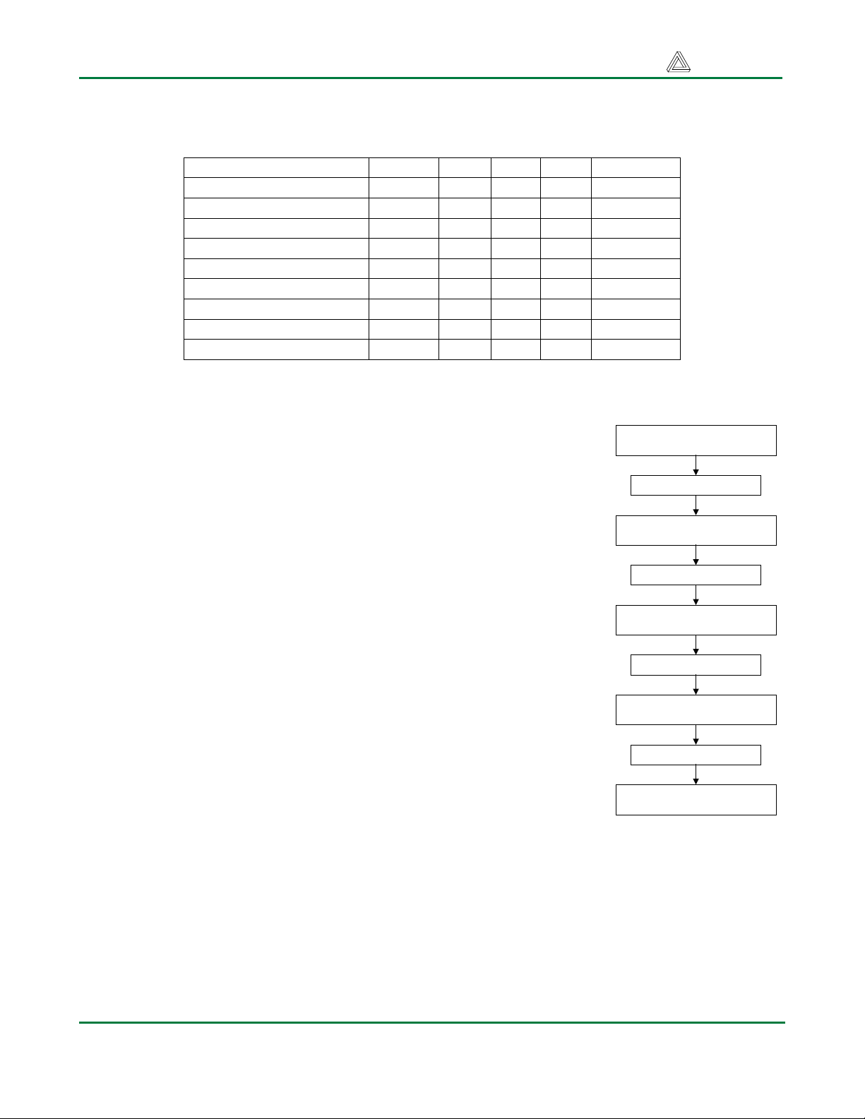
LCD start-up sequence
The manufacturer requires that a startup sequence with specific timings be
Power On
followed to ensure proper LCD operation. After power-on, at least 20ms
must elapse before the function-set instruction code can be written to set the
Wait for 20ms
bus width, number of lines, and character patterns (8-bit interface, 2 lines,
and 5x8 dots are appropriate). After the function-set instruction, at least
Function Set
37us must elapse before the display-control instruction can be written (to
turn the display on, turn the cursor on or off, and set the cursor to blink or
no blink). Then after another 37us, the display-clear instruction can be
Wait for 37us
issued, followed by a 1.52ms delay. Finally, the entry-mode instruction code
can be used to set address increment (or address decrement) mode, and
Display Control Set
display shift mode (on or off). Once this sequence is complete, data can be
written into the DDRAM to cause information to appear on the display.
Wait for 37us
LEDs
Display Clear
Sixteen individual LEDs (8 red, 4 yellow, and 4 green) are provided for
circuit outputs. The LED cathodes are driven directly from the CPLD, and
Wait for 1.52ms
the anodes are tied to Vdd via 270-ohm resistors (so the LED drive signals
are active low). When the CPLD is configured with the code shown in the
appendix, two 8-bit registers at locations x04 and x05 drive the LED
cathode signals. Note the LED signals are inverted in the VHDL code, so a
OK for operati o ns
LCD startup sequence
logic “1” turns on the LEDs.
Seven-segment LED display
The DIO2 board contains a modular 4-digit, common anode, seven-segment LED display. In a
common anode display, the seven anodes of the LEDs forming each digit are connected to four
common circuit nodes (labeled AN1 through AN4 on the DIO2 board). Each anode, and therefore each
digit, can be independently turned on and off by driving these signals to a ‘1’ or a ‘0’. The cathodes of
www.digilentinc.com page 6 of 19
Copyright Digilent, Inc. All rights reserved. Other product and company names mentioned may be trademarks of their respective owners.
Page 7

Digilab DIO2 Reference Manual Digilent, Inc.
similar segments on all four displays are also connected together into seven common circuit nodes
labeled CA through CG. Thus, each cathode for all four displays can be turned on and off
independently.
Common anode
a
f
e
Figure 4.
(b) common anode display configuration. (c)
segement illumination patterns for decimal.
digits. (d) segment illumination truth table.
b
g
c
d
(a) (b)
(a) Seven segment display detail.
afgedcb
(c)
Digit
Shown
0
1
2
3
4
5
6
7
8
9
Illuminated Segment
a b c d e f g
1 1 1 1 1 1 0
0 1 1 0 0 0 0
1 1 0 1 1 0 1
1 1 1 1 0 0 1
0 1 1 0 0 1 1
1 0 1 1 0 1 1
1 0 1 1 1 1 1
1 1 1 0 0 0 0
1 1 1 1 1 1 1
1 1 1 1 0 1 1
(d)
This connection scheme creates a multiplexed display, where a 4digit display can be created by driving the anode signals and
corresponding cathode patterns of each digit in a repeating,
continuous succession. In order for each of the four digits to appear
bright and continuously illuminated, all four digits should be driven
Anodes
via transistors for greater current
-- connected to CPLD
Vdd
a2
a3a4
a1
once every 1 to 16ms (for a refresh frequency of 60Hz to 1KHz).
For example, in a 60Hz refresh scheme, each digit would be
illuminated for ¼ of the refresh cycle, or 4ms. The controller must
assure that the correct cathode pattern is present when the
corresponding anode signal is driven. To illustrate the process, if
AN1 is driven high while CB and CC are driven low, then a “1”
will be displayed in digit position 2. Then, if AN2 is driven high
while CA, CB and CC are driven low, then a “7” will be displayed
in digit position 2. If AN1/CB, CC are driven for 4ms, and then
AN2/CA, CB, CC are driven for 4ms in an endless succession, the
abcdefgdp
Cathodes
CPLD pins via 100
-- connected to
Ω
resistor
display will show “17” in the first
two digits. An example timing
Refresh period = 1ms to 16ms
diagram is provided below.
When configured with the code
shown in the appendix, the CPLD
on the DIO2 board implements a
seven-segment controller provided
AN1
AN2
AN3
Digit period = Refresh / 4
a suitable clock (256Hx to 1KHz)
is provided on the CLK_IN pin.
AN4
The controller accepts four 4-bit
binary numbers in two successive
registers (at addresses 6 and 7), and
decodes and displays them.
Cathodes
Seven segment display refresh signals and timings
Digit 1 Digit 2 Digit 3 Digit 4
www.digilentinc.com page 7 of 19
Copyright Digilent, Inc. All rights reserved. Other product and company names mentioned may be trademarks of their respective owners.
Page 8
Digilab DIO2 Reference Manual Digilent, Inc.
D
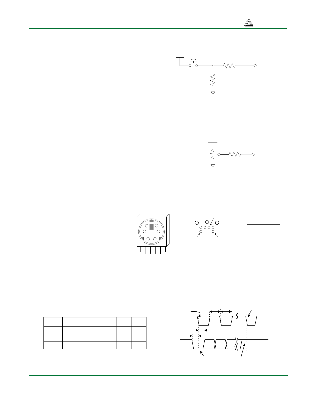
Pushbuttons
Outputs from the 15 momentary-contact push buttons
are normally low, and are driven high only while the
button is actively pressed. The buttons exhibit a worstcase bounce time of about 1ms. A 4.7K series resistor
provides some debounce filtering and ESD protection.
Vdd
RP8&9
4.7KOhm
To CPLD
RP10,12,14,16
4.7KOhm
When configured with the code shown in the
appendix, the CPLD on the DIO2 board makes all
GND
button signals available on the bus in two successive
readable address locations (0 and 1).
Switches
The eight slide switches can be used to connect either Vdd or
GND to eight pins on the CPLD. The switches exhibit about 2ms
of bounce, and no active debouncing circuit is employed. A 4.7K-
Vdd
RP6 & 7
4.7 KOhm
To CPL
ohm series resistor is used for nominal input protection. When
configured with the code shown in the appendix, the CPLD on the
GND
DIO2 board makes all switch signals available on the bus at
address location 2.
PS2 port
The DIO2 board includes a 6-pin
mini-DIN connector that can
accommodate a PS2 mouse or PS2
keyboard connection. Both the
mouse and keyboard use a twowire serial bus (including clock
and data) to communicate with a
host device, and both drive the bus
2
4
PS2 Connector front view
1
6
3
5
Pin 1
Pin 5Pin 6
Bottom-up
hole pattern
PS2 Pin Definitions
Pin Function
1 Data
2 Reserved
3 GND
4 Vdd
5 Clock
6 Reserved
with identical signal timings. Both
use 11-bit words that include a start, stop and odd parity bit, but the data packets are organized
differently, and the keyboard interface allows bi-directional data transfers (so the host device can
illuminate state LEDs on the keyboard).
T
T
CK
Symbol Parameter Min Max
T
Clock time
CK
T
Data-to-clock setup time
SU
T
Clock-to-data hold time 5us 25us
HLD
30us
5us
50us
25us
Edge 0
CLK
DATA
CK
T
T
SU
HLD
'1' stop bit'0' start bit
Edge 10
www.digilentinc.com page 8 of 19
Copyright Digilent, Inc. All rights reserved. Other product and company names mentioned may be trademarks of their respective owners.
Page 9

Digilab DIO2 Reference Manual Digilent, Inc.
Bus timings are shown below. The clock and data signals are only driven when data transfers occur,
and otherwise they are held in the “idle” state at logic ‘1’. The timings define signal requirements for
mouse-to-host communications and bi-directional keyboard communications.
Keyboard
The keyboard uses open collector drivers so that either the keyboard or an attached host device can
drive the two-wire bus (if the host device will not send data to the keyboard, then the host can use
simple input-only ports). On the DIO2 board, the clock and data signals (PS2C and PS2D) bypass the
CPLD, and are connected directly to pins on the B connector.
A PS2-style keyboard uses scan codes to communicate key press data (nearly all keyboards in use
today are PS2 style). Each key has a single, unique scan code that is sent whenever the corresponding
key is pressed. If the key is pressed and held, the scan code will be sent repeatedly once every 100ms
or so. When a key is released, a “F0” key-up code is sent, followed by the scan code of the released
key. If a key has a “shift” character that is different than the non-shift character, the same scan code is
sent whether the shift key is pressed or not, and the host device must determine which character to use.
Some keys, called extended keys, send an “E0” ahead of the scan code (and they may send more than
one scan code). When an extended key is released, a “E0 F0” key-up code is sent, followed by the scan
code. Scan codes for most keys are shown in the figure below.
ESC
76
` ~
0E
TAB
0D
Caps Lock
58
Shift
12
Ctrl
14
F105F206F304F4
0C
1 !162 @1E3 #264 $255 %
2E
Q
15W1DE24R2DT2C
A
1CS1BD23F2BG34
Z
1ZX22C21V2AB32
Alt
11
F503F60BF783F8
0A
6 ^367 &3D8 *3E9 (460 )45- _4E= +55BackSpace
Y
35U3CI43O44P4D
H
33J3BK42L4B
N
31M3A
Space
29
, <41> .49/ ?
F901F1009F1178F12
07
66
; :
4C
4A
Alt
E0 11
[ {54] }
5B
' "
52
\ |
5D
Enter
5A
Shift
59
Ctrl
E0 14
E0 75
E0 74
E0 6B
E0 72
A host device can also send data to the keyboard. Below is a short list of some often-used commands.
ED Turn on/off Num Lock, Caps Lock, and Scroll Lock LEDs. The keyboard acknowledges receipt
of an “ED” by returning an “FA”, after which the host send another byte to set LED status: Bit 0
sets Scroll Lock; bit 1 sets the Num Lock; and Bit 2 sets Caps lock. Bits 3 to 7 are ignored.
EE Echo. Upon receiving an echo command, the keyboard replies with the same scan code (“EE”).
F3 Set scan code repeat rate. The keyboard acknowledges receipt of an “F3” by returning an “FA”,
after which the host sends a second byte to set the repeat rate.
FE Resend. Upon receiving a resend command, the keyboard will re-send the last scan code sent.
FF Reset. Resets the keyboard.
www.digilentinc.com page 9 of 19
Copyright Digilent, Inc. All rights reserved. Other product and company names mentioned may be trademarks of their respective owners.
Page 10
Digilab DIO2 Reference Manual Digilent, Inc.
The keyboard should send data to the host only when both the data and clock lines are high (or idle).
Since the host is the “bus master”, the keyboard should check to see whether the host is sending data
before driving the bus. To facilitate this, the clock line can be used as a “clear to send” signal. If the
host pulls the clock line low, the keyboard must not send any data until the clock is released (host-tokeyboard data transmission will not be dealt with further here).
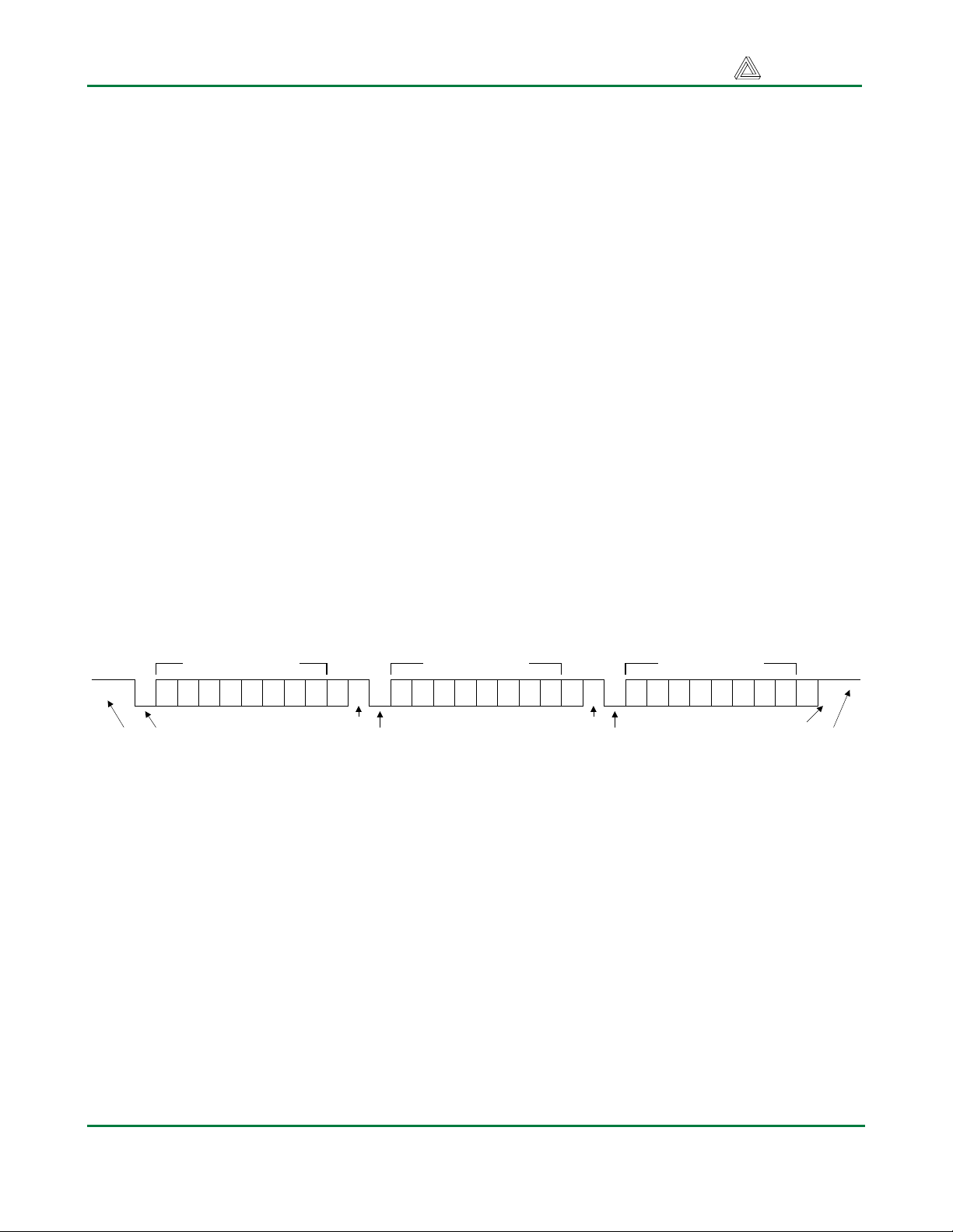
The keyboard sends data to the host in 11-bit words that contain a ‘0’ start bit, followed by 8-bits of
scan code (LSB first), followed by an odd parity bit and terminated with a ‘1’ stop bit. The keyboard
generates 11 clock transitions (at around 20 - 30KHz) when the data is sent, and data is valid on the
falling edge of the clock.
Mouse
The mouse outputs a clock and data signal when it is moved; otherwise, these signals remain at logic
‘1’. Each time the mouse is moved, three 11-bit words are sent from the mouse to the host device. Each
of the 11-bit words contains a ‘0’ start bit, followed by 8 bits of data (LSB first), followed by an odd
parity bit, and terminated with a ‘1’ stop bit. Thus, each data transmission contains 33 bits, where bits
0, 11, and 22 are ‘0’ start bits, and bits 11, 21, and 33 are ‘1’ stop bits. The three 8-bit data fields
contain movement data as shown below. Data is valid at the falling edge of the clock, and the clock
period is 20 to 30KHz.
Mouse status byte X direction byte Y direction byte
L R 0 1 XS YS XY YY P X0 X1 X2 X3 X4 X5 X6 X7 P Y0 Y1 Y2 Y3 Y4 Y5 Y6 Y7 P
Start bit Stop bit
Idle state
10 100 11
Start bit
Stop bit
Start bit
Stop bit
Idle state
The mouse assumes a relative coordinate system wherein moving the mouse to the right generates a
positive number in the X field, and moving to the left generates a negative number. Likewise, moving
the mouse up generates a positive number in the Y field, and moving down represents a negative
number (the XS and YS bits in the status byte are the sign bits – a ‘1’ indicates a negative number).
The magnitude of the X and Y numbers represent the rate of mouse movement – the larger the number,
the faster the mouse is moving (the XV and YV bits in the status byte are movement overflow
indicators – a ‘1’ means overflow has occurred). If the mouse moves continuously, the 33-bit
transmissions are repeated every 50ms or so. The L and R fields in the status byte indicate Left and
Right button presses (a ‘1’ indicates the button is being pressed).
www.digilentinc.com page 10 of 19
Copyright Digilent, Inc. All rights reserved. Other product and company names mentioned may be trademarks of their respective owners.
Page 11
Digilab DIO2 Reference Manual Digilent, Inc.
VGA port
The five standard VGA signals Red (R), Green (G), Blue (B), Horizontal Sync (HS), and Vertical Sync
(VS) are routed directly from the B connector to the VGA connector, bypassing the CPLD. A resistordivider network is used to provide 8-bit color, with 3 bits for blue, 3 bits for green, and 2 bits for red
(the human eye is less sensitive to red, so red got 2 bits instead of 3). The resistor network uses the 75
ohm VGA cable termination to ensure that the color signals remain in the VGA-specified 0V – 0.7V
range. The HS and VS signals are TTL level, and come directly from the FPGA via the B connector.
VGA signal timings are specified, published, copyrighted and sold by the VESA organization
(www.vesa.org). The following VGA system and timing information is provided as an example of how
a VGA monitor might be driven in 640 by 480 mode. For more precise information, or for information
on higher VGA frequencies, refer to document available at the VESA website (or experiment!).
Pin 5
Pin 10
Pin 15
Pin 1
Pin 6
Pin 11
Pin 1
Pin 15
DB15 VGA connector
Front view
DB15 through-hole pattern as
seen from the top
1
6
2
7
3
8
4
9
5
10
DB15
Connector
11
12
13
14
15
Red
Green
Blue
Horizontal Sync
Vertical Sync
512
1K
512
1K
2K
512
1K
2K
To R0 on Connector B
To R1 on Connector B
To G0 on Connector B
To G1 on Connector B
To G2 on Connector B
To B0 on Connector B
To B1 on Connector B
To B2 on Connector B
To HS on Connector B
To VS on Connector B
GND
VGA systems and signal timings for a 60Hz, 640x480 display
CRT-based VGA displays use amplitude modulated, moving electron beams (or cathode rays) to
display information on a phosphor-coated screen. LCD displays use an array of switches that can
impose a voltage across a small amount of liquid crystal, thereby changing light permitivity through
the crystal on a pixel-by-pixel basis. Although the following description is limited to CRT displays,
www.digilentinc.com page 11 of 19
Copyright Digilent, Inc. All rights reserved. Other product and company names mentioned may be trademarks of their respective owners.
Page 12
Digilab DIO2 Reference Manual Digilent, Inc.
LCD displays have evolved to use the same signal timings as CRT displays (so the “signals”
discussion below pertains to both CRTs and LCDs).
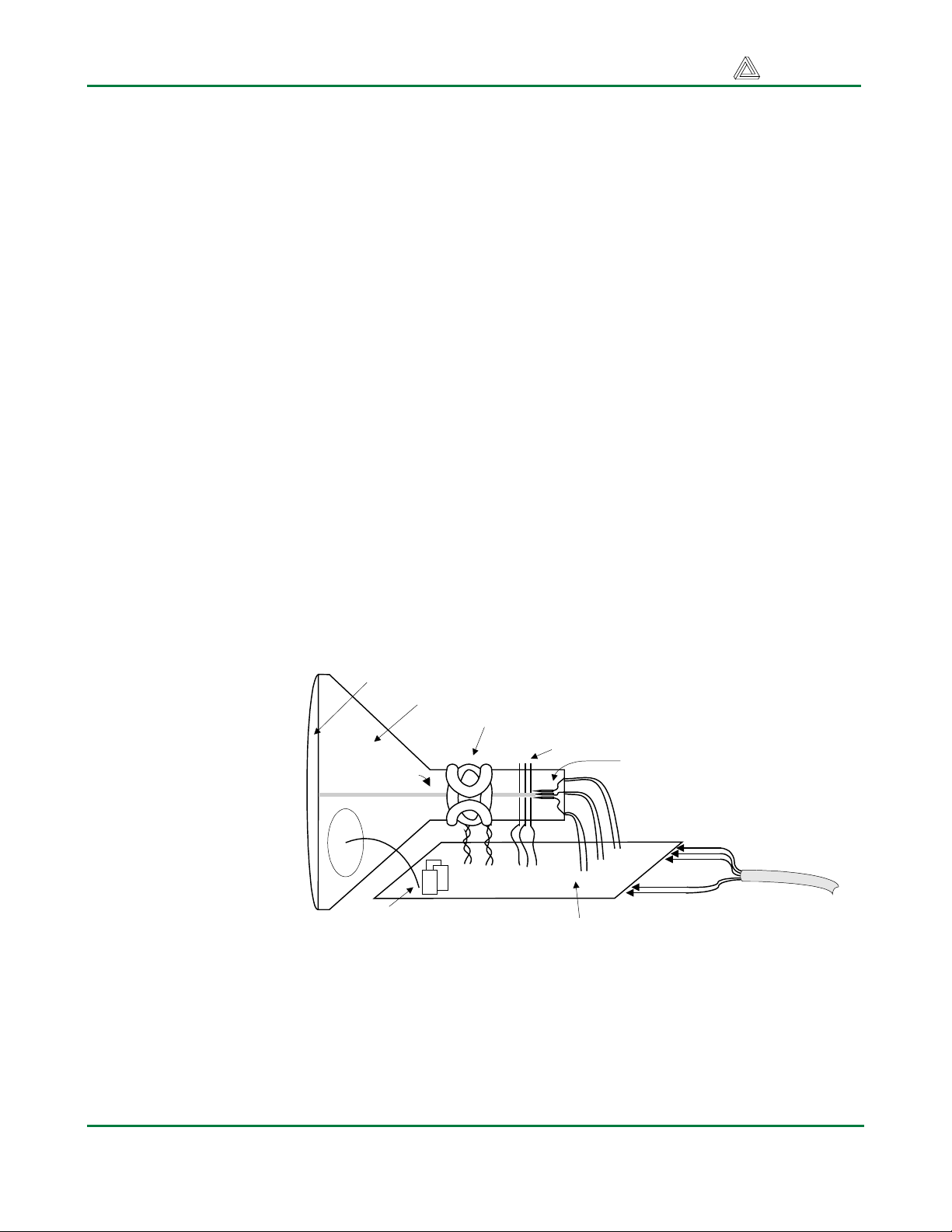
CRT displays use electron beams (one for red, one for blue and one for green) to illuminate phosphor
that coats the inner side of the display end of a cathode ray tube (see drawing below). Electron beams
emanate from “electron guns”, which are a finely pointed, heated cathodes placed in close proximity to
a positively charged annular plate called a “grid”. The electrostatic force imposed by the grid pulls
away rays of energized electrons as current flows into the cathodes. These particle rays are initially
accelerated towards the grid, but they soon fall under the influence of the much larger electrostatic
force that results from the entire phosphor coated display surface of the CRT being charged to 20kV
(or more). The rays are focused to a fine beam as they pass through the center of the grids, and then
they accelerate to impact on the phosphor coated display surface. The phosphor surface glows brightly
at the impact point, and the phosphor continues to glow for several hundred microseconds after the
beam is removed. The larger the current fed into the cathode, the brighter the phosphor will glow.
Between the grid and the display surface, the beam passes through the neck of the CRT where two
coils of wire produce orthogonal electromagnetic fields. Because cathode rays are composed of
charged particles (electrons), they can be bent by these magnetic fields. Current waveforms are passed
through the coils to produce magnetic fields that cause the electron beams to transverse the display
surface in a “raster” pattern, horizontally from left to right and vertically from top to bottom.
Information is only displayed when the beam is moving in the “forward” direction (left to right and top
to bottom), and not during the time the beam is reset back to the left or top edge of the display. Much
of the potential display time is therefore lost in “blanking” periods when the beam is reset and
stabilized to begin a new horizontal or vertical display pass.
The size of the beams,
the frequency at which
the beam can be traced
across the display, and
the frequency at which
the electron beam can be
modulated determine the
Anode (entire screen)
Cathode ray
Cathode ray tube
Deflection coils
Grid
Electron guns
(Red, Blue, Green)
display resolution.
Modern VGA displays
can accommodate
different resolutions, and
a VGA controller circuit
dictates the resolution by
producing timing signals
to control the raster
patterns. The controller
High voltage supply
(>20kV)
deflection
control
Cathode ray tube display system
grid
control
Control board
gun
control
Sync signals
(to deflection control)
R,G,B signals (to guns)
VGA cable
must produce TTL-level synchronizing pulses to set the frequency at which current flows through the
deflection coils, and it must ensure that pixel (or video) data is applied to the electron guns at the
correct time. Video data typically comes from a video refresh memory, with one or more bytes
assigned to each pixel location (the DIO2 board uses 8-bits per pixel). The controller must index into
video memory as the beams move across the display, and retrieve and apply video data to the display
at precisely the time the electron beam is moving across a given pixel.
www.digilentinc.com page 12 of 19
Copyright Digilent, Inc. All rights reserved. Other product and company names mentioned may be trademarks of their respective owners.
Page 13

Digilab DIO2 Reference Manual Digilent, Inc.
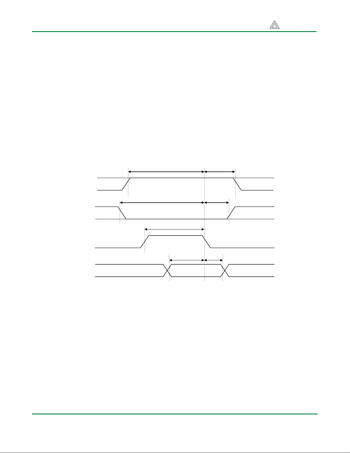
o
The VGA controller circuit
must generate the HS and VS
pixel 0,0
pixel 0,639
timings signals and coordinate
the delivery of video data based
on the pixel clock. The pixel
clock defines the time available
640 pixels are displayed each time
the beam travels across the screen
to display 1 pixel of
information. The VS signal
defines the “refresh” frequency
of the display, or the frequency
at which all information on the
display is redrawn. The
minimum refresh frequency is
a function of the display’s
phosphor and electron beam
Current
through
horizontal
defletion
coil
pixel 479,0 pixel 479,639
Stable current ramp - information
displayed during this time
VGA display
surface
Retrace - n
information
displayed
during this
time
intensity, with practical refresh
frequencies falling in the 60Hz
to 120Hz range. The number of
lines to be displayed at a given
refresh frequency defines the
time
Horizontal display time
Total horizontal time
retrace time
horizontal “retrace” frequency.
For a 640-pixel by 480-row
display using a 25MHz pixel
HS
Horizontal sync signal
sets retrace frequency
"back porch""front porch"
clock and 60 +/-1Hz refresh,
the following signal timings can be derived. Timings for sync pulse width and front and back porch
intervals (porch intervals are the pre- and post-sync pulse times during which information cannot be
displayed) are based on observations taken from VGA displays.
VGA Signal Timing
Symbol Parameter
T
Sync pulse time
S
T
disp
T
pw
T
fp
T
bp
Display time
VS pulse width
VS front porch
VS back porch
Vertical Sync
Time Clocks Lines
16.7ms
15.36ms
320 us
928 us
64 us
416,800
384,000
1,600
8,000
23,200
Horizontal Sync
Time
521
480
25.6 us
2
3.84 us
10
640 ns
29
1.92 us
32 us
Clocks
800
640
96
16
48
T
S
T
disp
T
pw
T
fp
T
bp
A VGA controller circuit decodes the output of a horizontal-sync counter driven by the pixel clock to
generate HS signal timings. This counter can be used to locate any pixel location on a given row.
Likewise, the output of a vertical-sync counter that increments with each HS pulse can be used to
generate VS signal timings, and this counter can be used to locate any given row. These two
continually running counters can be used to form an address into video RAM. No time relationship
www.digilentinc.com page 13 of 19
Copyright Digilent, Inc. All rights reserved. Other product and company names mentioned may be trademarks of their respective owners.
Page 14

Digilab DIO2 Reference Manual Digilent, Inc.
between the onset of the HS pulse and the onset of the VS pulse is specified, so the designer can
arrange the counters to easily form video RAM addresses, or to minimize decoding logic for sync
pulse generation.
XC95108 CPLD
The block diagram shows the connections
Connector A
Connector B
between the CPLD and the devices on the DIO2
board. The CRT signals (HS, VS, and data), the
PS2 signals (clock and data), and the LCD
JTAG 4
Clk
data
address &
8
control
9
signals are routed directly from the B connector
to the devices, so they are not shown in the
diagram. The CPLD pin connections are shown
in the following table.
Xilinx XC95108 CPLD
The CPLD is pre-configured with the circuit
specified by the attached VHDL code. This
circuit defines a communications bus between
15812 15
the DIO2 board and the system board. Bus
signals and timings used by the CPLD interface
are shown below.
The CPLD device can be configured using the
Xilinx CAD tools and JTAG cable, or by using
the Digilab programmer board (the XC95 board
15 LEDs4 displays
8 switches
15 button
keypad
– see www.digitlentinc.com). To program the
board directly using a Xilinx JTAG cable,
a separate power supply must be used. The
supply can be attached either to the
VDD and GND pins on the test point
header, or to the legs of the LM2940
voltage regulator (pin1: 6-9VDC;
pin 2: GND). The JTAG signal wires
from the JTAG cable must be
attached to the JTAG signals
available on the A connector of the
DIO2 board, and the JTAG cable
power and GND signals must be
attached to the VDD and GND
signals on the test point header. To
program the board using the Digilent
programmer board, simply attach the
board, set switch 1 on the board to
EXT (for external device), and run
the Xilinx board configuration
software (refer to the XC95 board
documentation for more
Pin Signal Pin Signal Pin Signal Pin Signal
1 D7 22
2 D6 23 AN2 44 SW7 65 BTNC
3 D5 24 AN3 45 SW6 66 BTN2
4 D4 25 AN4 46 SW8 67 LDA
5 D3 26 CC 47 BTN1 68 LDB
6 D2 27
7 D1 28
8
GND
9 WE 30
10 CLK 31 CG 52 BTN3 73
11 D0 32 CF 53 BTN8 74 LDF
12 LD1 33 CB 54 BTNE 75 A5
13 CS 34 SW1 55 BTN4 76 OE
14 LD2 35 CA 56 BTNB 77 A4
15 LD3 36 CE 57 BTN7 78
16
GND
17 LD4 38
18 LD5 39 SW3 60
19 LD6 40 SW2 61 BTNA 82 LD0
20 LD7 41 SW4 62 BTND 83 A0
21 AN1 42
VCCIO
GND
TDI
29
TMS
TCK
37 DP 58 BTN9 79 A3
VCCINT
GND
Table 5. CPLD pinout
43 SW5 64
48 BTN5 69 LD9
49
GND
50 BTN6 71 LDD
51 CD 72 LDE
59
TDO
GND
63 LD8 84 BTN0
VCCIO
70 LDC
VCCINT
VCCINT
80 A2
81 A1
information).
www.digilentinc.com page 14 of 19
Copyright Digilent, Inc. All rights reserved. Other product and company names mentioned may be trademarks of their respective owners.
Page 15
Digilab DIO2 Reference Manual Digilent, Inc.
For further information on the Xilinx CPLD, please see the Xilinx data sheets available at the Xilinx
website (www.xilinx.com).
DIO2 bus timing information
The bi-directional data bus between the DIO2 board and an attached system board is used to write
LED and seven-segment display data, and to read the status of the slide switches and momentary push
buttons. The LED and seven-segment data is registered in the CPLD, but the switch and button data
simply passes through a multiplexor without being registered (if desired, registers can be added to the
CPLD configuration). Bus signals and timings are defined below for both write cycles and read cycles.
Note all strobes are active high. The WE signal drives a global clock line on the CPLD, and the OE
signal drives a global tri-state signal.
CPLD bus write cycle
CS
OE
WE
DB0-DB7
CPLD bus read cycle
tdoe
tw
tw
tsu
th
teoe
th
www.digilentinc.com page 15 of 19
Copyright Digilent, Inc. All rights reserved. Other product and company names mentioned may be trademarks of their respective owners.
Page 16

Digilab DIO2 Reference Manual Digilent, Inc.
tw
th
CS
teoe
tdoe
OE
twd
th
WE
tsu
th
DB0-DB7
Read data latch time
Parameter Symbol Min(ns)
Write cycle time tw 15
Write strobe hold time th 2
OE output disable time tdoe 10
OE output enable time tsu 10
Data setup time tsu 7
Data hold time th 0
Write strobe disable time twd 10
CPLD-System board bus timings
Address 0 Buttons 7 - 0
Address 1 Buttons 14 - 8
Address 2 Switches 8 - 1
Address 3 Not Used
Address 4 LEDs 7 - 0
Address 5 LEDs F - 8
Address 6 7S digits 1 & 2
Address 7 7S digits 3 & 4
Address 8-63 Not Used
CPLD Address Map
Memory map
The memory map implemented in the CPLD bus controller is shown below. Note that all six address
lines are decoded in write mode, but only the two least-significant address bits are decoded for read
mode (so the same four locations will alias through the entire read address space).
Self test mode
A self-test mode has been included in the CPLD configuration to allow a quick check of DIO2 board
function. The self test mode enable signal can be asserted by setting SW1 to output VDD, SW8 to
output GND, and holding down BTNE and BTN7. Self test mode can be activated by pressing BTN0
while the test mode enable signal is asserted, and deactivated by pressing BTN0 while the test mode
enable signal is not asserted. When in test mode, the buttons drive the individual LEDs, and the
switches drive the seven-segment displays.
www.digilentinc.com page 16 of 19
Copyright Digilent, Inc. All rights reserved. Other product and company names mentioned may be trademarks of their respective owners.
Page 17

Digilab DIO2 Reference Manual Digilent, Inc.
Connector pinouts
The connector pinouts are shown below. Separately available tables show pass-through connections for
the devices on the DIO2 board when the board is attached to various system boards – i.e., one table is
available showing the FPGA connections to the DIO2 devices for a D2 system board, another table is
available showing the FPGA connections for a D2E board, a third for the D2XL board, etc.
J2 (B) connector
Pin Signal Pin Signal Pin Signal Pin Signal
1 B1 11 KCLK 21 D4 31 A1
2 B0 12 KDAT 22 D5 32 A2
3 G0 13 LCD_RW 23 D6 33 A3
4 B2 14 LCD_RS 24 D7 34 A4
5 G2 15 LCD_E 25 CS0 35 A5
6 G1 16 NC 26 WE 36 7 R1 17 D0 27 OE 37 VDD33
8 R0 18 D1 28 - 38 9 VS 19 D2 29 CLK 39 GND
10 HS 20 D3 30 A0 40 VU
J1 (A) Connector
Pin Signal
1 TCK
3 TDO
5 TDI
7 TMS
39 GND
40 VU
www.digilentinc.com page 17 of 19
Copyright Digilent, Inc. All rights reserved. Other product and company names mentioned may be trademarks of their respective owners.
Page 18

Digilab DIO2 Reference Manual Digilent, Inc.
Configuration for DIO2 XC95108 CPLD
library IEEE;
use IEEE.STD_LOGIC_1164.ALL;
use IEEE.STD_LOGIC_ARITH.ALL;
use IEEE.STD_LOGIC_UNSIGNED.ALL;
entity d2io is
Port ( btns : in std_logic_vector(14 downto 0);
switchs : in std_logic_vector(7 downto 0);
leds : out std_logic_vector(15 downto 0);
data : inout std_logic_vector(7 downto 0);
addr : in std_logic_vector(5 downto 0);
sseg : out std_logic_vector(6 downto 0);
ssegdp : out std_logic;
ssegsel : out std_logic_vector(3 downto 0);
cs, we, oe, clk256 : in std_logic);
end d2io;
architecture rtl of d2io is
signal data_out : std_logic_vector(7 downto 0);
signal sseg_reg, leds_i : std_logic_vector(15 downto 0);
signal sseg1 : std_logic_vector(6 downto 0);
signal digit : std_logic_vector(3 downto 0);
signal count : unsigned(1 downto 0);
signal testentry, testmode : std_logic;
signal ssegsel1 : std_logic_vector(3 downto 0);
begin
--
-- Button and switch reads (non-registered)
- data <= data_out when (oe = '1' and cs = '1') else (others => 'Z');
data_out <= btns(7 downto 0) when addr(1 downto 0) = "00" else
'0'&btns(14 downto 8) when addr(1 downto 0) = "01" else switchs;
--
-- LED and SSD register writes
- process(we)
begin
if(falling_edge(we) and cs = '1') then
case addr is
when "000100" => leds_i(7 downto 0) <= data;
when "000101" => leds_i(15 downto 8) <= data;
when "000110" => sseg_reg(15 downto 8) <= data;
when "000111" => sseg_reg(7 downto 0) <= data;
when others => NULL;
end case;
end if;
end process;
--
-- Seven segment controller
--
-- Generates anode and cathode signals from an input clock
-- and two 8-bit registers containing four 4-bit digit fields.
www.digilentinc.com page 18 of 19
Copyright Digilent, Inc. All rights reserved. Other product and company names mentioned may be trademarks of their respective owners.
Page 19

Digilab DIO2 Reference Manual Digilent, Inc.
- process(clk256)
begin
if clk256'event and clk256 = '1' then
count <= count + 1;
end if;
end process;
with count select
digit <= sseg_reg(7 downto 4) when "00",
sseg_reg(3 downto 0) when "01",
sseg_reg(15 downto 12) when "10",
sseg_reg(11 downto 8) when others;
with digit select
sseg1 <= "1001111" when "0001", --1
"0010010" when "0010", --2
"0000110" when "0011", --3
"1001100" when "0100", --4
"0100100" when "0101", --5
"0100000" when "0110", --6
"0001111" when "0111", --7
"0000000" when "1000", --8
"0000100" when "1001", --9
"0001000" when "1010", --A
"1100000" when "1011", --b
"0110001" when "1100", --C
"1000010" when "1101", --d
"0110000" when "1110", --E
"0111000" when "1111", --F
"0000001" when others; --0
with count select
ssegsel1 <= "1000" when "00",
"0100" when "01",
"0010" when "10",
"0001" when others;
--
-- Test mode
- testentry <= switchs(0) and not switchs(7) and btns(14) and btns(7);
process (btns(0))
begin
if (btns(0)'event and btns(0) = '1') then testmode <= testentry;
end if;
end process;
leds <= not(leds_i) when testmode = '0' else not(btns(14)&btns(14 downto
1)&btns(1));
sseg <= sseg1 when testmode = '0' else switchs (6 downto 0);
ssegdp <= '1' when testmode = '0' else switchs(7);
ssegsel <= ssegsel1 when testmode = '0' else "1111";
end rtl;
www.digilentinc.com page 19 of 19
Copyright Digilent, Inc. All rights reserved. Other product and company names mentioned may be trademarks of their respective owners.
 Loading...