

Page 1
DDiiggiilleenntt DDIIOO11
RReeffeerreennccee MMaannuuaal
Revision: May 10, 2004 215 E Main Suite D | Pullman, WA 99163
l
www.digilentinc.com
(509) 334 6306 Voice and Fax
Overview
The Digital I/O board 1 (the DIO1) is one of
several expansion boards designed to mate with
Digilent system boards. The DIO1 is an
inexpensive board that contains an assortment
of basic digital I/O devices, including buttons,
switches, and several LED displays. The DIO1
board can be combined with Digilab system
boards to provide a source of ready-made I/O
devices, allowing a wide range of projects to be
implemented without the need for any other
components.
DIO1 board features include:
• A four digit seven-segment LED display;
• 8 individual LEDs;
• A 3-bit VGA port;
• 5 momentary pushbuttons;
• 8 slide switches;
• A PS2 mouse/keyboard port.
Functional description
The DIO1 board has been designed to provide a
basic, inexpensive platform that contains many
of the I/O devices commonly found in digital
systems. Unlike the more advanced DIO2
board, the DIO1 board has been designed so
that all signals pass directly to an attached
system board, so no intermediate logic is
required. When mated with a Digilab system
board, the DIO1 board can provide a flexible
prototyping system that can be operational
immediately.
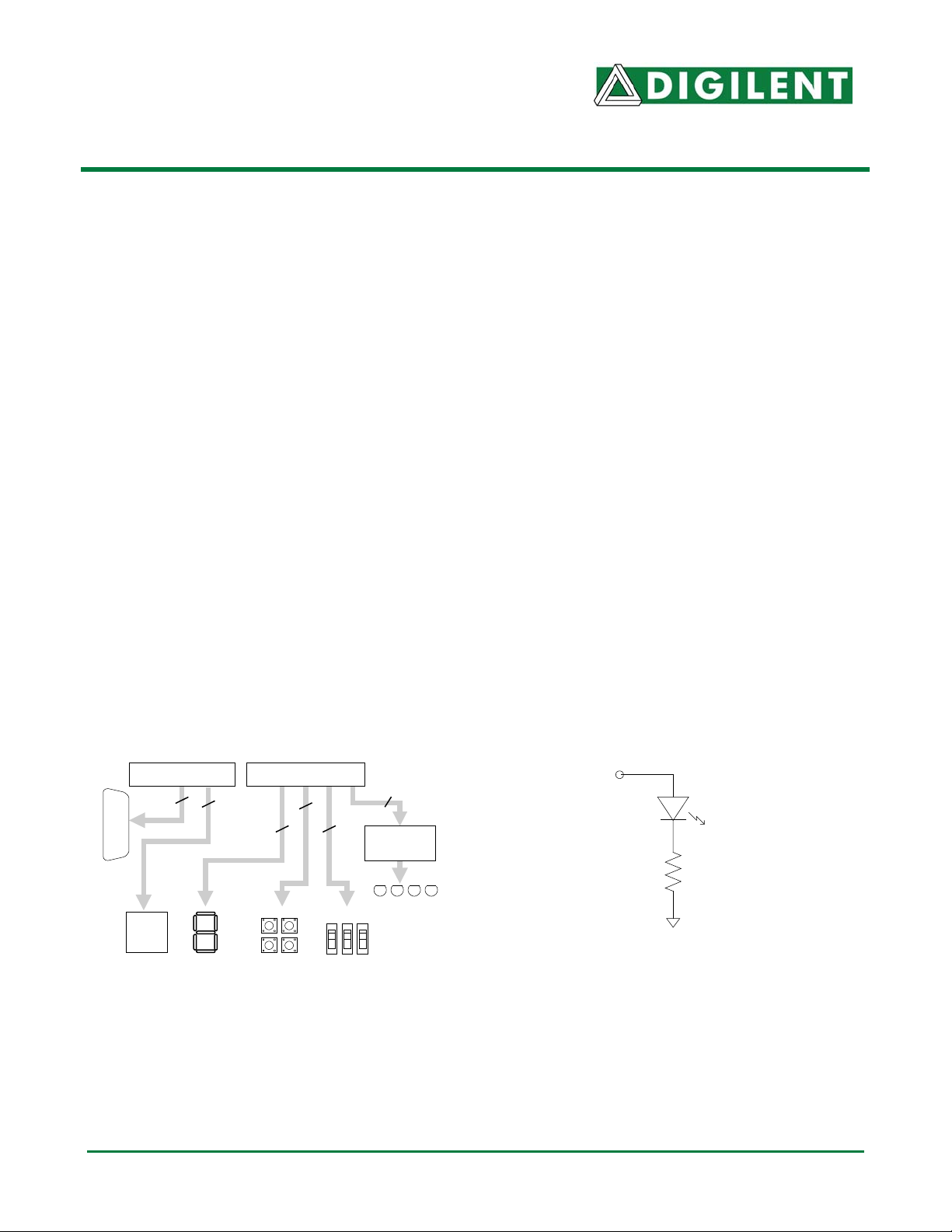
LEDs
Eight LEDs are provided for circuit outputs.
The LED cathodes are tied to ground via 270ohm resistors, and the anodes are driven from
the 74HC373 (so the LED drive signals are
active high).
®
Connector B
5
12
5 buttons
LD signals
9
8
74HC373
Latch
8 LEDs
Figure 2. LED Circuit
LD1- LD8
RP1
270 Ohm
GND
VGA Port
Connector A
5
2
PS2
port
4 displays 8 switches
Figure 1. DIO1 schematic
Signals
All named signals used on the DIO1 board are
defined in the Table 1. Voltage levels for all
Doc: 502-009 page 1 of 10
Copyright Digilent, Inc. All rights reserved. Other product and company names mentioned may be trademarks of their respective owners.
Page 2

Digilent DIO1 Reference Manual Digilent, Inc.
signals arriving from an attached Digilab
system board are determined by the system
board, but all signals arising on the I/O board
derive from the on-board 5VDC regulator (so
they are all 5V CMOS signals).
The DIO1 board uses a two-layer process, so
all signals are available on the top and bottom
layers. Many signals are brought to a test point
header for easy test and measurement
equipment attachment.
Power Supply
The DIO1 board receives system power from
pins 39 and 37 of connectors A and B (which
mate to pins 1 and 3 of an attached system
boards). Pin 37 provides Vdd from the attached
system board (assumed to be 3.3VDC), and pin
39 is connected to ground. Up to 5VDC can be
safely applied to the Vdd input pin (pin 37).
The DIO1 board typically consumes less than
10mA with no LED’s illuminated, and up to
130mA with all LEDs illuminated (including
Power Supplies
VU Unregulated power supply voltage from
attached system board – typically 59VDC. Although connected to the board,
this supply is not used on the DIO1
board.
VDD33 Regulated power supply voltage
(3.3VDC) from attached system board.
All devices on DIO1 board use this
supply.
GND System ground
VGA signals
HS VGA Horizontal Sync signal
VS VGA Vertical Sync signal
R VGA 1-bit red data
G VGA 1-bit green data
B VGA 1-bit blue data
PS2 signals
KCLK PS2 (Keyboard or Mouse) clock signal
KDAT PS2 (Keyboard or Mouse) data signal
Input devices
BTN1-4 Pushbuttons 1 through 4
SW1-
SW8
Output devices
LD0-LD8 Discreet LEDs 1 through 8
CA-CF Seven-segment display cathodes
AN1-
AN3
Table 1. DIO1 board signal definitions
Slide switches 1 through 8
Seven-segment display anodes
all segments of the seven-segment display).
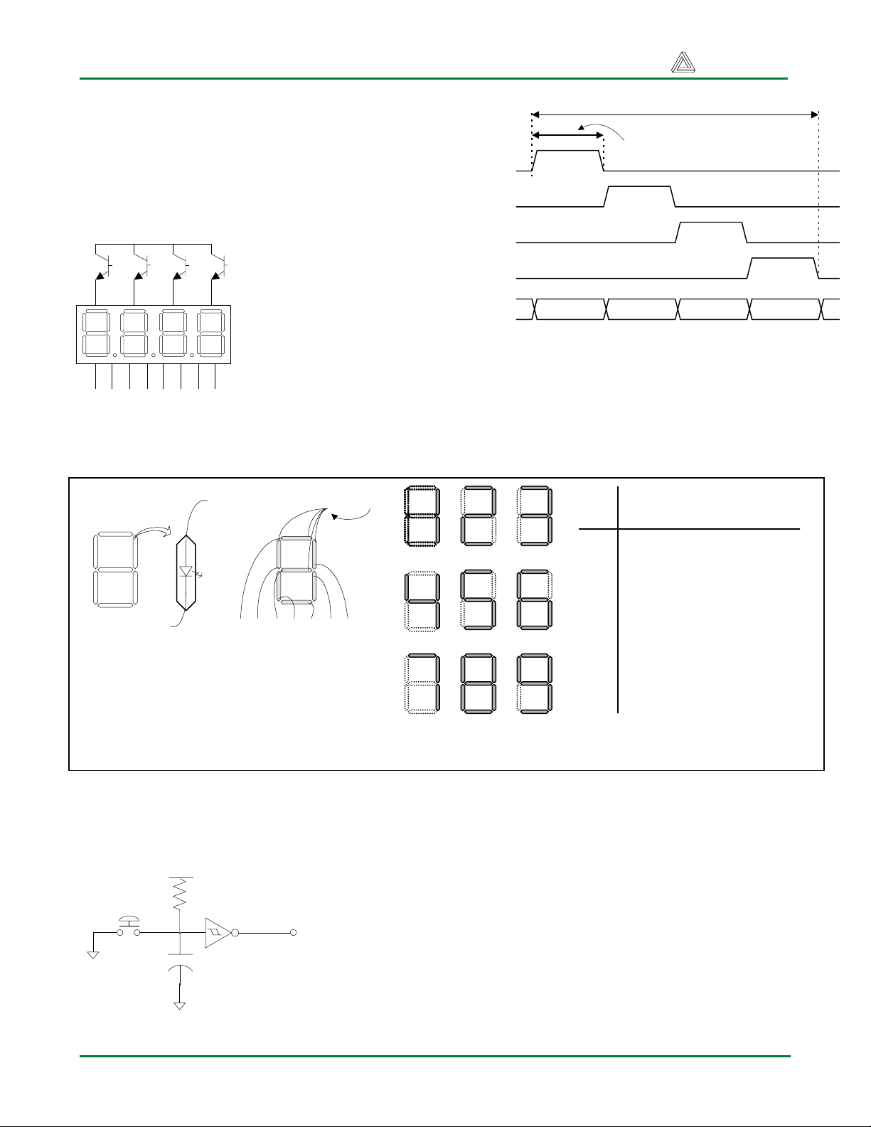
Seven-segment LED display
The DIO1 board contains a modular 4-digit,
common anode, seven-segment LED display.
In a common anode display, the seven anodes
of the LEDs forming each digit are connected
to four common circuit nodes (labeled AN1
through AN4 on the DIO1 board). Each anode,
and therefore each digit, can be independently
turned on and off by driving these signals to a
‘1’ or a ‘0’. The cathodes of similar segments
on all four displays are also connected together
into seven common circuit nodes labeled CA
through CG. Thus, each cathode for all four
displays can be turned on and off
independently.
This connection scheme creates a multiplexed
display, where driving the anode signals and
corresponding cathode patterns of each digit in
a repeating, continuous succession can create a
4-digit display. In order for each of the four
digits to appear bright and continuously
illuminated, all four digits should be driven
once every 1 to 16ms (for a refresh frequency
of 60Hz to 1KHz). For example, in a 60Hz
refresh scheme, each digit would be illuminated
for ¼ of the refresh cycle, or 4ms. The
controller must assure that the correct cathode
pattern is present when the corresponding
anode signal is driven. To illustrate the process,
if AN1 is driven high while CB and CC are
driven low, then a “1” will be displayed in digit
position 2. Then, if AN2 is driven high while
CA, CB and CC are driven low, then a “7” will
be displayed in digit position 2. If AN1/CB, CC
are driven for 4ms, and then AN2/CA, CB, CC
www.digilentinc.com page 2 of 10
Copyright Digilent, Inc. All rights reserved. Other product and company names mentioned may be trademarks of their respective owners.
Page 3
Digilent DIO1 Reference Manual Digilent, Inc.
are driven for 4ms in an endless succession, the
Refresh period = 1ms to 16ms
display will show “17” in the first two digits.
An example timing diagram is provided to the
right.
Anodes
via transistors for greater current
-- connected to CPLD
Vdd
a2
a3a4
a1
AN1
AN2
AN3
AN4
Digit period = Refresh / 4
Cathodes
Seven segment display refresh signals and timings
Digit 1 Digit 2 Digit 3 Digit 4
abcdefgdp
Cathodes
CPLD pins via 100
-- connected to
Ω
resistor
a
f
.
e
b
g
c
Common anode
d
(a) (b)
afgedcb
Figure 3. (a) Seven segm e nt display deta il.
(b) comm on a node display configuration. (c)
segement illumination patterns for decimal
digits. (d) segm e nt illum ination truth table.
VCC
4.7KOhm
To Connector
GND
.01uF
GND
Digit
Show
n
(c)
0
1
2
3
4
5
6
7
8
9
Illuminated Segment
a b c d e f g
1 1 1 1 1 1 0
0 1 1 0 0 0 0
1 1 0 1 1 0 1
1 1 1 1 0 0 1
0 1 1 0 0 1 1
1 0 1 1 0 1 1
1 0 1 1 1 1 1
1 1 1 0 0 0 0
1 1 1 1 1 1 1
1 1 1 1 0 1 1
(d)
Push Buttons
The 5 momentary-contact push buttons are
normally high when unused; this high signal is
translated to a low signal by a Schmitt Trigger.
When the button is actively pressed the signal
is driven low, which the Schmitt Trigger will
translate to a high signal. The buttons exhibit a
worst-case bounce time of about 1ms. A
74HC14 Hex Schmitt Trigger inverter provides
the debounce filtering and ESD protection. The
button outputs are brought out directly to pins
on interface connector B.
www.digilentinc.com page 3 of 10
Copyright Digilent, Inc. All rights reserved. Other product and company names mentioned may be trademarks of their respective owners.
Page 4

Digilent DIO1 Reference Manual Digilent, Inc.
Switches
The eight slide switches can be used to connect
either Vdd or GND to eight pins on interface
connecter B. The switches exhibit about 2ms of
bounce, and no active debouncing circuit is
employed. A 4.7K-ohm series resistor is used
for nominal input protection.
PS2 port
The DIO1 board includes a 6-pin
mini-DIN connector that can
accommodate a PS2 mouse or PS2
keyboard connection. Both the
2
4
6
mouse and keyboard use a twowire serial bus (including clock
and data) to communicate with a
host device, and both drive the bus
PS2 Connector front view
with identical signal timings. Both
use 11-bit words that include a start, stop and
odd parity bit, but the data packets are
organized differently, and the keyboard
interface allows bi-directional data transfers (so
1
5
Vdd
GND
RP6 & 7
4.7 KOhm
To
Connector
Pin 1
3
Pin 5Pin 6
Bottom-up
hole pattern
PS2 Pin Definitions
Pin Function
1 Data
2 Reserved
3 GND
4 Vdd
5 Clock
6 Reserved
state at logic ‘1’. The timings define signal
requirements for mouse-to-host
communications and bi-directional keyboard
communications.
the host device can illuminate state LEDs on
the keyboard).
Bus timings are shown below. The clock and
data signals are only driven when data transfers
occur, and otherwise they are held in the “idle”
T
T
CK
Symbol Parameter Min Max
T
Clock time
CK
T
Data-to-clock setup time
SU
T
Clock-to-data hold time 5us 25us
HLD
30us
5us
50us
25us
Edge 0
CLK
DATA
CK
T
T
SU
HLD
'1' stop bit'0' start bit
Edge 10
www.digilentinc.com page 4 of 10
Copyright Digilent, Inc. All rights reserved. Other product and company names mentioned may be trademarks of their respective owners.
Page 5

Digilent DIO1 Reference Manual Digilent, Inc.
Keyboard
The keyboard uses open collector drivers so
that either the keyboard or an attached host
device can drive the two-wire bus (if the host
device will not send data to the keyboard, then
the host can use simple input-only ports). The
clock and data signals (PS2C and PS2D) are
connected directly to pins on the B connector.
A PS2-style keyboard uses scan codes to
communicate key press data (nearly all
keyboards in use today are PS2 style). Each key
has a single, unique scan code that is sent
whenever the corresponding key is pressed. If
the key is pressed and held, the scan code will
be sent repeatedly once every 100ms or so.
When a key is released, a “F0” key-up code is
sent, followed by the scan code of the released
key. If a key has a “shift” character that is
A host device can also send data to the
keyboard. Below is a short list of some oftenused commands.
ED Turn on/off Num Lock, Caps Lock, and
Scroll Lock LEDs. The keyboard
acknowledges receipt of an “ED” by
returning an “FA”, after which the host
send another byte to set LED status: Bit 0
sets Scroll Lock; bit 1 sets the Num Lock;
and Bit 2 sets Caps lock. Bits 3 to 7 are
ignored.
EE Echo. Upon receiving an echo command,
the keyboard replies with the same scan
code (“EE”).
F3 Set scan code repeat rate. The keyboard
acknowledges receipt of an “F3” by
returning an “FA”, after which the host
sends a second byte to set the repeat rate.
FE Resend. Upon receiving a resend
ESC
76
` ~
0E
TAB
0D
Caps Lock
58
Shift
12
Ctrl
14
F105F206F304F4
0C
1 !162 @1E3 #264 $255 %
2E
Q
15W1DE24R2DT2C
A
1CS1BD23F2BG34
Z
1ZX22C21V2AB32
Alt
11
F503F60BF783F8
6 ^367 &3D8 *3E9 (460 )45- _4E= +55BackSpace
Y
35U3CI43O44P4D
H
33J3BK42L4B
Space
29
different than the non-shift character, the same
scan code is sent whether the shift key is
pressed or not, and the host device must
determine which character to use. Some keys,
called extended keys, send an “E0” ahead of
the scan code (and they may send more than
one scan code). When an extended key is
released, an “E0 F0” key-up code is sent,
followed by the scan code. Scan codes for most
keys are shown in the figure below.
N
31M3A
F901F1009F1178F12
0A
; :
4C
, <41> .49/ ?
4A
Alt
E0 11
[ {54] }
5B
' "
52
Enter
Shift
59
66
\ |
5D
5A
Ctrl
E0 14
07
E0 75
E0 74
E0 6B
E0 72
command, the keyboard will re-send the
last scan code sent.
FF Reset. Resets the keyboard.
The keyboard should send data to the host only
when both the data and clock lines are high (or
idle). Since the host is the “bus master”, the
keyboard should check to see whether the host
is sending data before driving the bus. To
facilitate this, the clock line can be used as a
“clear to send” signal. If the host pulls the
clock line low, the keyboard must not send any
data until the clock is released (host-to-
www.digilentinc.com page 5 of 10
Copyright Digilent, Inc. All rights reserved. Other product and company names mentioned may be trademarks of their respective owners.
Page 6
Digilent DIO1 Reference Manual Digilent, Inc.
keyboard data transmission will not be dealt
with further here).
The keyboard sends data to the host in 11-bit
words that contain a ‘0’ start bit, followed by 8bits of scan code (LSB first), followed by an
odd parity bit and terminated with a ‘1’ stop
bit. The keyboard generates 11 clock transitions
(at around 20 - 30KHz) when the data is sent,
and data is valid on the falling edge of the
clock.
1 indicates a negative number). The magnitude
of the X and Y numbers represent the rate of
mouse movement – the larger the number, the
faster the mouse is moving (the XV and YV
bits in the status byte are movement overflow
indicators – a ‘1’ means overflow has
occurred). If the mouse moves continuously,
the 33-bit transmissions are repeated every
50ms or so. The L and R fields in the status
byte indicate Left and Right button presses (a
‘1’ indicates the button is being pressed).
Mouse
The mouse outputs a clock and data signal
when it is moved; otherwise, these signals
remain at logic ‘1’. Each time the mouse is
moved, three 11-bit words are sent from the
mouse to the host device. Each of the 11-bit
words contains a ‘0’ start bit, followed by 8 bits
of data (LSB first), followed by an odd parity
bit, and terminated with a ‘1’ stop bit. Thus,
each data transmission contains 33 bits, where
bits 0, 11, and 22 are ‘0’ start bits, and bits 10,
21, and 32 are ‘1’ stop bits. The three 8-bit data
fields contain movement data as shown below.
Mouse status byte X direction byte Y direction byte
L R 0 1 XS YS XY YY P X0 X1 X2 X3 X4 X5 X6 X7 P Y0 Y1 Y2 Y3 Y4 Y5 Y6 Y7 P
10 100 11
Idle state
Start bit Stop bit
Start bit
Stop bit
Start bit
Stop bit
Idle state
Data is valid at the falling edge of the clock,
and the clock period is 20 to 30KHz.
The mouse assumes a relative coordinate
system wherein moving the mouse to the right
generates a positive number in the X field, and
moving to the left generates a negative number.
Likewise, moving the mouse up generates a
positive number in the Y field, and moving
down represents a negative number (the XS and
YS bits in the status byte are the sign bits – a 1’
www.digilentinc.com page 6 of 10
Copyright Digilent, Inc. All rights reserved. Other product and company names mentioned may be trademarks of their respective owners.
Page 7

Digilent DIO1 Reference Manual Digilent, Inc.
VGA port
The five standard VGA signals Red (R), Green
(G), Blue (B), Horizontal Sync (HS), and
Vertical Sync (VS) are routed directly from the
A connector to the VGA connector. A series
resistor is used on each color line to provide 3bit color, with 1 bit each for Red, Green, and
Blue. The series resistor uses the 75 ohm VGA
cable termination to ensure that the color
signals remain in the VGA-specified 0V – 0.7V
range. The HS and VS signals are TTL level.
VGA signal timings are specified, published,
copyrighted and sold by the VESA
organization (www.vesa.org). The following
VGA system and timing information is
provided as an example of how a VGA monitor
might be driven in 640 by 480 mode. For more
precise information, or for information on
higher VGA frequencies, refer to document
available at the VESA website (or
experiment!).
Pin 5
Pin 10
Pin 15
DB15 VGA connector
Front view
DB15
Connector
1
6
11
2
7
12
3
8
13
4
9
14
5
10
15
Pin 1
Pin 6
Pin 11
Red
Green
Blue
Horizontal Sync
Vertical Sync
Pin 1
Pin 15
DB15 through-hole pattern as
seen from the top
470
To R on Connector B
470
To G on Connector B
470
To B on Connector B
To HS on Connector B
To VS on Connector B
GND
www.digilentinc.com page 7 of 10
Copyright Digilent, Inc. All rights reserved. Other product and company names mentioned may be trademarks of their respective owners.
VGA systems and signal timings for a 60Hz,
640x480 display
Page 8

Digilent DIO1 Reference Manual Digilent, Inc.
CRT-based VGA displays use amplitude
modulated, moving electron beams (or cathode
rays) to display information on a phosphorcoated screen. LCD displays use an array of
switches that can impose a voltage across a
small amount of liquid crystal, thereby
changing light permittivity through the crystal
on a pixel-by-pixel basis. Although the
following description is limited to CRT
displays, LCD displays have evolved to use the
same signal timings as CRT displays (so the
“signals” discussion below pertains to both
CRTs and LCDs).
CRT displays use electron beams (one for red,
one for blue and one for green) to illuminate
phosphor that coats the inner side of the display
end of a cathode ray tube (see drawing below).
Electron beams emanate from “electron guns”,
where two coils of wire produce orthogonal
electromagnetic fields. Because cathode rays
are composed of charged particles (electrons),
they can be bent by these magnetic fields.
Current waveforms are passed through the coils
to produce magnetic fields that cause the
electron beams to transverse the display surface
in a “raster” pattern, horizontally from left to
right and vertically from top to bottom.
Information is only displayed when the beam is
moving in the “forward” direction (left to right
and top to bottom), and not during the time the
beam is reset back to the left or top edge of the
display. Much of the potential display time is
therefore lost in “blanking” periods when the
beam is reset and stabilized to begin a new
horizontal or vertical display pass.
The size of the beams, the frequency at which
the beam can be traced across the display, and
which are a finely pointed, heated
cathodes placed in close proximity to
a positively charged annular plate
called a “grid”. The electrostatic force
imposed by the grid pulls away rays
of energized electrons as current
flows into the cathodes. These particle
Anode (entire screen)
Cathode ray
Cathode ray tube
Deflection coils
Grid
Electron guns
(Red, Blue, Green)
rays are initially accelerated towards
the grid, but they soon fall under the
influence of the much larger
electrostatic force that results from
the entire phosphor coated display
surface of the CRT being charged to
20kV (or more). The rays are focused
High voltage supply
(>20kV)
deflection
control
grid
control
Control board
gun
control
Sync signals
(to deflection control)
R,G,B signals (to guns)
to a fine beam as they pass through
the center of the grids, and then they
accelerate to impact on the phosphor
coated display surface. The phosphor surface
glows brightly at the impact point, and the
phosphor continues to glow for several hundred
microseconds after the beam is removed. The
larger the current fed into the cathode, the
brighter the phosphor will glow.
Between the grid and the display surface, the
beam passes through the neck of the CRT
the frequency at which the electron beam can
be modulated determine the display resolution.
Modern VGA displays can accommodate
different resolutions, and a VGA controller
circuit dictates the resolution by producing
timing signals to control the raster patterns. The
controller must produce TTL-level
synchronizing pulses to set the frequency at
which current flows through the deflection
coils, and it must ensure that pixel (or video)
Cathode ray tube display system
VGA cable
www.digilentinc.com page 8 of 10
Copyright Digilent, Inc. All rights reserved. Other product and company names mentioned may be trademarks of their respective owners.
Page 9

Digilent DIO1 Reference Manual Digilent, Inc.
o
Symbol Parameter
T
Sync pulse time
S
T
disp
T
pw
T
fp
T
bp
Display time
VS pulse width
VS front porch
VS back porch
Vertical Sync
Time Clocks Lines
16.7ms
15.36ms
320 us
928 us
64 us
416,800
384,000
1,600
8,000
23,200
521
480
2
10
29
data is applied to the
electron guns at the correct
time. Video data typically
comes from a video refresh
memory; with one or more
bytes assigned to each pixel
location (the DIO1 board
uses 3-bits per pixel). The
controller must index into
video memory as the beams
move across the display,
and retrieve and apply
video data to the display at
Current
through
horizontal
defletion
coil
precisely the time the
electron beam is moving
across a given pixel.
The VGA controller circuit
must generate the HS and
VS timings signals and
coordinate the delivery of
time
video data based on the
pixel clock. The pixel clock
HS
defines the time available
to display 1 pixel of
information. The VS signal
defines the “refresh”
frequency of the display, or the frequency at
which all information on the display is
redrawn. The minimum refresh frequency is a
function of the display’s phosphor and electron
beam intensity, with practical refresh
frequencies falling in the 60Hz to 120Hz range.
The number of lines to be displayed at a given
refresh frequency defines the horizontal
“retrace”
Horizont al Sync
Time
25.6 us
3.84 us
640 ns
1.92 us
Clocks
32 us
pixel 0,0
800
640
96
16
48
640 pixels are displayed each time
the beam travels across the screen
VGA display
surface
pixel 479,0 pixel 479,639
Stable current ramp - information
displayed during this time
Total horizontal time
Horizontal display time
Horizontal sync signal
sets retrace frequency
VGA Signal Timing
A VGA controller circuit decodes the output of
a horizontal-sync counter driven by the pixel
clock to generate HS signal timings. This
counter can be used to locate any pixel location
on a given row. Likewise, the output of a
vertical-sync counter that increments with each
HS pulse can be used to generate VS signal
timings, and this counter can be used to locate
T
pw
pixel 0,639
T
S
T
disp
retrace time
"back porch""front porch"
T
T
bp
Retrace - n
information
displayed
during this
time
fp
www.digilentinc.com page 9 of 10
Copyright Digilent, Inc. All rights reserved. Other product and company names mentioned may be trademarks of their respective owners.
Page 10

Digilent DIO1 Reference Manual Digilent, Inc.
any given row. These two continually running
counters can be used to form an address into
video RAM. No time relationship between the
onset of the HS pulse and the onset of the VS
pulse is specified, so the designer can arrange
the counters to easily form video RAM
addresses, or to minimize decoding logic for
Connector pinouts
The connector pinouts are shown below.
Separately available tables show pass-through
connections for the devices on the DIO1 board
when the board is attached to various system
boards – i.e., one table is available showing the
FPGA connections to the DIO1 devices for a
D2 system board, another table is available
showing the FPGA connections for a D2E
board, a third for the D2XL board, etc.
sync pulse generation.
J2 (B) connector
Pin Signal Pin Signal Pin Signal Pin Signal
1 CA 11 CF 21 A1 31 n/c 30 BLU
2 SW1 12 SW6 22 LD1 32 LD6 32 PS2D
3 CB 13 CG 23 A2 33 n/c 33 GRN
4 SW2 14 SW7 24 LD2 34 LD7 34 PS2C
5 CC 15 DP 25 A3 35 n/c 35 RED
6 SW3 16 SW8 26 LD3 36 LD8 36 HS
7 CD 17 BTN2 27 A4 37 VDD33 37 VDD
8 SW4 18 BTN1 28 LD4 38 LDG 38 VS
9 CE 19 BTN4 29 n/c 39 GND 39 GND
10 SW5 20 BTN3 30 LD5 40 VU
J1 (A) Connector
Pin Signal
40 VU
www.digilentinc.com page 10 of 10
Copyright Digilent, Inc. All rights reserved. Other product and company names mentioned may be trademarks of their respective owners.
 Loading...