

Page 1
DDiiggiilleenntt DDiiggiillaabb 22
RReeffeerreennccee MMaannuuaal
Revision: 5/7/02 215 E Main Suite D | Pullman, WA 99163
l
www.digilentinc.com
(509) 334 6306 Voice and Fax
Overview
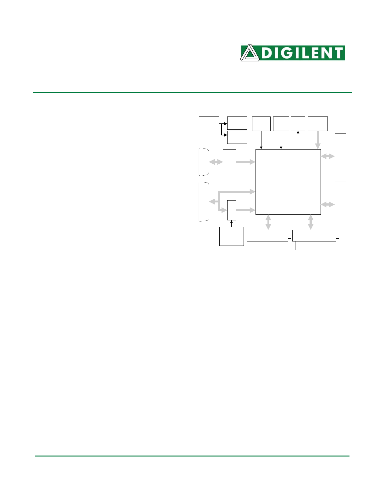
The Digilab 2 development board (the D2)
features the Xilinx Spartan 2 XC2S200 FPGA
circuit board and provides an inexpensive and
expandable platform on which to design and
implement digital circuits of all kinds. D2
board features include:
Power
jack
5-9VDC
Serial PortParallel Port
2.5VDC
regulator
3.3VDC
regulator
Serial
Port
RS-232
converter
EPP or SPP
parallel port
50MHz
CLK
Push
button
Xilinx Spartan2
XC2S200-PQ208
Status
LED
SPROM
• A Xilinx XC2S200 FPGA;
Buffer
JTAG
Port
Expansion C Expansion D
• Dual on-board 1.5A power regulators
(2.5V and 3.3V);
• A socketed 50MHz oscillator;
• An EPP-capable parallel port for JTAG-
based FPGA programming and user data
transfers;
• A 5-wire Rs-232 serial port;
• A status LED and pushbutton for basic
I/O;
Port/prog
control
switch
Expansion A Expansion B
Expansion E Expansion F
D2 circuit board block diagram
• Six 100-mil spaced, right-angle DIP
socket 40-pin expansion connectors.
The D2 board has been designed specifically to
work with Xilinx ISE CAD tools, including the
free WebPack tools available from the Xilinx
website. Like other Spartan 2 boards in the
Digilab family, the D2 board has been
partitioned so that only the hardware required
for a particular project need be purchased.
Several existing peripheral boards that mate
with the expansion connectors are currently
available (see www.digilentinc.com), and new
boards are frequently added. The low-cost,
standard expansion connectors allow new
peripheral boards, including wire-wrap or
manually soldered boards, to be quickly
designed and used. The D2 board ships with a
power supply and programming cable, so
designs can be implemented immediately
without the need for any additional hardware.
Functional description
The Digilab D2 board has been designed to offer an unembellished, low-cost system for designers who
need a flexible platform to gain exposure to the Spartan 2 device, or for those who need to rapidly
prototype FPGA-based designs. The D2 board provides only the essential supporting devices for the
Spartan 2, and routes all available FPGA signals to standard expansion connectors. Included on the
board are 2.5VDC and 3.3VDC regulators, a JTAG configuration circuit that uses a standard parallel
®
Doc: 502-004 page 1 of 10
Copyright Digilent, Inc. All rights reserved. Other product and company names mentioned may be trademarks of their respective owners.
Page 2
Digilent Digilab 2 Reference Manual Digilent, Inc.
cable, basic communication ports including an enhanced parallel port and 5-wire serial port, a 50MHz
oscillator, and a pushbutton and LED for rudimentary I/O.
The D2 board has been designed
to serve as a host for various
peripheral boards. The expansion
connectors on the D2 board mate
with standard 40-pin, 100 mil
spaced DIP headers available
from any catalog distributor.
Expansion connectors provide the
unregulated supply voltage (VU),
3.3V, GND, and 37 FPGA
signals to peripheral boards, so
system designers can quickly
develop application-specific
peripheral boards. Digilent also
produces an assortment of other
expansion boards featuring
commonly used devices. Visit the
Digilent website for a listing of
currently available boards.
(www.digilentinc.com)
Table 1 shows all signals routed
on the D2 board. These signals,
and the circuits to which they
connect, are described in the
following sections.
Power Supplies
VU Unregulated power supply voltage – depends on power
supply used. Must be between 5VDC and 10VDC. Routed to
regulators and expansion connectors only.
VDD33 VCCO/VCC for all devices, routed on PCB plane. 1.5A can
be drawn with less than 20mV ripple (typical)
VDD25 FPGA VCCINT routed on PCB plane
GND System ground routed to all devices on PCB ground plane
Programming and parallel port
PWE EPP mode write enable sign al (in to FPGA)
PD0-PD7 Bi-directional data signals
PINT Interrupt signal (out from FPGA)
PWT EPP mode wait signal (out from FPGA)
PDS EPP mode data strobe (in to FPGA)
PRS Reset signal (in to FPGA)
PAS EPP mode address strobe (in to FPGA)
Serial port
RXD Serial port receive data (in to FPGA)
TXD Serial port send data (out from FPGA)
DSR Serial port data set ready (out from FPGA)
CTS Serial port clear to send (out from FPGA)
RST Serial port request to send (in to FPGA)
On board devices
BTN1 User-controllable pushbutton input
LED1 User-controllable status LED
CLK1 CMOS oscillator connected to GCLK0
Expansion Connectors
A4-A40 A bus signals connecting the A & E connectors to the FPGA
B4-B14 B bus signals connecting the B & F connectors to the FPGA
C4-C40 C bus signals connecting the C connector to the FPGA
D4-D40 D bus signals connecting the D connector to the FPGA
Table 1. D2 board signal definitions
Parallel port and FPGA configuration circuit
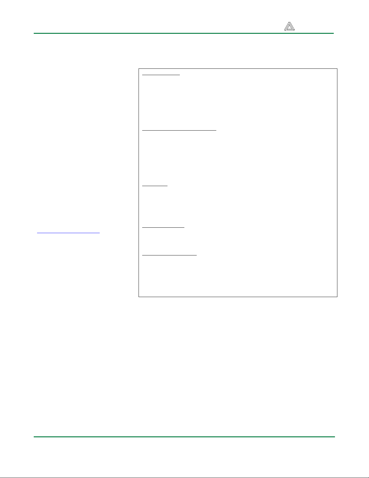
The Digilab 2 board uses a DB-25 parallel port connector to route JTAG programming signals from a
host computer to the FPGA. This same connector also routes the computer’s parallel port pins to the
FPGA following the EPP port definition contained in the IEEE 1284 standard. A three-state buffer,
controlled by a switch, determines whether the JTAG port or EPP port is enabled. With this circuit, the
FPGA can be configured using the JTAG protocol over the parallel cable. The same cable can then be
used (after the switch is repositioned) to move data between the board and the host computer using the
high-speed EPP protocol. A separate JTAG header is also provided so that a dedicated programming
cable (like the Xilinx Parallel III cable) can be used.
The JTAG programming circuit follows the JTAG schematic available from Xilinx, so that the Digilab
2 board is fully compatible with all Xilinx programming tools. The EPP parallel port circuit follows
IEEE 1284 specification guidelines, and data rates approaching 2Mbytes/second can be achieved.
JTAG and EPP connections are shown in the diagrams (Figure 1) below.
www.digilentinc.com page 2 of 10
Copyright Digilent, Inc. All rights reserved. Other product and company names mentioned may be trademarks of their respective owners.
Page 3
Digilent Digilab 2 Reference Manual Digilent, Inc.
Pin 13 Pin 1
Pin 25
DB25 parallel port connector
Front view
Pin 25
Top view of hole pattern, with
cable attaching from this side
Pin 14
Pin 1
Pin EPP signal EPP Function
1 Write Enable (O) Low for read, High for write
2-9 Data bus (B) Bi-directional data lines
10 Interrupt (I) Interrupt/acknowledge input
11 Wait (I) Bus handshake; low to ack
12 Spare NOT CONNECTED
13 Spare NOT CONNECTED
14 Data Strobe (O) Low when data valid
15 Spare NOT CONNECTED
16 Reset (O) Low to reset
17 Address strobe (O) Low when address valid
18-25 GND System ground
Figure 1. Parallel port connectors and signals
The D2 board directly supports JTAG and SPROM configuration. Hardware debugger configuration is
supported indirectly. To configure the board from a computer using the JTAG mode, set switch 1
(SW1) in the JTAG position, and attach a power supply and programming cable. The power supply
must be connected before the parallel cable or the board may hang in a non-communicating state. The
board will be auto-detected by the Xilinx JTAG programming software, and all normal JTAG
operations will be available.
To configure the FPGA from an SPROM, load the programmed SPROM into the 8-pin ROM socket
(labeled IC6), place SW1 in the PORT position, add jumpers to all mode pins, and apply power.
To configure the board using the hardware debugger protocol, a slight board modification is required –
a jumper wire must be soldered to the non-VCC side of R45. Insert wire-wrap posts into the SPROM
socket, attach the hardware debugger signals to the appropriate posts, and attach the PROG signal to
the jumper wire attached to R45. The hardware debugger programming software will now
automatically recognize the board and hardware debugger programming can proceed as normal.
Programming circuit detail is shown below (Figure 2). Note that all parallel port signals are routed to
the test header J12 for easy connection of test and measurement equipment.
www.digilentinc.com page 3 of 10
Copyright Digilent, Inc. All rights reserved. Other product and company names mentioned may be trademarks of their respective owners.
Page 4

Digilent Digilab 2 Reference Manual Digilent, Inc.
1
14
2
15
3
16
4
17
5
18
6
19
7
20
8
21
9
22
10
23
11
24
12
25
13
DB25
connector
Pull-up resistors are used on all parallel
port signals. They are not shown here.
GND
Write Enable (PWE)
Data Strobe (PDS)
Data 0 (PD0)
Data 1 (PD1)
Reset (PRST)
Data 2 (PD2)
Address Strobe (PAS)
Data 3 (PD3)
Data 4 (PD4)
Data 5 (PD5)
Data 6 (PD6)
Data 7 (PD7)
Interrupt (PINT)
Wait (PWT)
P206
P205
P15
P14
P203
P10
P204
P9
Xilinx
P8
Spartan 2E
PQ208
P7
P6
P5
P4
P3 P2
VDD SENSE
CABLE DET1
CABLE DET2
P107
P155
P153
P104
P157
P207
P159
Pull-ups on INIT and
DONE not shown
INIT
CCLK
DATA IN
DONE
M0
M1
M2
Jumper
block
TDO
TCLK
TDI
TMS
SPROM
8-DIP
Decouping
PORT
Vdd
three-state
buffer
Enable
Program enable
GND
switch (SW1)
JTAG
Figure 2. Parallel port and programming circuit schematic
Serial Port
The D2 serial port uses a Maxim MAX3386E RS-232 voltage converter to generate the required RS232 voltages. Five signals are connected through the RS-232 converter, allowing for partial hardware
handshaking. The serial port pin definitions and circuit are shown in Figure 3. The serial port is
provided, in part, to support the Xilinx MicroBlaze embedded RSIC processor core available from the
Xilinx website.
The two devices connected to either end of a serial cable are designated as the Data Terminal
Equipment (DTE) and the Data Communications Equipment (DCE). The DCE was originally
conceived to be a modem, but now many devices connect to a computer as a DCE. A DTE device uses
a male DB-9 connector, and a DCE device uses a female DB-9 connector. The DTE is considered the
www.digilentinc.com page 4 of 10
Copyright Digilent, Inc. All rights reserved. Other product and company names mentioned may be trademarks of their respective owners.
Page 5

Digilent Digilab 2 Reference Manual Digilent, Inc.
source of data, and the DCE the peripheral device. Two DTE devices can be connected via a serial
cable, only if lines two and three are crossed – this is referred to as a null modem cable. A DTE and
DCE device can be connected with a straight-through cable. The Digilab 2 board is configured as a
DCE device.
Serial Port Pin Definitions
Pin # Name Function Direction Connected
Pin 1Pin 9
DB9 top-down
hole pattern; cable
attaches from this side
Pin 5
Pin 9
DB9 serial port connector
Front view
Pin 1
Pin 6
1 DCD Data carrier detect DCE DTE N
2 RXD Received data DCE DTE Y
3 TXD Transmitted data DCE DTE Y
4 DTR Data terminal ready DCE DTE N
5 SG Signal ground Y
6 DSR Data set ready DCE DTE Y
7 RTS Request to send DCE DTE Y
8 CTS Clear to send DCE DTE Y
9 RI Ring Indicator DCE DTE N
1
GND
DSR
RXD
RTS
TXD
CTS
16
17
13
14
15
Maxim
MAX3386E
RS232 Voltage
Converter
10
11
8
7
9
P200
P202
P195
P201
P199
Xilinx
Spartan 2
PQ208
6
2
7
3
8
4
9
5
DB9
Connector
Figure 3. Serial port circuit schematic
Oscillator
The Digilab 2 uses a socketed half-size 8-pin DIP oscillator. The board ships with a 50MHz oscillator,
allowing for system clocks ranging from DC to 200MHz (using the Spartan 2 DLL circuit and/or clock
counter-dividers). Oscillators from 32KHz to 100MHz can easily be substituted, allowing for a wide
range of clock frequencies. The oscillator, which is connected to the FPGA GCK0 input (P80), is
bypassed with a 0.1uF capacitor and it is physically located as close to the FPGA as possible (trace
length is about 10mm).
Power Supplies
The Digilab 2 board uses two LM317 1.5A voltage regulators to produce 2.5VDC and 3.3VDC
supplies. The regulator inputs are driven from an external DC power supply connected to the on-board
2.1mm center-positive power jack. The regulators have 10uF of input capacitance, 20uF of local output
capacitance, and 10uF of regulation bypass capacitance. This allows the regulators to produce stable,
www.digilentinc.com page 5 of 10
Copyright Digilent, Inc. All rights reserved. Other product and company names mentioned may be trademarks of their respective owners.
Page 6

Digilent Digilab 2 Reference Manual Digilent, Inc.
low noise supplies using inexpensive power supplies, regardless of load (up to 1.5A). The regulator
bodies are soldered to the board for improved thermal dissipation. DC supplies in the range of 5VDC
to 10VDC may be used.
The Digilab 2 board uses a four layer PCB, with the inner layers dedicated to VCC and GND planes.
Most of the VCC plane is at 3.3V, with an island under the FPGA at 2.5V. The FPGA and the other
ICs on the board all have 0.1uF bypass capacitors placed as close as possible to the VCC pins.
Total board current is dependent on FPGA configuration, clock frequency, and external connections. In
test circuits with roughly 50K gates routed, a 50MHz clock source and a single expansion board
attached (the DIO2 board), approximately 200mA +/- 30% of supply current is drawn from the 2.5V
supply and approximately 150mA +/- 50% is drawn from the 3.3V supply. These currents are strongly
dependent on FPGA and peripheral board configurations.
All FPGA VCCO pins are connected to the 3.3V supply. If other VCCO voltages are required, please
contact Digilent for information regarding various options (www.digilentinc.com).
Expansion connectors
Pin 39
Pin 40
Pin 3: 3.3V
Pin 4
Pin 1: GND
Pin 2: VU
Pin 39
Pin 40
The six expansion connectors, shown in Figure 4,
are labeled A-F and use 100 mil spaced DIP headers.
A
B
All six connectors have GND routed to pin 1, VU
routed to pin 2, and 3.3V routed to pin 3. Pins 4-40
all route directly to the FPGA. The connectors are
organized in pairs, with the A & B, C& D, and E &
DB-9
C
F pairs placed on the same board edge. Connectors
A & B and E & F are routed in parallel, with pairs A
37
& E and B & F sharing identical pin connections to
9
the FPGA. Connectors C & D have all pins routed to
separate FPGA pins. All connector pairs are
separated by 400 mils, so any peripheral board can
be placed in any connector (or pair of connectors).
DB-25
Spartan 2
PQ208
37
37
D
The PQ208 package used on the D2 board allows
122 signals to be routed to the expansion connectors
(the remaining 21 available signals are routed to the
parallel and serial connectors). Connectors C & D
are closest to the FPGA, and all C & D pins are
FE
Figure 4. Expansion connector detail
connected to the closest available FPGA pins with
the shortest possible route. Thus, the 74 FPGA signals routed to the C & D connectors will exhibit the
www.digilentinc.com page 6 of 10
Copyright Digilent, Inc. All rights reserved. Other product and company names mentioned may be trademarks of their respective owners.
Page 7

Digilent Digilab 2 Reference Manual Digilent, Inc.
least amount of signal delay, and data rates of up to 100MHz are attainable. The A & E connectors also
route 37 FPGA signals, but along less favorable routes. Only 9 FPGA signals were left to route to the
B & F connectors, so 28 pins on those connectors are not attached to anything. Connector pin
definitions are shown in Table 2.
www.digilentinc.com page 7 of 10
Copyright Digilent, Inc. All rights reserved. Other product and company names mentioned may be trademarks of their respective owners.
Page 8

Digilent Digilab 2 Reference Manual Digilent, Inc.
Table 2. Digilab 2 Expansion Connector pinouts
A&E connector B&F connector C connector D connector
Pin Signal S-II pin Pin Signal S-II pin Pin Signal S-II pin Pin Signal S-II pin
1 GND - 1 GND - 1 GND - 1 GND 2 VU - 2 VU - 2 VU - 2 VU 3 VDD33 - 3 VDD33 - 3 VDD33 - 3 VDD33 4 A4 70 4 B4 194 4 C4 181 4 D4 127
5 A5 69 5 B5 193 5 C5 180 5 D5 125
6 A6 68 6 B6 192 6 C6 179 6 D6 126
7 A7 67 7 B7 191 7 C7 178 7 D7 122
8 A8 63 8 B8 189 8 C8 176 8 D8 123
9 A9 62 9 B9 188 9 C9 175 9 D9 120
10 A10 61 10 B10 187 10 C10 174 10 D10 121
11 A11 60 11 B11 185* 11 C11 173 11 D11 115
12 A12 59 12 B12 182* 12 C12 172 12 D12 119
13 A13 58 13 B13 - 13 C13 168 13 D13 113
14 A14 57 14 B14 - 14 C14 167 14 D14 114
15 A15 49 15 B15 - 15 C15 166 15 D15 111
16 A16 48 16 B16 - 16 C16 165 16 D16 112
17 A17 47 17 B17 - 17 C17 164 17 D17 109
18 A18 46 18 NC - 18 C18 163 18 D18 110
19 A19 45 19 NC - 19 C19 162 19 D19 102
20 A20 44 20 NC - 20 C20 161 20 D20 108
21 A21 43 21 NC - 21 C21 160 21 D21 100
22 A22 42 22 NC - 22 C22 154 22 D22 101
23 A23 41 23 NC - 23 C23 152 23 D23 98
24 A24 37 24 NC - 24 C24 151 24 D24 99
25 A25 36 25 NC - 25 C25 150 25 D25 96
26 A26 35 26 NC - 26 C26 149 26 D26 97
27 A27 34 27 NC - 27 C27 148 27 D27 94
28 A28 33 28 NC - 28 C28 147 28 D28 95
29 A29 31 29 NC - 29 C29 146 29 D29 89
30 A30 30 30 NC - 30 C30 142 30 D30 90
31 A31 29 31 NC - 31 C31 141 31 D31 87
32 A32 27 32 NC - 32 C32 140 32 D32 88
33 A33 24 33 NC - 33 C33 139 33 D33 84
34 A34 23 34 NC - 34 C34 138 34 D34 86
35 A35 22 35 NC - 35 C35 136 35 D35 82
36 A36 21 36 NC - 36 C36 135 36 D36 83
37 A37 20 37 NC - 37 C37 134 37 D37 75
38 A38 18 38 NC - 38 C38 133 38 D38 81
39 A39 17 39 NC - 39 C39 132 39 D39 73
40 A40 16 40 NC - 40 C40 129 40 D40 74
* uses GCLK pin
www.digilentinc.com page 8 of 10
Copyright Digilent, Inc. All rights reserved. Other product and company names mentioned may be trademarks of their respective owners.
Page 9
Digilent Digilab 2 Reference Manual Digilent, Inc.
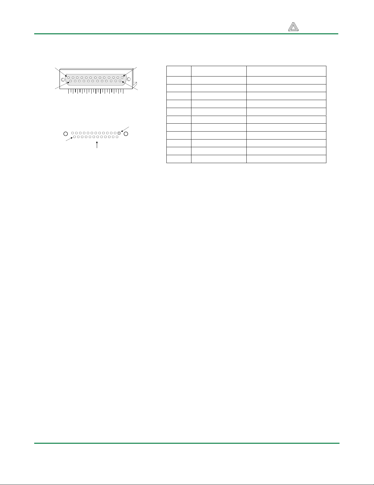
Pushbutton and LED
A single pushbutton and LED are provided on the board, allowing basic status and control functions to
be implemented without a peripheral board. For example, the LED can be illuminated from a signal in
the FPGA to verify that configuration has been successful, and the pushbutton can be used to provide a
basic reset function independent of other inputs. The circuits are shown in Figure 5, below.
Vdd
P77
4.7K
4.7K
Xilinx
Spartan 2
PQ208
80 Ohm
P71
Push
button
Figure 5. Pushbutton and LED detail
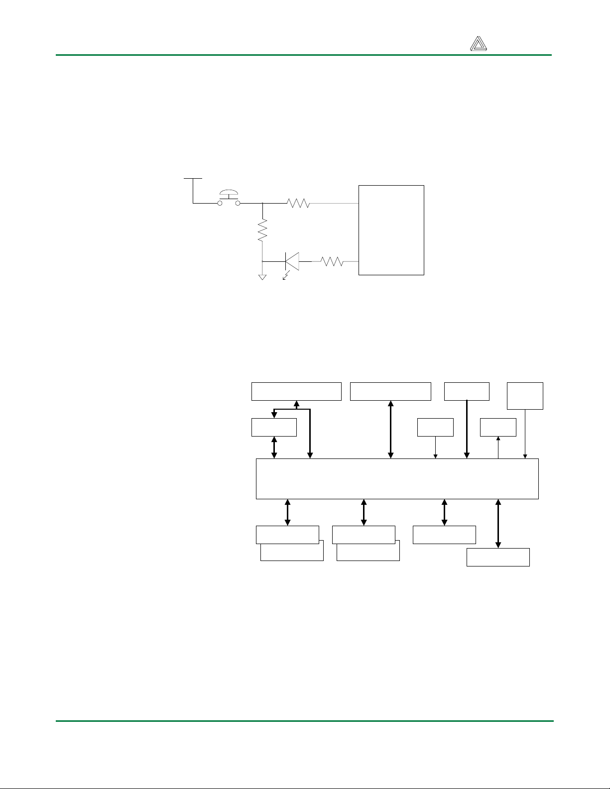
Spartan 2 FPGA
The block diagram of the Digilab 2
board (Page 1) shows all
connections between the FPGA and
the devices on the board. All FPGA
pin connections are shown in Table
3 (below).
DB-25 parallel port DB-9 serial port
54
JTAG
13
4
SPROM
Clock
Push
button
LED
The Spartan device, shown in Figure
Spartan 2 PQ208
6, can be configured using the Xilinx
JTAG tools and a parallel cable
connecting the D2 board and the
host computer. Note that a separate
JTAG header that connects directly
to the JTAG pins is also provided.
For further information on the
37 37
Expansion A
Expansion E
Expansion B Expansion C
Figure 6. Spartan 2 connection detail
9
Expansion F
37
Expansion D
Spartan FPGA, please see the Xilinx
data sheets available at the Xilinx
website (www.xilinx.com).
www.digilentinc.com page 9 of 10
Copyright Digilent, Inc. All rights reserved. Other product and company names mentioned may be trademarks of their respective owners.
Page 10

Digilent Digilab 2 Reference Manual Digilent, Inc.
Table 3. Digilab 2 board Spartan 2 FPGA pinout
Pin # Function Pin # Function Pin # Function Pin # Function
1
GND
2
TMS
3 PWT 55
4 PINT 56
53
54
VCCO
M2
GND
MODE
105
106
107
VCCO
PROG
INIT
157
158
159
TDO
GND
TDI
108 D20 160 C21
5 PD7 57 A14 109 D17 161 C20
6 PD6 58 A13 110 D18 162 C19
7 PD5 59 A12 111 D15 163 C18
8 PD4 60 A11 112 D16 164 C17
9 PD3 61 A10 113 D13 165 C16
10 PD2 62 A9 114 D14 166 C15
11
GND
12
VCCO
13
VCCINT
14 PD1 66
15 PD0 67 A7 119 D12 171
63 A8 115 D11 167 C14
64
65
GND
VCCO
VCCINT
116
117
118
GND
VCCO
VCCINT
168 C13
169
GND
170
VCCO
VCCINT
16 A40 68 A6 120 D9 172 C12
17 A39 69 A5 121 D10 173 C11
18 A38 70 A4 122 D7 174 C10
19
GND
20 A37 72
21 A36 73 D39 125 D5 177
71 LED1 123 D8 175 C9
GND
124
GND
176 C8
GND
22 A35 74 D40 126 D6 178 C7
23 A34 75 D37 127 D4 179 C6
24 A33 76
25
26
GND
VCCO
77 BTN1* 129 C40 181 C4
78
27 A32 79
28
VCCINT
80 CLK1* 132 C39 184
VCCINT
VCCO
GND
128
130
131
VCCINT
VCCO
GND
180 C5
182 B12*
183
GND
VCCO
29 A31 81 D38 133 C38 185 B11*
30 A30 82 D35 134 C37 186
VCCINT
31 A29 83 D36 135 C36 187 B10
32
GND
33 A28 85
34 A27 86 D34 138 C34 190
84 D33 136 C35 188 B9
GND
137
GND
189 B8
GND
35 A26 87 D31 139 C33 191 B7
36 A25 88 D32 140 C32 192 B6
37 A24 89 D29 141 C31 193 B5
38
VCCINT
39
VCCO
40
GND
41 A23 93
42 A22 94 D29 146 C29 198
90 D30 142 C30 194 B4
91
92
VCCINT
VCCO
GND
143
144
145
VCCINT
VCCO
GND
195 RTS
196
VCCINT
197
VCCO
GND
43 A21 95 D28 147 C28 199 CTS
44 A20 96 D25 148 C27 200 DSR
45 A19 97 D26 149 C26 201 TXD
46 A18 98 D23 150 C25 202 RXD
47 A17 99 D24 151 C24 203 PRS
48 A16 100 D21 152 C23 204 PAS
49 A15 101 D22 153
50
51
52
M1
GND
MO
102 D14 154 C22 206 PWE
103
104
GND
DONE
155
156
DIN
CCLK
VCCO
205 PDS
207
TCK
208
VCCO
* uses GCLK pin
www.digilentinc.com page 10 of 10
Copyright Digilent, Inc. All rights reserved. Other product and company names mentioned may be trademarks of their respective owners.
 Loading...