

Page 1
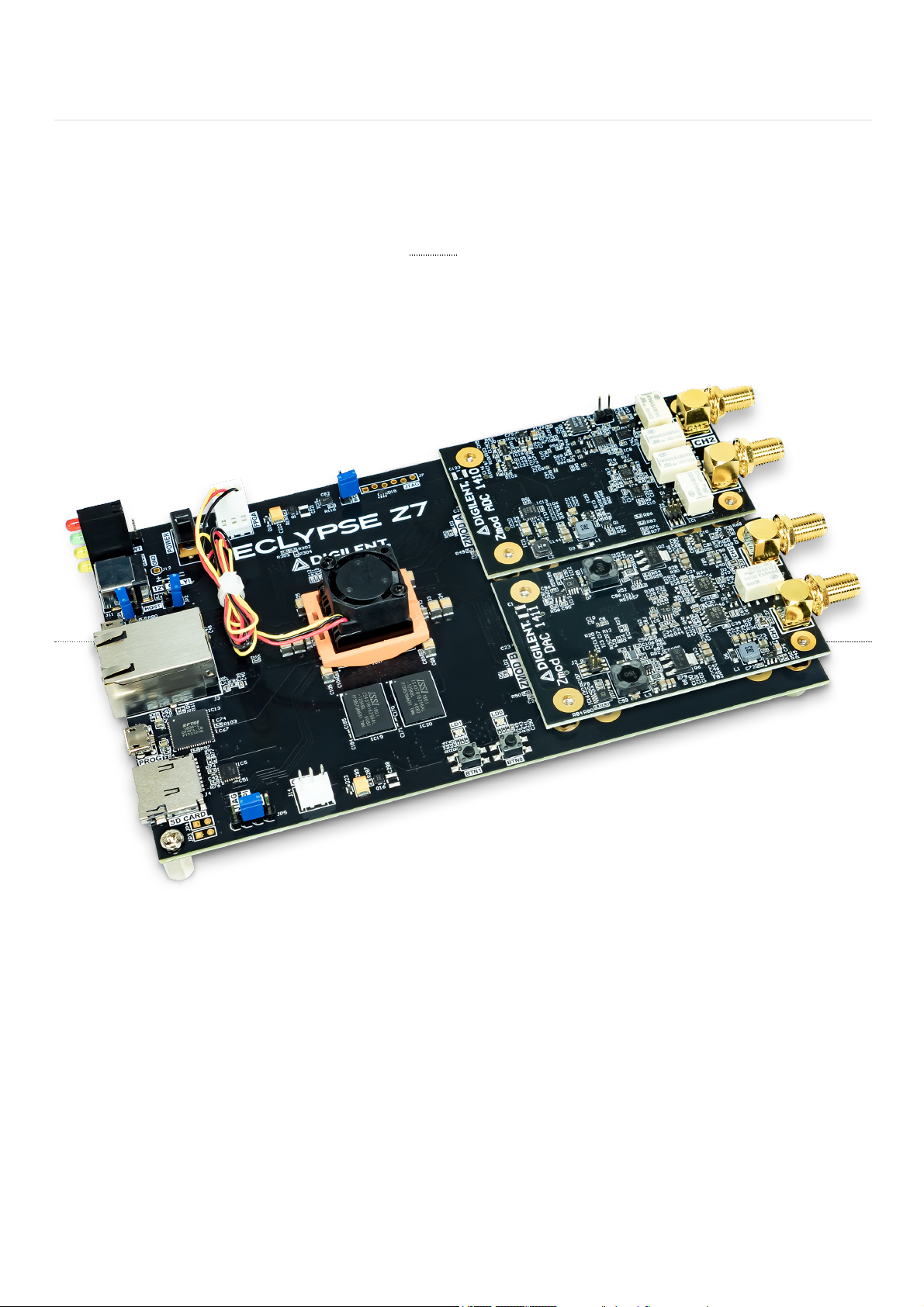
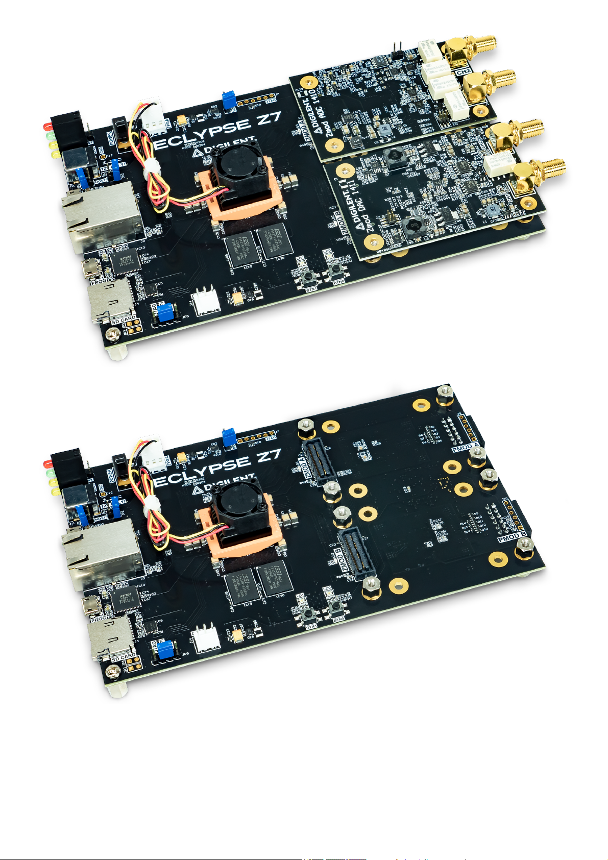
The Eclypse Z7 is a powerful prototyping platform, featuring Xilinx's Zynq-7000 APSoC. Two SYZYGY interface
connectors are featured, enabling high speed modular systems.
Eclypse is designed to enable high speed analog data capture and analysis right out of the box. It is a platform for research
and rapid prototyping of test and measurement applications, potentially including software defined radio, ultrasound, other
medical devices, and much more. As a host board forZmods, applications for the Eclypse can vary significantly between
system configurations.
Petalinux is supported out of the box. Pre-built Linux images are accompanied by a software API for bulk data transfer.
This system allows new users to get started without touching hardware until desired. The software supports a variety of
common programming languages, including Python, C/C++, and more. Digilent offers fully open and customizable
hardware designs, Linux images, and Linux software applications.
Eclypse Z7 Hardware Reference Manual
Page 2
Page 3
Zynq-7000 APSoC (XC7Z020-1CLG484C)
667 MHz dual-core Cortex-A9 processor
DDR3L memory controller with 8 DMA channels and 4 High Performance AXI3 Slave ports
High-bandwidth peripheral controllers: 1G Ethernet, USB 2.0, SDIO
Low-bandwidth peripheral controllers: SPI, UART, CAN, I2C
Programmable from JTAG, Quad-SPI flash, and microSD card
Programmable logic equivalent to Artix-7 FPGA
Memory
1 GiB DDR3L with 32-bit bus @ 1066 MT/s
16MBQuad-SPI Flash with factory programmed 128-bit random number and 48-bit globally unique EUI48/64™ compatible identifier
Features
Page 4
microSD card slot
Power
Powered from external 12V 5A supply
Platform MCU for configuration of adjustable power supplies and temperature management
USB and Ethernet
Gigabit Ethernet PHY
USB-JTAG programming circuitry
USB-UART bridge
USB micro AB port with USB 2.0 PHY with Host/Device/OTG capabilities
Zmod Ports
2 ports following the SYZYGY Standard interface specification
Compatible with a variety of SYZYGY pods, allowing for a wide variety of applications
Dedicated differential clocks for input and output
8 differential I/Os per port
16 single-ended I/Os per port
DNA interfaces connected to Platform MCU allowing for various auto-negotiated power supply
configurations
Pmod Ports
2 twelve-pin ports for a total of 16 FPGA-connected I/Os
High speed voltage translation and protection circuitry
UserGPIO
2 push-buttons
2 RGB LEDs
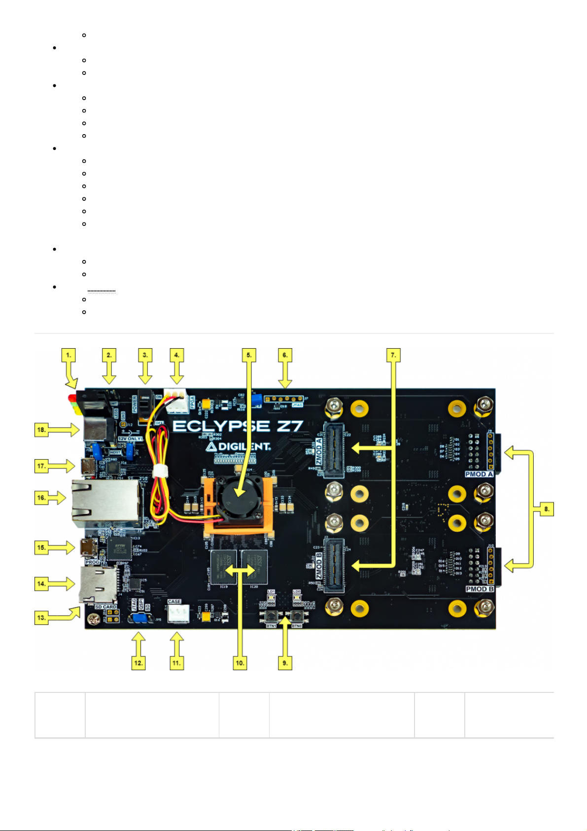
Eclypse Z7 Callout Diagram
Callout
# Description
Callout
# Description
Callout
# Description
Page 5

The Eclypse Z7 includes an FPGA fan to dissipate extra heat generated from running complex fast-switching designs. A
USB A to Micro B programming cable, a USB A to Micro A cable, and a 12V 5A power supply, are included with the
Eclypse Z7.
An Eclypse Z7 Enclosure Kit may optionally be added on, which provides a sturdy case for the Eclypse platform. The
Enclosure Kit includes a case fan for additional cooling, and exposes the connectors of loaded Zmod ADCs and DACs, as
well as the Eclypse Z7's Pmod expansion connectors, power switch, status LEDs, and more.
For more information on purchasing an Eclypse Z7, see theEclypse Z7 Product Page.
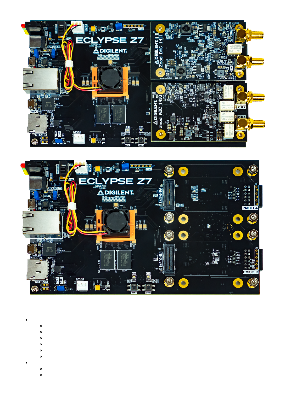
Digilent Zmodsmay also be purchased individually or bundled with the Eclypse Z7. Expansion connectors such as these,
or other SYZYGY modules, are required to fully leverage the high-speed I/O capabilities of the Eclypse platform.
Zynq platforms are well-suited to be embedded Linux targets, and the Eclypse Z7 is no exception. Digilent provides
software examples targeting custom Petalinux projects, including support for each Digilent Zmod for high-speed I/O
capabilities.
The Eclypse Z7 is fully compatible with Xilinx’s high-performance Vivado ® Design Suite. This tool set melds FPGA logic
design and embedded ARM software development into an easy to use, intuitive design flow. It can be used for designing
systems of any complexity, from a complete operating system running multiple server applications, down to a simple baremetal program that controls some LEDs. It is also possible to treat the Zynq AP SoC as a standalone FPGA for those not
interested in using the processor in their design. The Eclypse Z7 is supported under Vivado's free WebPACK™ license,
which means the software is completely free to use, including the Logic Analyzer and High-level Synthesis (HLS) features.
The Logic Analyzer assists with debugging logic that is running in hardware, and the HLS tool allows C code to be directly
compiled into HDL.
Digilent currently does not provide hardware platforms or examples for Xilinx's Vitis Unified Software Platform, however
Vitis support is planned for the near future.
Design resources, example projects, and tutorials are available for download at theEclypse Z7 Resource Center.
Callout
# Description
Callout
# Description
Callout
# Description
1 Board Indicator LEDs
(LD4)
7 SYZYGY Ports 13 Reset Buttons (und
board)
2 Header for Case Power
Switch
8 Pmod Ports 14 microSD Card Slo
3 Power Switch 9 User Buttons and LEDs 15 USB JTAG/UART
4 FPGA Fan Header 10 DDR3L Memory 16 Ethernet Port
5 Zynq-7000 SoC and
FPGA Fan
11 Case Fan Header 17 USB AB
Host/Device/OT
6 External JTAG Port 12 Programming Mode Select
Jumper
18 Power Supply Con
Purchasing Options
Software Support
Zynq APSoC Architecture
Page 6
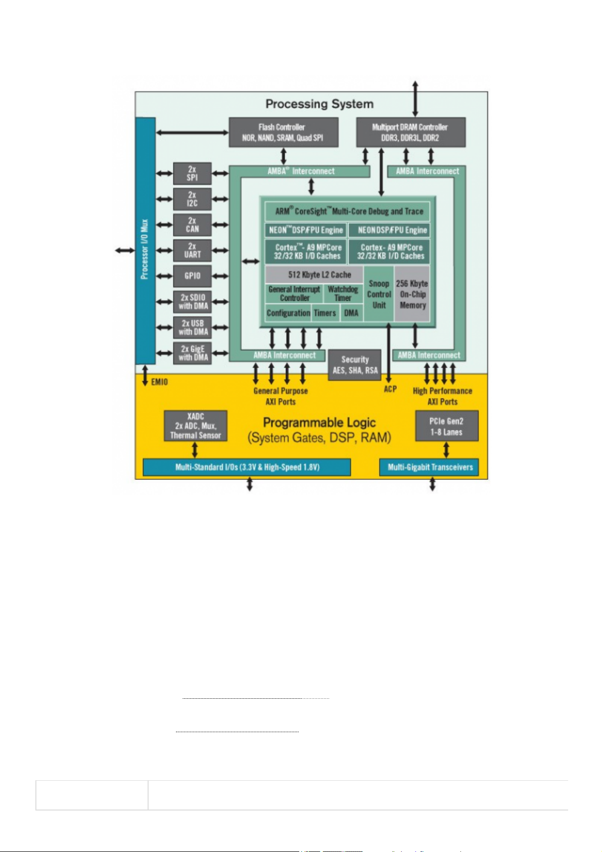
The Zynq APSoC is divided into two distinct subsystems: The Processing System (PS) and the Programmable Logic (PL).
The figure below shows an overview of the Zynq APSoC architecture, with the PS colored light green and the PL in yellow.
Note that the PCIe Gen2 controller and Multi-gigabit transceivers are not available on the Zynq-7020 device.
The PL is nearly identical to a Xilinx 7-series Artix FPGA, except that it contains several dedicated ports and buses that
tightly couple it to the PS. The PL also does not contain the same configuration hardware as a typical 7-series FPGA, and it
must be configured either directly by the processor or via the JTAG port.
The PS consists of many components, including the Application Processing Unit (APU, which includes 2 Cortex-A9
processors), Advanced Microcontroller Bus Architecture (AMBA) Interconnect, DDR3 Memory controller, and various
peripheral controllers with their inputs and outputs multiplexed to 54 dedicated pins (called Multiplexed I/O, or MIO pins).
Peripheral controllers that do not have their inputs and outputs connected to MIO pins can instead route their I/O
through the PL, via the Extended-MIO (EMIO) interface. The peripheral controllers are connected to the processors as
slaves via the AMBA interconnect, and contain readable/writable control registers that are addressable in the processors’
memory space. The programmable logic is also connected to the interconnect as a slave, and designs can implement
multiple cores in the FPGA fabric that each also contain addressable control registers. Furthermore, cores implemented in
the PL can trigger interrupts to the processors and perform DMA accesses to DDR3 memory.
There are many aspects of the Zynq APSoC architecture that are beyond the scope of this document. For a complete and
thorough description, refer to theZynq Technical Reference manual.
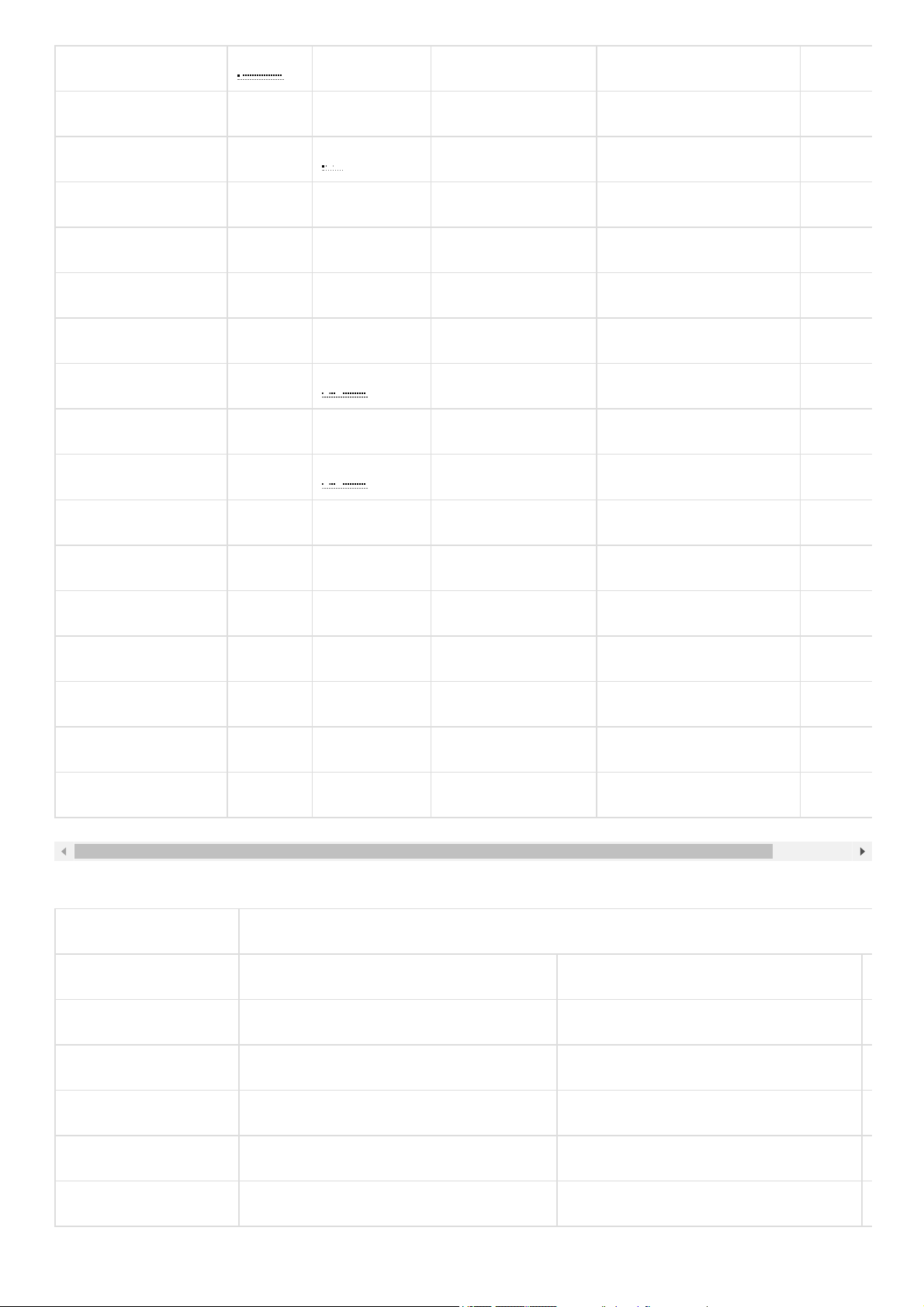
The tables in the dropdowns below depict the external components connected to the MIO pins of the Eclypse Z7. The
Vivado board files found on theEclypse Z7 Resource Centercan be used to properly configure the PS to work with these
peripherals. It is also possible to use the example projects found on the resource center as a starting point for custom
designs.
MIO 0-15 : Bank 500
MIO 500 3.3 V Peripherals
Page 7
MIO 16-53 : Bank 501
Pin GPIO SPI Flash ENET 0 SYZYGY UART 0
0 (N/C)
1 CS
2 DQ0
3 DQ1
4 DQ2
5 DQ3
6 SCLK
7 (N/A)
8 SCLKFB
9 Ethernet Reset
10 (N/A)
11 (N/A)
12 DNA SCL (I2C 0)
13 DNA SDA (I2C 0)
14 UART In
15 UART O
MIO 501 1.8V Peripherals
Pin ENET 0 USB 0
16 TXCK
17 TXD0
18 TXD1
19 TXD2
20 TXD3
Page 8

21 TXCTL
22 RXCK
23 RXD0
24 RXD1
25 RXD2
26 RXD3
27 RXCTL
28 DATA4
29 DIR
30 STP
31 NXT
32 DATA0
33 DATA1
34 DATA2
35 DATA3
36 CLK
37 DATA5
38 DATA6
39 DATA7
40
41
42
43
44
45
46 USB Reset
Page 9
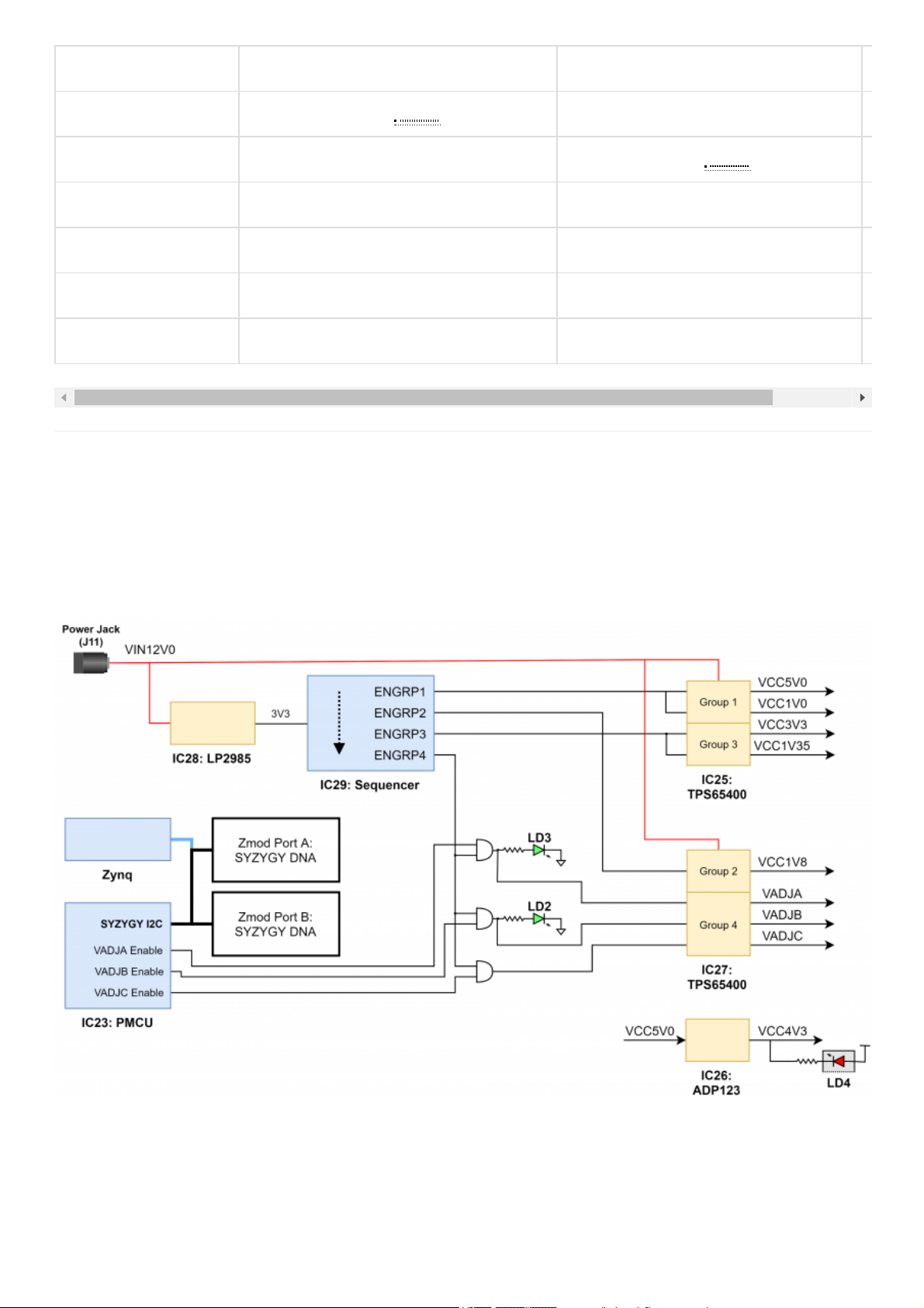
The Eclypse Z7 power circuitry was carefully designed to meet the requirements of the Zynq-7000 and all peripherals while
providing the flexibility needed to power a variety of different configurations of Zmod/SYZYGY modules.
An overview of the power circuit is shown in Figure 1.1.
Figure 1.1: Power circuit overview
All on-board power supplies are enabled or disabled by the power switch (SW1) or by an external SPST switch connected
to the SWT header (J13).
Note:If an external switch is used, SW1 should be placed in the “OFF” position, as the two will be placed in parallel.
The power indicator LED, the topmost LED of the circuit board indicator (LD4), is illuminated red when all supply rails
reach their nominal voltage.
47
48 Ethernet Interrupt (GPIO)
49 USB Overcurrent (GPIO)
50 (N/C)
51 (N/C)
52 MDC
53 MDIO
Functional Description
1. Power Supplies
Page 10

Two additional indicator LEDs are illuminated when the VIO supplies associated with the two Zmod Ports are powered.
LD2 is associated with Zmod Port A and the VADJA rail. LD3 is associated with Zmod Port B and the VADJB rail.
The Eclypse Z7 should be powered via a wall wart supply with barrel jack, via the barrel connector (J11). The supply must
use a center-positive 2.1 mm internal-diameter plug and deliver between 11.5V and 12.5V DC. It should also be able to
provide at least 5 A (60 Watts) in order to support power hungry Zynq projects and external peripherals. A compatible
power supply ships with the Eclypse Z7.
Table 1.1.1: Eclypse Z7 Power Input Specifications
Table 1.2.1 describes the characteristics of the Eclypse Z7's on-board power rails. It can be used to estimate power
consumption for a project, or determine how much current attached peripherals can draw before being limited.
Table 1.2.1: Eclypse Z7 Power Rail Specifications
Connector
Type
Connector
Label
Schematic Net
Name
Min/Rec/Max Voltage
(V)
Max Current
Consumption
Barrel jack J11 VIN12V0 11.5/12/12.5 5 A / 60 W
Net
Name
Upstream
Net Name
Power
IC Type
Power
IC Label
Min/Typ/Max
Voltage
Max.
Current Major Devices and Conn
VCC5V0 VIN12V0 Buck IC27 5.0V +-5% 3A Zmods, USB OTG VBUS,
LEDs, Case Fan
VCC1V0 VIN12V0 Buck IC27 1.0V +-5% 1A Zynq, Ethernet, USB OTG
JTAG/UART, microSD
DDR1V35 VIN12V0 Buck IC25 1.35V +-5% 2A Zynq, DDR3L
DDRVTT VIN12V0 LDO IC21 0.675V +-5% 0.45A DDR3L
VCC3V3 VIN12V0 Buck IC25 3.3V +-5% 3.3A Zynq, Zmods, Pmods, USB
USB JTAG/UART, microS
VCC4V3 VCC5V0 LDO IC26 4.3V +-5% 0.3A Pmods
VADJA VIN12V0 Buck IC27 1.2V to 3.3V;
+-5%
1.8A FPGA, Zmod Port A
VADJB VIN12V0 Buck IC27 1.2V to 3.3V;
+-5%
1.8A FPGA, Zmod Port B
VADJC VIN12V0 Buck IC25 2.5 to 5.5V; +-
5%
0.3A FPGA Fan
1.1. Power Input Source
1.2. Power Specifications
Page 11

The power budget of VCC5V0 is shared by the SYZYGY ports, USB OTG VBUS, RGB LEDs, and Case Fan. As such, the
actual maximum current achievable by each peripheral varies with the Eclypse Z7's system configuration. Under worst-case
conditions, VCC5V0 is capable of outputting a minimum of 3A of continuous current. In this scenario, 1A is budgeted for
each Zmod
The Platform MCU (PMCU) enumerates the SYZYGY ports and determines the power needs of each Zmod installed in
the system. The 5V power budget of the Eclypse is then determined based on the needs of each Zmod, as well as the USB
OTG VBUS, RGB LEDs, and Fan. Table 1.2.2 describes the 5V power budget of the Eclypse Z7 in more detail.
Table 1.2.2: Eclypse 5V Power Budget
The two SYZYGY ports share a budget of 2A from the 3.3V supply. The two Pmod ports share a budget of 0.5A, which is
allocated to the SYZYGY ports if no Pmods are installed.
Due to the requirements of the custom power sequencer (IC29), Digilent recommends that peripheral modules (Pmods and
Zmods) attached to and powered by the Eclypse meet the specifications described in Table 1.2.3.
Table 1.2.3: Recommended Maximum Additional Capacitance for Add-on Modules
Device or Connector Max Current (mA)
RGB LEDs 124.8
USB OTG VBUS 500
Zmod Port A 1000
Zmod Port B 1000
Case Fan 250
Port Rail Max Capacitance (µF)
Zmod Port A VCC5V0 500
Zmod Port A VCC3V3 500
Zmod Port A VIO 1000
Zmod Port B VCC5V0 500
Zmod Port B VCC3V3 500
Zmod Port B VIO 1000
Pmod Port A VCC3V3 500
Pmod Port B VCC3V3 500
1.3. Power Sequencing
Page 12

A custom power sequencer (IC29) is used to sequence the power supplies on in the correct order when the power switch is
placed in the “ON” position. The power supplies shut down in the opposite order when the power switch is moved to the
“OFF” position. The startup sequence is as follows:
1. VCC5V0, FAN5V0
2. VCC1V0
3. VCC1V8
4. DDR1V35, DDRVTT
5. VCC3V3
6. VCC4V3
7. VADJA, VADJB, VADJC
The sequencer is provided 3.3V power by a dedicated regulator, a Texas Instruments LP2985 (IC28).
The sequencer ensures that the supply rails follow the Xilinx-recommended start-up and shut-down sequences.
Note:VADJA, VADJB, and VADJC are controlled by the Platform MCU (PMCU) and may or may not be enabled, depending on the
PMCU configuration and presence (or lack thereof) of any pods connected to Zmod A or Zmod B. If the sum of the currents required by each
Zmod is in excess of the 3A budget for VCC5V0, VADJA and VADJB are not turned on.
The FPGA fan is to be connected to the Eclypse Z7 via fan header J8 (labeled “FPGA”) and is powered by VADJC, an
adjustable rail controlled by the Platform MCU. The FPGA fan's speed can be configured to Automatic (the default factory
setting), High, Medium, Low, or Off, by communicating with the PMCU through its I2C interface. This configuration is
preserved by the PMCU in anEEPROMwhen the Eclypse's power is cycled. Additional information and configuration
settings, including RPM and speed controls, can be accessed through the PMCU's I2C interface.
In addition to the FPGA fan, the Eclypse Z7 can power a Case Fan, connected to the board via fan header J14 (labeled
“CASE”). This fan is powered by the 5V rail, and is limited to 250 mA. A compatible fan is included in theEclypse Z7
Enclosure Kit.
As noted in previous sections, the Eclypse Z7 uses an Atmega328PB microcontroller (IC10), referred to as the Platform
MCU (PMCU), to implement the SmartVIO requirements of the SYZYGY standard, as well as to monitor the Zynq die
temperature, and to control the Eclypse's fan.
When the Eclypse is turned on, the PMCU enumerates the pods attached to the Eclypse's SYZYGY ports and retrieves
their DNA, in order to correctly configure the variable supplies.
After SYZYGY enumeration is complete, the PMCU configures itself as an I2C slave device with a chip address of 0x60.
Control of the I2C bus is then handed over to the Zynq's I2C 1 peripheral (MIO[12:13]). The Digilent Eclypse Utility
(decutil) is included in Petalinux images for the Eclypse Z7 and can be used to get status information from and change
some settings of the PMCU. For more information on the PMCU's register space and communication protocol, see the
PMCU specification (PDF Download). For more information on decutil, see theDigilent Eclypse Utility Documentation.
The following tables describe the features of the Platform MCU supported by the Eclypse Z7:
Table 1.6.1: Platform MCU Connectivity Map
PMCU Interface Connection
TEMPERATURE A Zynq Die Temperature
PORT_A, VADJ_A Zmod A
PORT_B, VADJ_B Zmod B
FAN_1 FPGA Fan
FAN_2 Case Fan
1.4. FPGA Fan
1.5. Case Fan
1.6. Platform MCU
Page 13
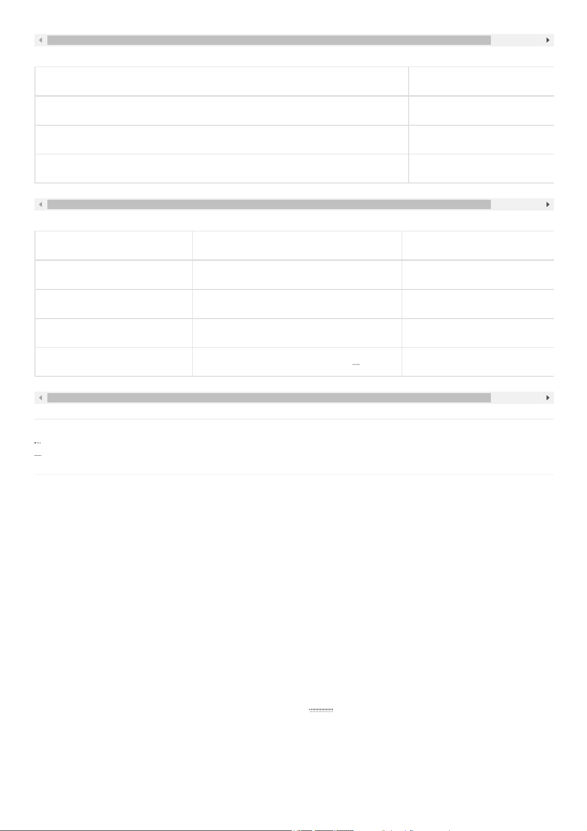
Table 1.6.2: Supported Platform MCU Optional Features
Table 1.6.3: Supported Platform MCU Fan COntrol Features
The optional FPGA fan included with the Eclypse Z7 supports RPM measurement
The case fan included in the Eclypse Z7 Enclosure Kit does not support RPM measurement
Unlike Xilinx FPGA devices, AP SoC devices such as the Zynq-7020 are designed around the processor, which acts as a
master to the programmable logic fabric and all other on-chip peripherals in the processing system. This causes the Zynq
boot process to be more similar to that of a microcontroller than an FPGA. This process involves the processor loading
and executing a Zynq Boot Image, which includes a First Stage Bootloader (FSBL), a bitstream for configuring the
programmable logic (optional), and a user application.
The boot process is broken into three stages:
After the Eclypse Z7 is powered on or the Zynq is reset (in software or by pressing the PS-SRST button, BTNR), one of
the processors (CPU0) begins executing an internal piece of read-only code called the BootROM. If and only if the Zynq
was just powered on, the BootROM will first latch the state of the mode pins into the mode register (the mode pins are
attached to JP5 on the Eclypse Z7). If the BootROM is being executed due to a reset event, then the mode pins are not
latched, and the previous state of the mode register is used. This means that the Eclypse Z7 needs a power cycle to register
any change in the programming mode jumper (JP5). Next, the BootROM copies an FSBL from the form of non-volatile
memory specified by the mode register to the 256 KB of internalRAMwithin the APU (called On-Chip Memory, or
OCM). The FSBL must be wrapped up in a Zynq Boot Image in order for the BootROM to properly copy it. The last thing
the BootROM does is hand off execution to the FSBL in OCM.
During this stage, the FSBL first finishes configuring the PS components, such as the DDR memory controller. Then, if a
bitstream is present in the Zynq Boot Image, it is read and used to configure the PL. Finally, the user application is loaded
into memory from the Zynq Boot Image, and execution is handed off to it.
Optional Features Supported
DDRVCCSEL Control No
INIT_B Control No
USB Hub Support No
Feature FAN_1 (FPGA Fan) FAN_2 (Case Fan)
Enable / Disable Yes No
Fixed Speed Control Yes No
Automatic Speed Control Yes No
RPM Measurement Yes (if supported by installed fan) Yes (if supported by installed fan
1)
1)
2)
2. Zynq Configuration
Stage 0
Stage 1
Page 14
The last stage is the execution of the user application that was loaded by the FSBL. This can be any sort of program, from a
simple bare-metal “Hello World” application, to a Second Stage Boot loader used to boot an operating system like Linux.
For a more thorough explanation of the boot process, refer to Chapter 6 of theZynq Technical Reference Manual.
The Zynq Boot Image is created using Vivado and Xilinx Software Development Kit (Xilinx SDK). For information on
creating this image please refer to the available Xilinx documentation for these tools.
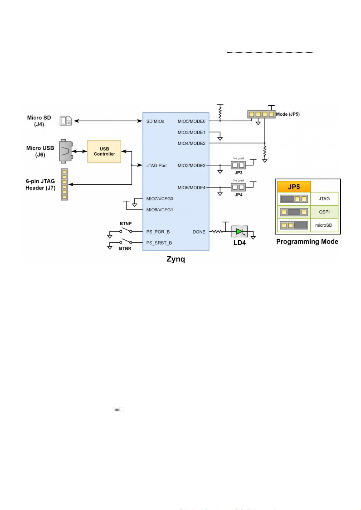
The Eclypse Z7 supports three different boot modes: microSD, Quad SPI Flash, and JTAG. The boot mode is selected
using the Mode jumper (JP5), which affects the state of the Zynq configuration pins after power-on. Figure 2.1 depicts how
the Zynq configuration pins are connected on the Eclypse Z7.
Figure 2.1: Eclypse Z7 configuration pins.
The three boot modes are described in the following sections.
The Eclypse Z7 supports booting from a microSD card inserted into connector J4 (labeled “SD CARD”). The following
procedure will allow you to boot the Zynq from microSD with a standard Zynq Boot Image created with the Xilinx tools:
1. Format the microSD card with a FAT32 file system.
2. Copy the Zynq Boot Image created with Xilinx SDK to the microSD card.
3. Rename the Zynq Boot Image on the microSD card to BOOT.bin.
4. Eject the microSD card from your computer and insert it into J4 on the Eclypse Z7.
5. Attach a power supply to the Eclypse Z7 via the barrel jack (J11).
6. Place a single jumper on JP5, shorting the two rightmost pins (labeled “SD”).
7. Turn the board on by flipping the power switch to the ON position. The board will now boot the image on the
microSD card.
The Eclypse Z7 has an onboard 16MBQuad-SPI Flash that the Zynq can boot from. Documentation available from
Xilinx describes how to use Xilinx SDK to program a Zynq Boot Image into a Flash device attached to the Zynq. Once the
Quad SPI Flash has been loaded with a Zynq Boot Image, the following steps can be followed to boot from it:
1. Attach a power supply to the Eclypse Z7 via the barrel jack (J11).
2. Place a single jumper on JP5, shorting the two center pins (labeled “QSPI”).
3. Turn the board on by flipping the power switch to the ON position. The board will now boot the image stored in
the Quad SPI flash.
Stage 2
2.1. microSD Boot Mode
2.2. Quad SPI Boot Mode
2.3. JTAG Boot Mode
Page 15

When placed in JTAG boot mode, with the two leftmost pins of JP5 shorted (labeled “JTAG”), the processor will wait until
software is loaded by a host computer using the Xilinx tools. After software has been loaded, it is possible to either let the
software begin executing, or step through it line by line using Xilinx SDK.
It is also possible to directly configure the PL over JTAG, independent of the processor. This can be done using the Vivado
Hardware Server.
The Eclypse Z7 is configured to boot in Cascaded JTAG mode, which allows the PS to be accessed via the same JTAG
port as the PL. It is also possible to boot the Eclypse Z7 in Independent JTAG mode by shorting unloaded jumper JP3.
This will cause the PS to not be accessible from the onboard JTAG circuitry, and only the PL will be visible in the scan
chain. To access the PS over JTAG while in independent JTAG mode, users will have to route the signals for the PJTAG
peripheral over EMIO, and use an external device to communicate with it.
The Eclypse Z7 includes two Micron MT41K256M16TW-107 DDR3L memory components creating a single rank, 32-bit
wide interface and a total of 1 GiB (Gibi-byte, or 1,073,741,824 bytes) of capacity. The DDR3L is connected to the hard
memory controller in the Processor Subsystem (PS), as outlined in the Zynq documentation.
Note:The Eclypse Z7 may alternatively use an ISSI IS43TR16256A(L)-125KBL DDR3L memory. This part is compatible with the
same timings as the Micron part.
The PS incorporates an AXI memory port interface, a DDR controller, the associated PHY, and a dedicated I/O bank.
DDR3L memory interface speeds up to 533 MHz/1066 MT/s are supported.
The Eclypse Z7 was routed with 40 ohm (+/-10%) trace impedance for single-ended signals, and differential clock and
strobes set to 80 ohms (+/-10%). A feature called DCI (Digitally Controlled Impedance) is used to match the drive
strength and termination impedance of the PS pins to the trace impedance. On the memory side, each chip calibrates its
on-die termination and drive strength using a 240 ohm resistor on the ZQ pin.
Both the memory chips and the PS DDR bank are powered from the 1.35V supply. The mid-point reference of 0.675V is
created with a simple resistor divider and is available to the Zynq as external reference.
For proper operation it is essential that the PS memory controller is configured properly. Settings range from the actual
memory flavor to the board trace delays. For your convenience, the Eclypse Z7 Vivado board files are available on
theEclypse Z7 Resource Centerand automatically configure the Zynq Processing System IP core with the correct
parameters.
For best DDR3L performance, DRAM training is enabled for write leveling, read gate, and read data eye options in the PS
Configuration Tool in Xilinx tools. Training is done dynamically by the controller to account for board delays, process
variations and thermal drift. Optimum starting values for the training process are the board delays (propagation delays) for
certain memory signals.
Board delays are specified for each of the byte groups. These parameters are board-specific and were calculated from the
PCB trace length reports. The DQS to CLK Delay and Board Delay values are calculated specific to the Eclypse Z7
memory interface PCB design.
For more details on memory controller operation, refer to the XilinxZynq Technical Reference manual.
The Eclypse Z7 features a Spansion S25FL128S 4-bit Quad-SPI serial NOR flash. The key device attributes are:
Part number S25FL128S
16MBof memory
1-bit, 2-bit, and 4-bit bus widths supported
General use clock speeds up to 100 MHz, translating to 400 Mbps in Quad-SPI mode
Zynq configuration clock speeds up to 94 MHz
Powered from 3.3V
The Flash memory is used to provide non-volatile code and data storage. It can be used to initialize the PS and PL of the
Zynq device with a Zynq Boot Image (also known as BOOT.BIN) generated using Xilinx tools such as Petalinux or Xilinx
SDK. For information on booting the Eclypse Z7 with a Zynq Boot image, see section “2.2 Quad SPI Boot Mode”.
3. DDR3L Memory
4. Quad-SPI Flash
Page 16

The Flash is also commonly used to store non-configuration data needed by the application. If doing this from a bare-metal
application, The flash memory can be freely accessed using standalone libraries included with a Xilinx SDK BSP project. If
doing this from a Petalinux generated embedded Linux system, the Flash can be partitioned as desired and
mounted/accessed like a standard MTD block device. See the Petalinux and Xilinx SDK documentation for more
information.
The Flash connects to the Quad-SPI Flash controller of the Zynq-7000 PS via pins in MIO Bank 0/500 (specifically
MIO[1:6,8]), as outlined in the Zynq Technical Reference Manual. Quad-SPI feedback mode is used, thus
qspi_sclk_fb_out/MIO[8] is left to freely toggle and is connected only to a 20K pull-up resistor to 3.3V. This allows a
Quad-SPI clock frequency greater than FQSPICLK2. The details of these connections do not need to be known when
using the Eclypse Z7 Vivado Board files, as they will automatically configure your project to work correctly with the onboard Flash.
A globally unique MAC address is programmed into the One-Time-Programmable (OTP) region of the Flash on each
Eclypse Z7 at the factory. For more information on this, see section11. Ethernet. The MAC address can also be found on
a sticker attached to the board.
The OTP region also includes a factory-programmed read-only 128-bit random number. The very lowest address range
[0x00;0x0F] can be read to access the random number. See the Spansion S25FL128S datasheet for information on this
random number and accessing the OTP region.
The Eclypse Z7 provides a 33.3333 MHz clock to the Zynq PS_CLK input, which is used to generate the clocks for each
of the PS subsystems. The 33.3333MHzinput allows the processor to operate at a maximum frequency of 667 MHz and
the DDR3 memory controller to operate at a maximum clock rate of 533MHz(1066 MT/s). The Eclypse Z7 board files,
available on theEclypse Z7 Resource Center, will automatically configure the Zynq processing system IP core in Vivado to
work with all PS attached devices, including the 33.3333MHzinput oscillator.
The PS has a dedicated PLL capable of generating up to four reference clocks, each with settable frequencies, that can be
used to clock custom logic implemented in the PL. Additionally, The Eclypse Z7 provides an external 125MHzreference
clock directly to pin D18 of the PL. The external reference clock allows the PL to be used completely independently of the
PS, which can be useful for simple applications that do not require the processor.
The PL of the Zynq-Z7020 also includes four MMCM’s and four PLL’s that can be used to generate clocks with precise
frequencies and phase relationships. Any of the four PS reference clocks or the 125MHzexternal reference clock can be
used as an input to the MMCMs and PLLs. For a full description of the capabilities of the Zynq PL clocking resources,
refer to the7 Series FPGAs Clocking Resources User Guideavailable from Xilinx.
Xilinx offers the Clocking Wizard IP core to assist in integrating the MMCM's and PLL's into a design. This wizard will
properly instantiate the needed MMCMs and PLLs based on the desired frequencies and phase relationships specified by
the user. The wizard will then output an easy-to-use wrapper component around these clocking resources that can be
inserted into the user’s design. The clocking wizard can be accessed from within the Vivado and IP Integrator tools.
Figure 5.1 outlines the clocking scheme used on the Eclypse Z7. Note that the reference clock output from the Ethernet
PHY is used as the 125MHzreference clock to the PL, in order to cut the cost of including a dedicated oscillator for this
purpose. Keep in mind that CLK125 will be disabled when the Ethernet PHY is held in hardware reset by driving the
PHYRSTB signal low.
5. Oscillators/Clocks
Page 17
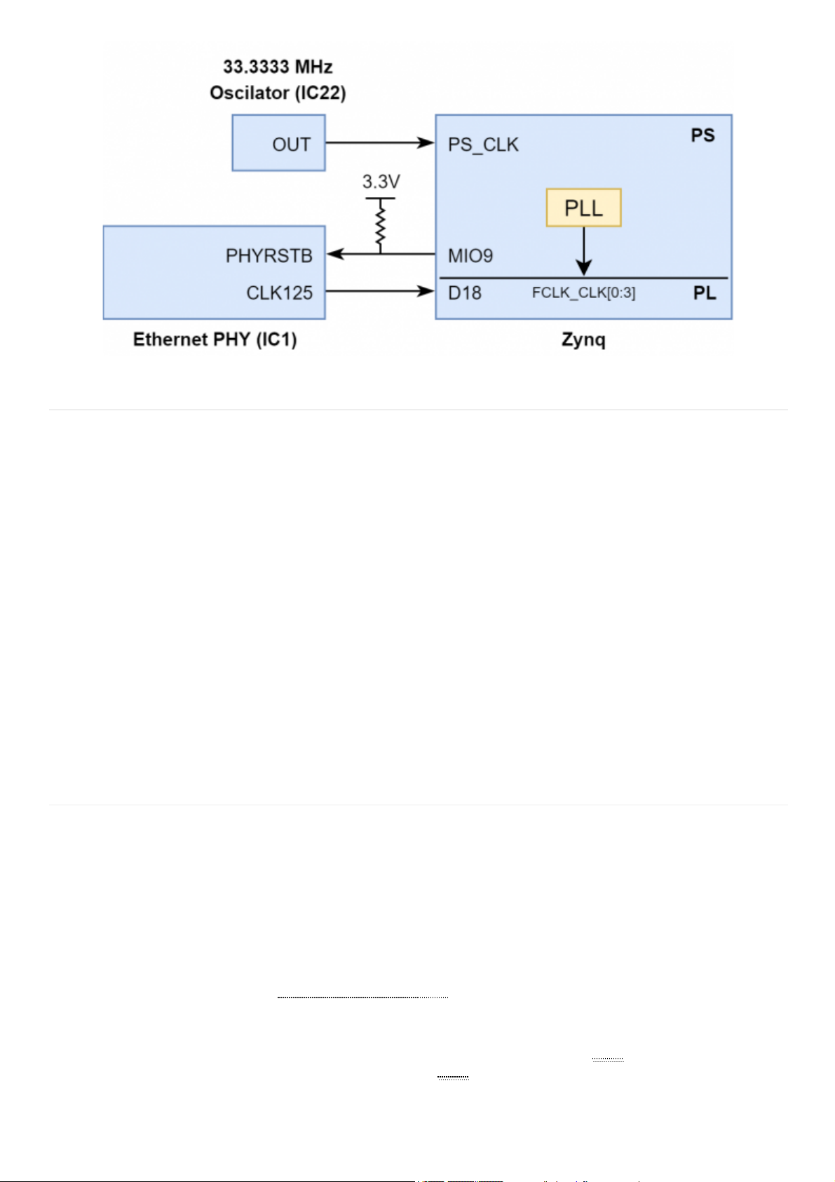
Figure 5.1: Eclypse Z7 clocking.
The Eclypse Z7 provides several different methods of resetting the Zynq-7000 device, as described in the following
sections:
The Zynq PS supports external power-on reset signals. The power-on reset is the master reset of the entire chip. This signal
resets every register in the device capable of being reset. The Eclypse Z7 drives this signal from the VCC4V3 supply, the
final non-adjustable supply to be brought up in the power-on sequence, in order to hold the system in reset until all power
supplies are valid. A push-button, labeled BTNP, can be used to toggle the power-on reset signal. BTNP is located on the
underside of the Eclypse Z7, below the SD card slot.
The external system reset button, labeled BTNR, resets the Zynq device without disturbing the debug environment. For
example, the previous break points set by the user remain valid after system reset. Due to security concerns, system reset
erases all memory content within the PS, including the On-Chip-Memory (OCM). The PL is also cleared during a system
reset. System reset does not cause the boot mode strapping pins to be re-sampled. After changing the boot mode jumper a
power cycle is needed to act on the new setting. BTNR is located on the underside of the Eclypse Z7, below the SD card
slot.
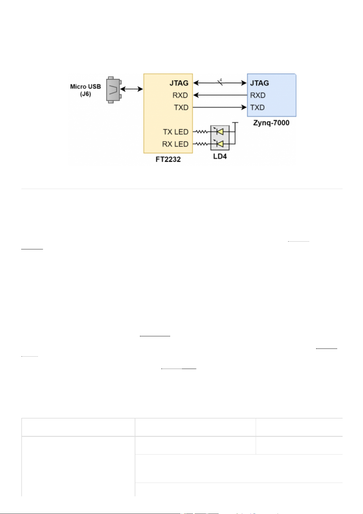
The Eclypse Z7 includes an FTDI FT2232HQ USB-UART bridge (attached to connector J6) that lets PC applications
communicate with the board using standard COM port commands (or the tty interface in Linux). Drivers are automatically
installed in Windows and newer versions of Linux when the Eclypse Z7 is attached. Serial port data is exchanged with the
Zynq using a two-wire serial port (TXD/RXD). After the drivers are installed, I/O commands can be used from the PC
directed to the COM port to produce serial data traffic on the Zynq pins. The port is tied to PS (MIO) pins and can be
used in combination with the UART 0 controller.
The Zynq presets file (available in theEclypse Z7 Resource Center) takes care of mapping the correct MIO pins to the
UART 0 controller and uses the following default protocol parameters: 115200 baud rate, 1 stop bit, no parity, 8-bit
character length.
Two status LEDs provide visual feedback on traffic flowing through the port: the transmitLED(the lower of the two
yellow LEDs in the circuit board indicator, LD4) and the receiveLED(the upper of the two yellow LEDs in the circuit
board indicator, LD4). Signal names that imply direction are from the point-of-view of the DTE (Data Terminal
Equipment), in this case the PC.
6. Reset Sources
6.1. Power-on Reset
6.2. Processor Subsystem Reset
7. USB-UART Bridge (Serial Port)
Page 18
The FT2232HQ is also used as the controller for the Digilent USB-JTAG circuitry, but the USB-UART and USB-JTAG
functions behave entirely independent of one another. Programmers interested in using the UART functionality of the
FT2232 within their design do not need to worry about the JTAG circuitry interfering with the UART data transfers, and
vice-versa. The combination of these two features into a single device allows the Zybo Z7 to be programmed and
communicated with via UART from a computer attached with a single Micro USB cable.
The connections between the FT2232HQ and the Zynq-7000 are shown in Figure 7.1.
Figure 7.1: UART Connections
The Eclypse Z7 features two Zmod ports, which use SYZYGY Standard interfaces to communicate with installed
SYZYGY pods. Both ports are compatible with version 1.1 of the SYZYGY specification from Opal Kelly.
SYZYGY SmartVIO functionality is implemented by the Eclypse's Platform MCU, as discussed in the1 Power
Suppliessection of this document. Each port's SYZYGY DNA is connected to both the Platform MCU and the Zynq's
I2C 0 peripheral (MIO12:13) through a single I2C bus. Once the board is fully powered on, and the PMCU has configured
itself in I2C slave mode, SYZYGY DNA data can be read directly from the pods, and the negotiated voltages and currents
can be read from the PMCU over this bus.
Warning:SYZYGY pods are NOT hot-swappable. Connecting or disconnecting a pod from the Eclypse while the board is powered on may
cause damage to the pod and/or the board, and is to be avoided.
Each SYZYGY Standard interface contains 16 single-ended I/O pins, 8 differential I/O pairs (which can alternatively be
used as 16 additional single-ended I/O pins), and two dedicated differential clocks - one for input and one for output. Each
Zmod port has a I/O bank of the Zynq dedicated to it, which is powered by a dedicated adjustable rail, configured by the
Platform MCU as the Eclypse is powered on. Template constraints for each Zmod port can be found in the Eclypse Z7's
Master XDC file, available through Digilent'sdigilent-xdcrepository on Github.
Digilent provides Eclypse-compatible low-level IPs, scripted Vivado flows, and software libraries to support eachDigilent
Zmod.
For more information on the SYZYGY standard, seesyzygyfpga.io.
The Eclypse's Zmod ports are compatible with a variety of different SYZYGY pods. Information required to determine if
the Eclypse is compatible with a certain pod is summarized in Table 8.1.1.
Table 8.1.1: SYZYGY Compatibility Table
Parameter Port A (STD) Port B (STD)
Port Type Standard Standard
Double-Width Capable
8. Zmod Ports
8.1. SYZYGY Pod Compatibility
Page 19

The Eclypse Z7 provides a microSD slot (J4) for non-volatile external memory storage as well as booting the Zynq. The
slot is wired to Bank 1/501 MIO[40-45], and also includes a card detect signal attached to MIO 47. On the PS side,
peripheral SDIO 0 is mapped out to these pins and controls communication with the SD card. The pinout can be seen in
Table 9.1. The peripheral controller supports 1-bit and 4-bit SD transfer modes, but does not support SPI mode. Based on
theZynq Technical Reference Manual, SDIO host mode is the only mode supported.
Table 9.1: microSD pinout
The SD slot is powered from 3.3V, but is connected through MIO Bank 1/501 (1.8V). Therefore, a TI TXS02612 level
shifter performs this translation. The TXS02612 is actually a 2-port SDIO port expander, but only its level shifter function
is used. The connection diagram can be seen on Figure 9.1. Mapping out the correct pins and configuring the interface is
handled by the Eclypse Z7 board files, available on theEclypse Z7 Resource Center.
Parameter Port A (STD) Port B (STD)
Total 5V Supply Current 3.0 A (shared with USB VBUS output, Case Fan, and RGB LED
Total 3.3V Supply Current 2.0 A Shared
VIO Supply Voltage Range 1.2V to 3.3V 1.2V to 3.3V
Total VIO Supply Current 1.8A (VIO Group 1) 1.8A (VIO Group 2
Port Groups Group 1: A Group 2: B
I/O Count 28 total (8 DP) 28 total (8 DP)
Length Matching 73.7 mm +- 0.2 mm (including Zynq package delay)
Signal Name Description Zynq Pin SD Slot Pin
SD_D0 Data[0] MIO42 7
SD_D1 Data[1] MIO43 8
SD_D2 Data[2] MIO44 1
SD_D3 Data[3] MIO45 2
SD_CCLK Clock MIO40 5
SD_CMD Command MIO41 3
SD_CD Card Detect MIO47 9
9. microSD Slot
Page 20
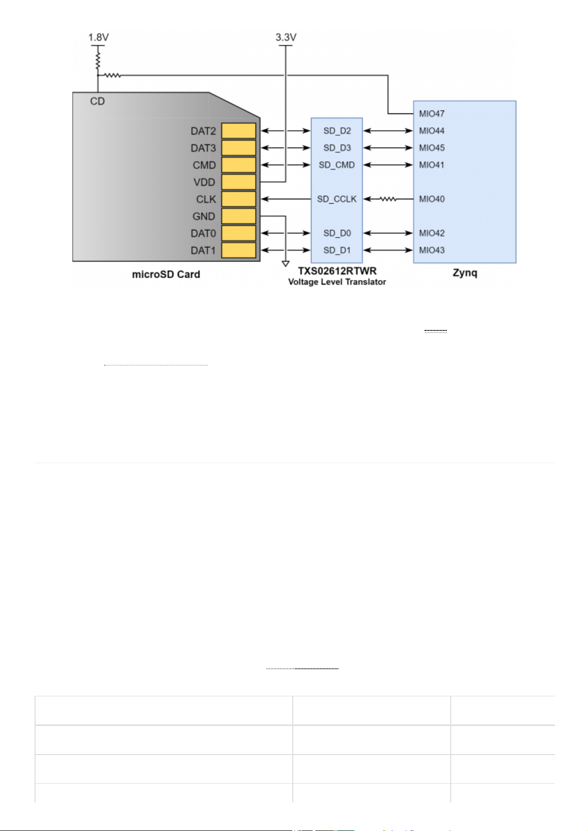
Figure 9.1: microSD slot signals
Both low speed and high speed cards are supported, the maximum clock frequency being 50MHz. A Class 4 card or better
is recommended.
Refer to section2.1 microSD Boot Modefor information on how to boot from a microSD card that contains a Zynq Boot
Image.
The microSD is also commonly used to store non-configuration data needed by the application. If doing this from a baremetal application, the microSD card can be freely accessed using standalone libraries included with a Xilinx SDK BSP
project. If doing this from a Petalinux generated embedded Linux system, the microSD can be mounted/accessed like a
standard block device, typically with a device node named /dev/mmcblk0. See the Petalinux and Xilinx SDK
documentation for more information.
The Eclypse Z7 implements one of the two available PS USB OTG interfaces on the Zynq device. A Microchip USB3320
USB 2.0 Transceiver Chip with an 8-bit ULPI interface is used as the PHY. The PHY features a complete HS-USB Physical
Front-End supporting speeds of up to 480Mbs. The PHY is connected to MIO Bank 1/501, which is powered at 1.8V. The
usb0 peripheral is used on the PS, connected through MIO[28-39]. The USB OTG interface can act as an host, embedded
host, or a peripheral device, through the USB Micro AB connector(J5). The USB mode is controlled from software by
manipulating the USB0 peripheral controller in the Zynq PS.
By default, VBUS capacitance is 4.7 µF. Jumper JP1 may be shorted while in host mode in order to increase VBUS
capacitance by 150 µF. Jumper JP2 must be installed for the Eclypse to power VBUS for host or embedded host
applications. These requirements give three possible configurations for the two jumpers, as presented in Table 10.1.
Whether the Eclypse Z7 is configured as an embedded host or a general purpose host, it can provide at least 500 mA on
the 5V VBUS line. More than 500 mA of current can potentially be provided depending on the system configuration and
how much power is drawn by installed Zmods. See the1 Power Suppliessection for more information.
Table 10.1: USB Mode Jumper Positions
Mode JP1 Shorted JP2 Shorted
Embedded Host No Yes
General Purpose Host Yes Yes
Peripheral Device No No
10. USB Micro-AB Device/Host/OTG Port
Page 21
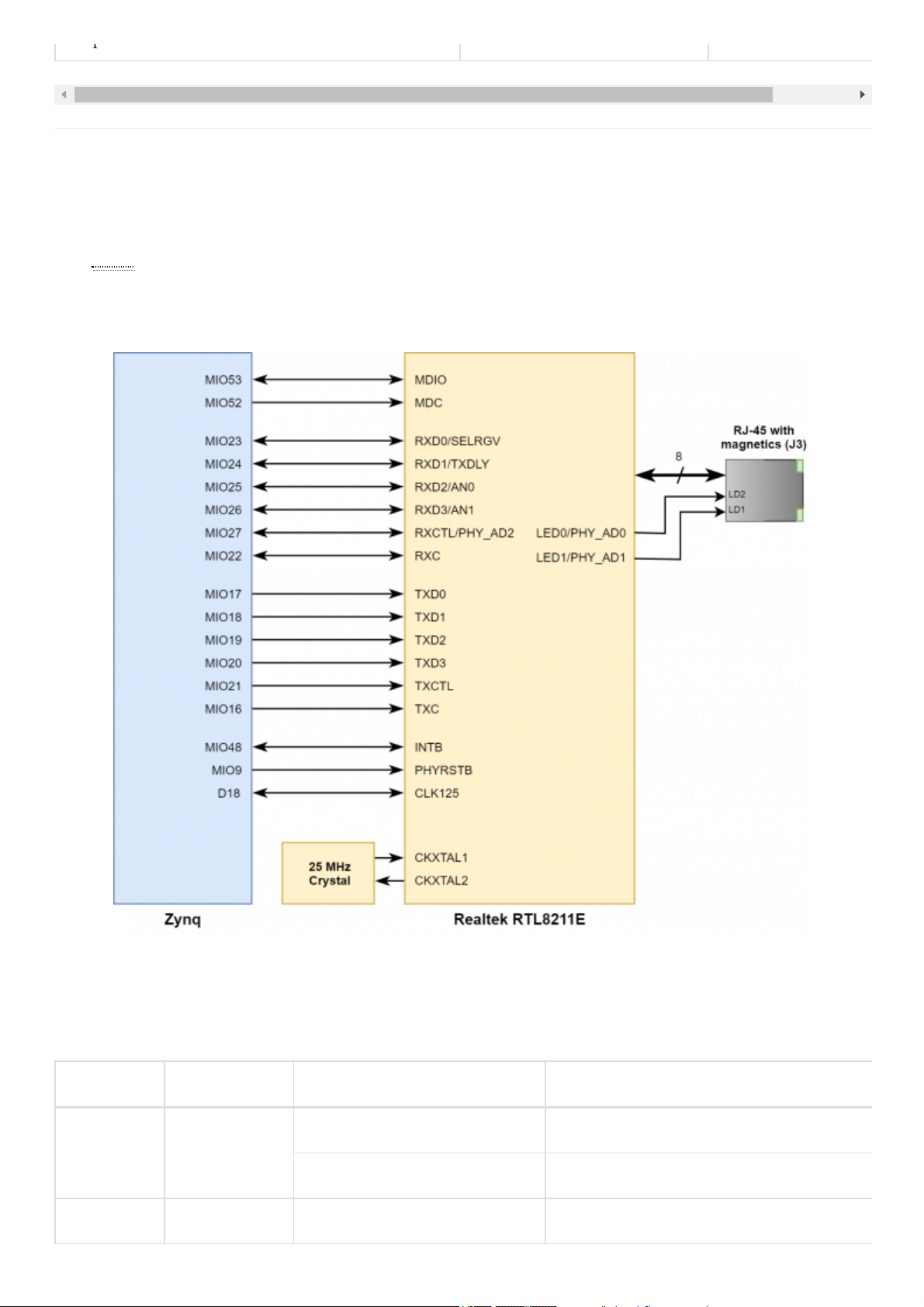
The Eclypse Z7 uses a Realtek RTL8211E-VL PHY to implement a 10/100/1000 Ethernet port for network connection.
The PHY connects to MIO Bank 501 (1.8V) and interfaces to the Zynq-7000 AP SoC via RGMII for data and MDIO for
management. The auxiliary interrupt (INTB) and reset (PHYRSTB) signals connect to PS pins to be accessed through the
MIOGPIOperipheral via MIO48 and MIO9 respectively. The connection diagram can be seen on Figure 11.1.
After power-up the PHY starts with Auto Negotiation enabled, advertising 10/100/1000 link speeds and full duplex. If
there is an Ethernet-capable partner connected, the PHY automatically establishes a link with it, even with the Zynq not
configured.
Figure 11.1: Ethernet PHY signals
Two status indicator LEDs are located on the RJ-45 connector (J3) that indicate traffic (J3/LD2, right side of connector)
and valid link state (J3/LD1, left side of connector). Table 11.1 shows the default behavior.
Table 11.1: Ethernet status LEDs
p
Function Designator State Description
LINK J3/LD1 Steady on Link 10/100/1000
Blinking 0.4s ON, 2s OFF Link, Energy Efficient Ethernet (EEE) mod
ACT J3/LD2 Blinking Transmitting or Receiving
11. Ethernet
Page 22
The Zynq incorporates two independent Gigabit Ethernet Controllers. They implement a 10/100/1000 half/full duplex
Ethernet MAC. Of these two, GEM 0 can be mapped to the MIO pins where the PHY interfaces. Since the MIO bank is
powered from 1.8V, the RGMII interface uses 1.8V HSTL Class 1 drivers. For this I/O standard an external reference of
0.9V is provided in bank 501 (PS_MIO_VREF). Mapping out the correct pins and configuring the interface is handled by
the Eclypse Z7 Vivado board files.
Although the default power-up configuration of the PHY might be enough in most applications, the MDIO bus is available
for management. The RTL8211E-VL is assigned the 5-bit address 00001 on the MDIO bus. With simple register read and
write commands, status information can be read out or configuration changed. The Realtek PHY follows industry-standard
register map for basic configuration.
The RGMII specification calls for the receive (RXC) and transmit clock (TXC) to be delayed relative to the data signals
(RXD[0:3], RXCTL and TXD[0:3], TXCTL). Xilinx PCB guidelines also require this delay to be added. The RTL8211E-VL
is capable of inserting a 2ns delay on both the TXC and RXC so that board traces do not need to be made longer.
On an Ethernet network each node needs a unique MAC address. To this end, the one-time-programmable (OTP) region
of the Quad-SPI flash has been programmed at the factory with a 48-bit globally unique EUI-48/64™ compatible
identifier. The OTP address range [0x20;0x25] contains the identifier with the first byte in transmission byte order being at
the lowest address. Refer to theFlash memory datasheetfor information on how to access the OTP regions. When using
Petalinux, this is automatically handled in the U-boot boot-loader, and the Linux system is automatically configured to use
this unique MAC address. The identifier is also printed on a sticker found on the top-side of the Eclypse Z7 right next to
the mode jumper (JP5) and above the headphone output jack.
For getting started using the ethernet port in a bare-metal application, Xilinx provides a lwip TCP/IP stack that can be
automatically generated in Xilinx SDK along with an echo server example. When using the Eclypse Z7 with a Petalinux
generated embedded Linux system, the ethernet port will automatically appear as a network device typically named eth0.
See the Petalinux and Xilinx SDK documentation for more information.
For more low-level information on using the Zynq-7000 Gigabit Ethernet MAC, refer to the Xilinx Zynq Technical
Reference Manual.
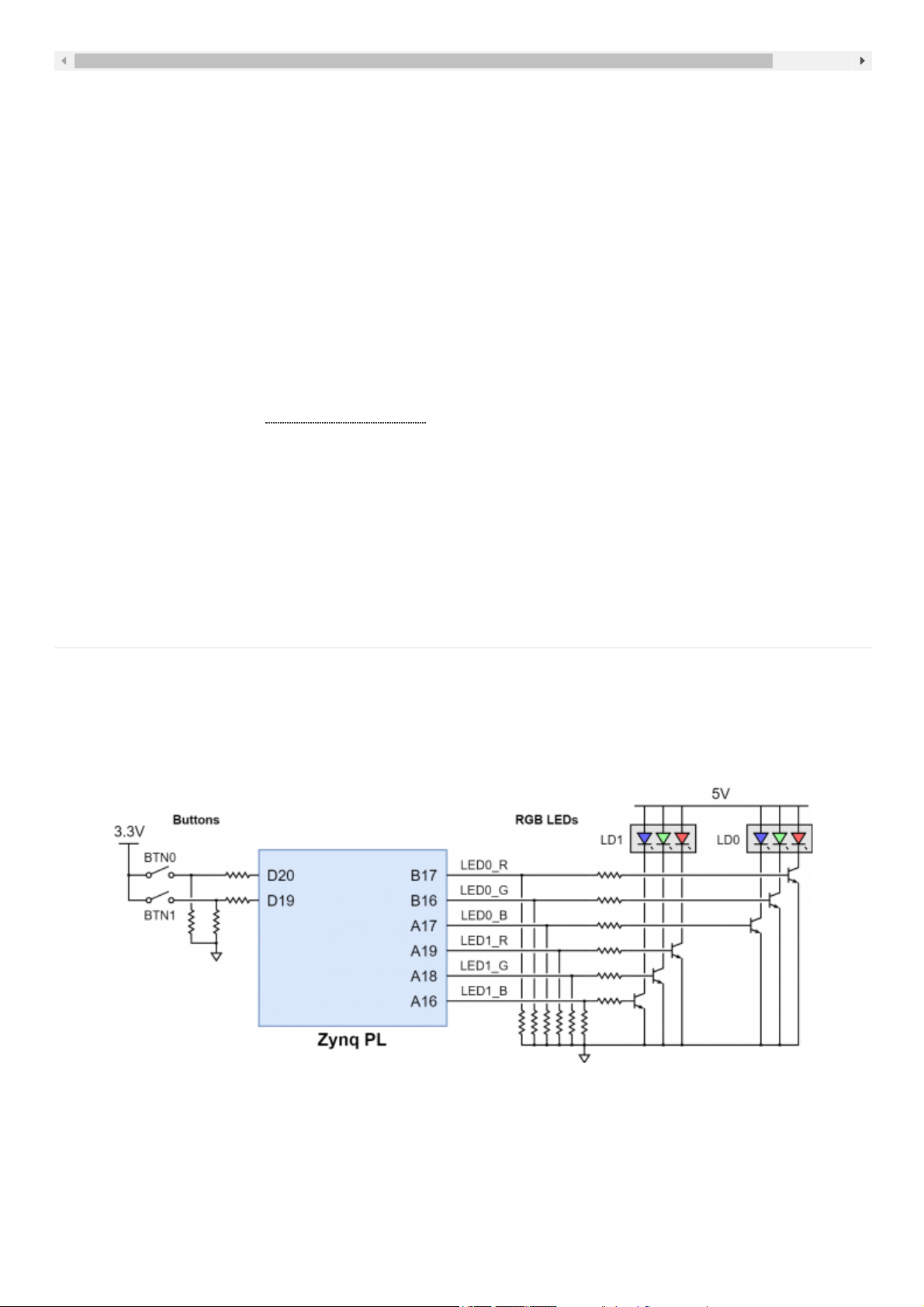
The Eclypse Z7 includes two push-buttons and two tri-color LEDs connected to the Zynq PL, as shown in Figure 12.1.
These I/Os are connected to the Zynq via series resistors to prevent damage from inadvertent short circuits (a short circuit
could occur if a pin assigned to a push-button was inadvertently defined as an output).
Figure 12.1: Eclypse Z7 Basic I/O
The push-buttons are “momentary” switches that normally generate a low output when they are at rest, and a high output
only when they are pressed.
12. Basic I/O
12.1. Push-Buttons
12.2. Tri-Color LEDs
Page 23
Each tri-colorLEDhas three input signals that drive the cathodes of three smaller internal LEDs: one red, one blue, and
one green. Driving the input signal corresponding to one of these colors low will illuminate the internalLED. The input
signals are driven by the Zynq PL through a transistor, which inverts the signals. Therefore, to light up the tri-colorLED,
the corresponding PL pins need to be driven high. The tri-colorLEDwill emit a color dependent on the combination of
internal LEDs that are currently being illuminated. For example, if the red and blue signals are driven high and green is
driven low, the tri-colorLEDwill emit a purple color.
Note:Digilent strongly recommends the use of pulse-width modulation (PWM) when driving the tri-colo LEDs. Driving any of the signals to a
steady logic '1' will result in theLEDbeing illuminated at an uncomfortably bright level. This can be avoided by ensuring that none of the tricolor signals are driven with more than a 50% duty cycle. Using PWM also greatly expands the potential color palette of the tri-colorLED.
Individually adjusting the duty cycle of each color between 0% and 50% causes the different colors to be illuminated at different intensities,
allowing virtually any color to be displayed.
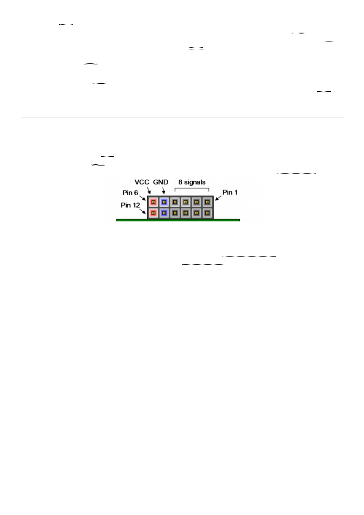
Pmod ports are 2×6, right-angle, 100-mil spaced female connectors that mate with standard 2×6 pin headers. Each 12-pin
Pmod port provides two 3.3VVCCsignals (pins 6 and 12), two Ground signals (pins 5 and 11), and eight logic signals, as
shown in Figure 13.1. TheVCCand Ground pins can deliver up to 1A of current, but care must be taken not to exceed any
of the power budgets of the on-board regulators or the external power supply (as described in thePower suppliessection).
Figure 13.1: Pmod port
Digilent produces a large collection of Pmod accessory boards that can attach to the Pmod ports to add ready-made
functions like A/D’s, D/A’s, motor drivers, sensors, and other functions. Seewww.digilentinc.comfor more information.
The vivado-library and vivado-hierarchies repositories on theDigilent Githubcontains pre-made IP cores for many of
these Pmods that greatly reduces the work of integrating them into your project. See the Pmod-related tutorials on the
Eclypse Z7 Resource Center for help using them.
The Eclypse Z7's two Pmod ports are connected to the Zynq PL via high-speed down translation and protection circuitry.
When used as outputs, the Pmod pins are driven at 3.3V. When used as inputs, the Pmod pins are 5V tolerant. The
maximum recommended voltage applied to these pins is 5.5V, though the inline resettable fuses will protect the FPGA pins
from damage.
13. Pmod Ports
 Loading...