

Page 1

The Digilent Pmod CMPS2 (Revision A) is a 3-axis anisotropic magneto-resistive sensor. WithMemsic's MMC34160PJ, the
local magnetic field strength in a ±16 Gauss range with a heading accuracy of 1° and up to 0.5 mG of resolution.
Pmod CMPS2 Reference Manual
Page 2

Page 3

Page 4

Page 5

Pmod CMPS2 PDF
Low noise 3-axis Digital Compass
0.5 mG Field Resolution in ±16 Gauss fields
I²C Slave, FAST (≤400kHz) mode
Optional pull-up resistors for SCL and SDA pins
±1° heading accuracy
Small PCB size for flexible designs 0.8“ × 1.25” (2.0 cm × 3.2 cm)
6-pin Pmod connector with I²C serial interface
Pass-through Pmod host port for daisy chaining
Follows DigilentPmod Interface Specification 1.1.0
Library and example code in the Pmod CMPS2Resource Center
Parameter Min Typical Max
Power Supply Voltage 1.62 1.8 3.6
Download This Reference Manual
Features
Specifications
Page 6

Parameter Min Typical Max
Output Resolution 12 14 16
Alignment Error -3 ±1 +3
Parameter Condition Value
Total RMS Noise 16 bits at 7.92 ms/S 1.5
Total RMS Noise 16 bits at 4.08 ms/S 2.0
Total RMS Noise 14 bits at 2.16 ms/S 4.0
Total RMS Noise 12 bits at 1.20 ms/S 6.0
Max Output Data Rate 16 bits at 7.92 ms/S 125
Max Output Data Rate 16 bits at 4.08/S 250
Max Output Data Rate 14 bits at 2.16 ms/S 450
Max Output Data Rate 12 bits at 1.20 ms/S 800
Parameter Value
Field Range for Each Axis ±16
Header J1 Header J2 Jumper JP1
Pin Signal Description Pin Signal Description Pin Status Desc
1 N/C Not Connected 1 N/C Not Connected SCL Loaded 4.7 kΩ
V
2 N/C Not Connected 2 N/C Not Connected SCL Unloaded No Pullu
3 SCL Serial Clock 3 SCL Serial Clock SDA Loaded 4.7 kΩ
V
4 SDA Serial Data 4 SDA Serial Data SDA Unloaded No Pullu
5 GND Power Supply
Ground
5 GND Power Supply
Ground
6 VCC Power Supply (3.3V) 6 VCC Power Supply (3.3V)
Pinout Table Diagram
Page 7

The pins on the pin header are spaced 100 mil apart. The PCB is 1.25 inches long on the sides parallel to the pins on the
pin header and 0.8 inches long on the sides perpendicular to the pin header.
The Pmod CMPS2 utilizes the MMC34160PJ to collect magnetic field data. While communicating with the host board via
theI²C protocolusing an I²C address of 0x0110000/ users can measure the ±16 G field surrounding the device.
The Pmod CMPS2 communicates with the host board via theI²C protocol. By first sending the 7-bit I²C device address of
0110000 and then a read/write bit (high/low logic level, respectively), followed by the register address of interest at a
maximum clock frequency of 400kHzusers can both configure and read from the Pmod CMPS2. An additional set of pins
on header J2 is provided so that users may daisy chain the Pmod CMPS2 with other I²C devices.
Each Cartesian axis has two registers to store the high and low data bytes for each measurement. The data registers are
arranged in a low byte, high byte arrangement.
Data Registers addresses 0x00 to 0x05
Address Register Name
0x00 X out LSB
0x01 X out MSB
0x02 Y out LSB
0x03 Y out MSB
0x04 Z out LSB
0x05 Z out MSB
Bit Name
Bit
Number
Bit
Description
Bit
Values Functional Description
RSV [7] Reserved 0¹ Reserved Bit
RSV [6] Reserved 0¹ Reserved Bit
RSV [5] Reserved 0¹ Reserved Bit
Physical Dimensions
Functional Description
Serial Communication
Register Details
Data Registers
Status Register
Page 8

Bit Name
Bit
Number
Bit
Description
Bit
Values Functional Description
RSV [4] Reserved 0¹ Reserved Bit
ST_XYZ_OK [3] ST_XYZ_OK 0¹ Indicates that the selftest was OK when this bi
Rd_Done [2] Rd_Done 0¹ Indicates that chip was successfully able to read
memory.
Pump On [1] Pump On 0¹ This bit indicates the status of the charge pump
RSV [0] Meas Done 0¹ Indicates that a measurement event is complete
Internal Control 0 Internal Control 1
Bit
Name
Bit
Number
Bit
Description
Bit
Values
Functional
Description
Bit
Name
Bit
Number
Bit
Description
Bit
Valu
Refill
Cap
[7] Refill Cap 0¹ Setting this
bit will
recharge the
capacitor at
the CAP pin,
it is
requested to
be issued
before the
SET/RESET
command
RST [7] Software
reset bit
0¹
RST [6] Reset Sensor 0¹ Setting this
bit will reset
the sensor
TEMPtst
[6] Temp test 0¹
SET [5] Set Sensor 0¹ Setting this
bit will set
the sensor
ST_XYZ [5] Selftest
check
0¹
Internal Control Registers
Page 9

Notes:
¹ - This is the value on power-up and reset
² - For more details see theContinuous Measurement Modesection
³ - For more details see theOutput Resolution and Measurement Timesection
Internal Control 0 Internal Control 1
Bit
Name
Bit
Number
Bit
Description
Bit
Values
Functional
Description
Bit
Name
Bit
Number
Bit
Description
Bit
Valu
No
Boost
[4] No boost 0¹ Disable the
charge pump
Z-inhibit [4] Z-inhibit 0¹
CM
Freq1²
[3] Continuous
Measurement
bit 1
0¹ Controls the
continuous
measurement
rate of the
chip
Y-inhibit [3] Y-inhibit 0¹
CM
Freq0²
[2] Continuous
Measurement
bit 0
0¹ Controls the
continuous
measurement
rate of the
chip
X-inhibit [2] X-inhibit 0¹
Cont
Mode
On
[1] Continuous
Measurement
Mode
0¹ Setting this
bit enables
Continuous
Measurement
Mode
BW1³ [1] Bandwidth
bit
0¹
TM [0] Take
Measurement
0¹ Setting this
bit will
initiate a
reading
BW0³ [0] Bandwidth
bit
0¹
Continuous Measurement Mode Settings
CM Freq1 CM Freq0 Frequency
0 0 1.5Hz
0 1 13Hz
Continuous Measurement Mode
Page 10

Here is the series of commands to acquire a set of magnetometer data from the Pmod CMPS2 via pseudo I²C code.
1. Power on the Pmod CMPS2 and wait for 10 mS before further operation.
2. Provide a START condition and call the device ID with a write bit
I2CBegin(0xA0); //device ID 0x30 with a write (0) bit
3. Wait to receive an ACK from the Pmod CMPS2.
4. Send the Internal Control Register 0 (address 0x07) as the register to communicate with
I2CWrite(0x07); //address 0x07 corresponds to Control Register 0
5. Wait to receive an ACK from the Pmod CMPS2.
6. Write the command to take a measurement by setting bit 0 high followed by a STOP bit.
I2CWrite(0x01); //0x01 initiates a data acquisition
7. Delay at least 7.92 mS by default to allow the Pmod CMPS2 to finish collecting data.
8. Provide a START condition and call the device ID with a write bit
I2CBegin(0xA0); //device ID 0x30 with a write (0) bit
9. Wait to receive an ACK from the Pmod CMPS2.
10. Send the Status Register (0x03) as the register to read
I2CWrite(0x03); //indicate you wish to interact with address 0x03
11. Provide a START condition and call the device ID with a read bit
Continuous Measurement Mode Settings
CM Freq1 CM Freq0 Frequency
1 0 25Hz
1 1 50Hz
Bandwidth Output Resolution and Measurement Time
BW1 BW0 Output Resolution Measurement Time
0 0 16 bits 7.92 mS
0 1 16 bits 4.08 mS
1 0 14 bits 2.16 mS
1 1 12 bits 1.20 mS
Output Resolution and Measurement Time
Quick Start
Page 11

I2CBegin(0xA1); //device ID 0x30 with a read (1) bit
12. Wait to receive an ACK from the Pmod CMPS2.
13. Cycle the SCL line to receive the Status Register data on the SDA line. Keep reading the Status Register by repeating
steps 8 through 13 until bit 0 is set to '1', indicating that the data on all 3 axes as available to be read.
14. Provide a START condition and call the device ID with a write bit
I2CBegin(0xA0); //device ID 0x30 with a write (0) bit
15. Wait to receive an ACK from the Pmod CMPS2.
16. Send the first register address corresponding to Xout LSB (0x00) as the register to be read.
I2CWrite(0x00); //address 0x00 as the first register to be read
17. Provide a START condition and call the device ID with a read bit
I2CBegin(0xA1); //device ID 0x30 with a read (1) bit
18. Wait to receive an ACK from the Pmod CMPS2.
19. Cycle the SCL line to receive the data bits from the X, Y, and Z registers in the SDA line, providing an ACK
between each data byte. The Pmod CMPS2 address pointer automatically moves to each consecutive byte. End the
communication by sending a NACK followed by a STOP command.
20. Convert the readings into usable data. More details are available in the Data Conversion section.
21. Wait 1/3 of the acquisition time (by default 2.64 ms) before performing another measurement.
The Pmod CMPS2 is an ideal Pmod to use as a compass. Like all compasses, it is recommended that the Pmod CMPS2 is
calibrated before using the module.
To calibrate the magnetometer, the offset associated with the magnetic sensors and the environment needs to be calculated
and removed from future measurements.
The internal offset can be calculated and accounted for through the following method:
Reveal the Method
1. Power on the Pmod CMPS2 and wait for 10 mS before further operation.
2. Provide a START condition and call the device ID with a write bit
I2CBegin(0xA0); //device ID 0x30 with a write (0) bit
3. Wait to receive an ACK from the Pmod CMPS2.
4. Send the Internal Control Register 0 (address 0x07) as the register to communicate with
I2CWrite(0x07); //address 0x07 corresponds to Control Register 0
5. Wait to receive an ACK from the Pmod CMPS2.
6. Write the command to recharge the capacitor to prepare for the SET action.
I2CWrite(0x80); //0x80 refills the capacitor
7. Wait to receive an ACK from the Pmod CMPS2.
8. Delay at least 50 mS to allow the Pmod CMPS2 to finish preparing.
9. Provide a START condition and call the device ID with a write bit
I2CReadMultiple(6); //read six bytes, sending an ACK to the slave device between each byte
Applications Information
Calibration
Page 12

I2CBegin(0xA0); //device ID 0x30 with a write (0) bit
10. Wait to receive an ACK from the Pmod CMPS2.
11. Send the Internal Control Register 0 (address 0x07) as the register to communicate with
I2CWrite(0x07); //address 0x07 corresponds to Control Register 0
12. Wait to receive an ACK from the Pmod CMPS2.
13. Write the command to start a SET action.
I2CWrite(0x20); //0x20 starts the SET action
14. Wait to receive an ACK from the Pmod CMPS2.
15. Delay at least 1 mS to allow the Pmod CMPS2 to finish the SET action.
16. Provide a START condition and call the device ID with a write bit
I2CBegin(0xA0); //device ID 0x30 with a write (0) bit
17. Wait to receive an ACK from the Pmod CMPS2.
18. Send the Internal Control Register 0 (address 0x07) as the register to communicate with
I2CWrite(0x07); //address 0x07 corresponds to Control Register 0
19. Wait to receive an ACK from the Pmod CMPS2.
20. Write the command to take a measurement by setting bit 0 high followed by a STOP bit.
I2CWrite(0x01); //0x01 initiates a data acquisition
21. Delay at least 7.92 mS by default to allow the Pmod CMPS2 to finish collecting data.
22. Provide a START condition and call the device ID with a write bit
I2CBegin(0xA0); //device ID 0x30 with a write (0) bit
23. Wait to receive an ACK from the Pmod CMPS2.
24. Send the Status Register (0x03) as the register to read
I2CWrite(0x03); //indicate you wish to interact with address 0x03
25. Provide a START condition and call the device ID with a read bit
I2CBegin(0xA1); //device ID 0x30 with a read (1) bit
26. Wait to receive an ACK from the Pmod CMPS2.
27. Cycle the SCL line to receive the Status Register data on the SDA line. Keep reading the Status Register by repeating
steps 8 through 13 until bit 0 is set to '1', indicating that the data on all 3 axes as available to be read.
28. Provide a START condition and call the device ID with a write bit
I2CBegin(0xA0); //device ID 0x30 with a write (0) bit
29. Wait to receive an ACK from the Pmod CMPS2.
30. Send the first register address corresponding to Xout LSB (0x00) as the register to be read.
I2CWrite(0x00); //address 0x00 as the first register to be read
31. Provide a START condition and call the device ID with a read bit
I2CBegin(0xA1); //device ID 0x30 with a read (1) bit
Page 13

32. Wait to receive an ACK from the Pmod CMPS2.
33. Cycle the SCL line to receive the data bits from the X, Y, and Z registers in the SDA line, providing an ACK
between each data byte. The Pmod CMPS2 address pointer automatically moves to each consecutive byte. End the
communication by sending a NACK followed by a STOP command.
34. Each of the readings will contain the external magnetic fieldHin addition to offset associated with the current put
through the coil by the SET action.
35. Now a RESET action will be performed to reverse the magnetization for the sensing resistors to get the inverse
offset value.
36. Provide a START condition and call the device ID with a write bit
I2CBegin(0xA0); //device ID 0x30 with a write (0) bit
37. Wait to receive an ACK from the Pmod CMPS2.
38. Send the Internal Control Register 0 (address 0x07) as the register to communicate with
I2CWrite(0x07); //address 0x07 corresponds to Control Register 0
39. Wait to receive an ACK from the Pmod CMPS2.
40. Write the command to recharge the capacitor to prepare for the RESET action.
I2CWrite(0x80); //0x80 refills the capacitor
41. Wait to receive an ACK from the Pmod CMPS2.
42. Delay at least 50 mS to allow the Pmod CMPS2 to finish preparing.
43. Provide a START condition and call the device ID with a write bit
I2CBegin(0xA0); //device ID 0x30 with a write (0) bit
44. Wait to receive an ACK from the Pmod CMPS2.
45. Send the Internal Control Register 0 (address 0x07) as the register to communicate with
I2CWrite(0x07); //address 0x07 corresponds to Control Register 0
46. Wait to receive an ACK from the Pmod CMPS2.
47. Write the command to start a RESET action.
I2CWrite(0x40); //0x40 starts the RESET action
48. Wait to receive an ACK from the Pmod CMPS2.
49. Delay at least 1 mS to allow the Pmod CMPS2 to finish the SET action.
50. Provide a START condition and call the device ID with a write bit
I2CBegin(0xA0); //device ID 0x30 with a write (0) bit
51. Wait to receive an ACK from the Pmod CMPS2.
52. Send the Internal Control Register 0 (address 0x07) as the register to communicate with
I2CWrite(0x07); //address 0x07 corresponds to Control Register 0
53. Wait to receive an ACK from the Pmod CMPS2.
54. Write the command to take a measurement by setting bit 0 high followed by a STOP bit.
I2CReadMultiple(6); //read six bytes, sending an ACK to the slave device between each byte
Output1 = +H + Offset
Page 14

I2CWrite(0x01); //0x01 initiates a data acquisition
55. Delay at least 7.92 mS by default to allow the Pmod CMPS2 to finish collecting data.
56. Provide a START condition and call the device ID with a write bit
I2CBegin(0xA0); //device ID 0x30 with a write (0) bit
57. Wait to receive an ACK from the Pmod CMPS2.
58. Send the Status Register (0x03) as the register to read
I2CWrite(0x03); //indicate you wish to interact with address 0x03
59. Provide a START condition and call the device ID with a read bit
I2CBegin(0xA1); //device ID 0x30 with a read (1) bit
60. Wait to receive an ACK from the Pmod CMPS2.
61. Cycle the SCL line to receive the Status Register data on the SDA line. Keep reading the Status Register by repeating
steps 8 through 13 until bit 0 is set to '1', indicating that the data on all 3 axes as available to be read.
62. Provide a START condition and call the device ID with a write bit
I2CBegin(0xA0); //device ID 0x30 with a write (0) bit
63. Wait to receive an ACK from the Pmod CMPS2.
64. Send the first register address corresponding to Xout LSB (0x00) as the register to be read.
I2CWrite(0x00); //address 0x00 as the first register to be read
65. Provide a START condition and call the device ID with a read bit
I2CBegin(0xA1); //device ID 0x30 with a read (1) bit
66. Wait to receive an ACK from the Pmod CMPS2.
67. Cycle the SCL line to receive the data bits from the X, Y, and Z registers in the SDA line, providing an ACK
between each data byte. The Pmod CMPS2 address pointer automatically moves to each consecutive byte. End the
communication by sending a NACK followed by a STOP command.
68. Each of the readings will contain the external magnetic fieldHin addition to offset associated with the current put
through the coil by the RESET action.
69. The offset associated with the device can be calculated and then subtracted from future measurements to obtain the
actual magnetic field.
The other method of calibration is to remove the hard iron bias introduced to the magnetometer by the surrounding
environment by measuring (either continually or for a set time) all of the possible magnetometer readings in a Cartesian
sphere and keep track of the highest and lowest readings for each axis. The offset can then be calculated in the same
fashion as described above with the SET and RESET actions. The advantage of this method is when the Pmod CMPS2 is
continually changing locations or when other external magnetic fields may be introduced into the test environment.
The Memsic MMC34160PJ provides data for each axis in units of Gauss, but the information is generally more legible
when presented as a compass heading. The method for converting Gauss units to a compass heading is provided below.
I2CReadMultiple(6); //read six bytes, sending an ACK to the slave device between each byte
Output2 = −H + Offset
Offset =
Output1 + Output2
2
Data Conversion
Page 15
Reveal the Method
1. Calculate the real Gauss value for the X and Y axes from the amount of LSBs returned where the LSB value by
default is 0.48828125 mG, resulting in 2048 LSBs per Gauss.
2. Calculate the directionDby first checking to see if the X Gauss data is equal to 0 to prevent divide by 0 zero errors
in the future calculations. If the X Gauss data is 0, check to see if the Y Gauss data is less than 0. If Y is less than 0
Gauss, the direction D is 90 degrees; if Y is greater than or equal to 0 Gauss, the direction D is 0 degrees.
3. If the X Gauss data is not zero, calculate the arctangent of the Y Gauss and X Gauss data and convert from polar
coordinates to degrees.
4. If the direction D is greater than 360 degrees, subtract 360 degrees from that value.
5. If the direction D is less than 0 degrees, add 360 degrees to that value.
6. The compass heading can then be determined by the direction value D:
If D is greater than 337.25 degrees or less than 22.5 degrees – North
If D is between 292.5 degrees and 337.25 degrees – North-West
If D is between 247.5 degrees and 292.5 degrees – West
If D is between 202.5 degrees and 247.5 degrees – South-West
If D is between 157.5 degrees and 202.5 degrees – South
If D is between 112.5 degrees and 157.5 degrees – South-East
If D is between 67.5 degrees and 112.5 degrees – East
If D is between 0 degrees and 67.5 degrees – North-East
←-
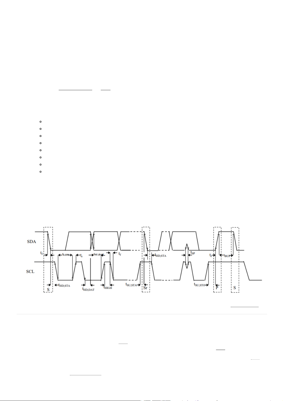
An example timing diagram for reading and writing to the Pmod CMPS2 taken from the Memsic datasheet is provided
below:
When using an external power supply to run the Pmod, be sure to stay within the parameters provided inSpecifications.
The schematics of the Pmod CMPS2 are availablehere. Additional information about the humidity sensor including
communication modes and specific timings of the chip can be found by checking out its datasheethere.
Example code demonstrating how to get information from the Pmod CMPS2 can be found on its Resource Centerhere.
If you have any questions or comments about the Pmod CMPS2, feel free to post them under the appropriate section
(“Add-on Boards”) of theDigilent Forum.
xGaussData = xDataLSB ∗ 0.48828125 mG
yGaussData = yDataLSB ∗ 0.48828125 mG
D = arctan ( ) ∗
yGaussData
xGaussData
180
π
Timing Diagrams
Additional Information
 Loading...