

Page 1

Opus Card – DDR-2 Interface
Reference Manual
Revision Name Date
0.02 Rick Hoover August 21, 2009
0.03 Rick Hoover – Added support for burst reads and writes September 30, 2009
0.04 Rick Hoover – Made corrections to Bus2IP_RdReq that
match ChipScope traces. Basically Bus2IP_RdReq is
active for only one clock on non-burst reads and is active
one additional clock past the de-assertion of Bus2IP_CS
for burst reads.
0.10 Rick Hoover – Added support for burst of eight quadwords. This is required for DMA accesses. Also added
configuration register for resetting the Ethernet PHY and to
control burst accesses via software.
1.00 Rick Hoover – Released December 3, 2010
Copyright © 2009-2010 by Computer Measurement Laboratory, LLC
October 6, 2009
November 16, 2009
12/03/2010 07:35 AM 1
Copyright © 2009-2010 by CML
Page 2

Opus Card – DDR-2 Interface
Reference Manual
Table of Contents
1. INTRODUCTION ..................................................................................................................................................3
1.1 DEBUG REGISTERS ACCESSIBLE BY THE CPU .....................................................................................................3
1.2 CONFIGURATION REGISTER ACCESSIBLE BY THE CPU........................................................................................3
1.3 ENDIANNESS........................................................................................................................................................3
1.4 DDR-2 MEMORY ACCESSIBLE BY THE CPU .......................................................................................................4
2. STATE MACHINE FOR WRITING DATA TO MEMORY.............................................................................5
2.1 SIGNAL DEFINITIONS...........................................................................................................................................5
2.2 WRITE STATE MACHINE......................................................................................................................................6
2.3 WAVEFORMS .......................................................................................................................................................7
2.3.1 Non-burst, 32-bit Memory Write .................................................................................................................7
2.3.2 Non-burst, 64-bit Memory Write .................................................................................................................8
2.3.3 Burst Memory Write - Four 32-bit Words ...................................................................................................9
2.3.4 Burst Memory Write - Eight 32-bit Words.................................................................................................10
2.3.5 Burst Memory Write – Two 64-bit Words..................................................................................................11
2.3.6 Burst Memory Write - Four 64-bit Words .................................................................................................12
3. STATE MACHINES FOR READING DATA FROM MEMORY..................................................................13
3.1 SIGNAL DEFINITIONS.........................................................................................................................................13
3.2 READ STATE MACHINE .....................................................................................................................................14
3.2 READ FIFO STATE MACHINE ............................................................................................................................15
3.3 WAVEFORMS .....................................................................................................................................................16
3.3.1 Non-burst, 32-bit Memory Read Clock-Aligned ........................................................................................16
3.3.2 Non-burst, 32-bit Memory Read not Clock-Aligned ..................................................................................17
3.3.3 Non-burst, 64-bit Memory Read................................................................................................................18
3.3.4 Burst Memory Read - Four 32-bit Words..................................................................................................19
3.3.5 Burst Memory Read - Eight 32-bit Words .................................................................................................20
3.3.6 Burst Memory Read - Two 64-bit Words ...................................................................................................21
3.3.7 Burst Memory Read - Four 64-bit Words..................................................................................................22
12/03/2010 07:35 AM 2
Copyright © 2009-2010 by CML
Page 3

Opus Card – DDR-2 Interface
Reference Manual
1. Introduction
This document provides the details on how DDR-2 memory on the Opus card is connected into
the PLB bus contained in the Xilinx Virtex-5 FPGA using the Embedded Design Kit (EDK).
The CML team discovered that the default Multi-Port Memory Controller (MPMC) provided
with the EDK had problems which reduced the reliability of accessing the DDR-2 memory
contained on the Opus card.
For additional details on many of the registers described here, see document DS562 from Xilinx.
This Xilinx document is titled “PLBV46 Slave Burst”. In addition, there are further details on
the DDR-2 memory controller generated using Xilinx MIG in document UG086 that is titled
“Memory Interface Solutions User Guide”.
1.1 Debug Registers Accessible by the CPU
There are several debug registers that can be read via the CPU to determine the calibrated state
of the DDR-2 PHY. These registers are detailed below:
• 0x84800000 – DQ IODELAY settings for bits 3 downto 0
• 0x84800004 – DQ IODELAY settings for bits 7 downto 4
• 0x84800008 – DQ IODELAY settings for bits 11 downto 8
• 0x8480000C – DQ IODELAY settings for bits 15 downto 12
• 0x84800010 – DQ IODELAY settings for bits 19 downto 16
• 0x84800014 – DQ IODELAY settings for bits 23 downto 20
• 0x84800018 – DQ IODELAY settings for bits 27 downto 24
• 0x8480001C – DQ IODELAY settings for bits 31 downto 28
• 0x84800020 – DQS IODELAY settings
• 0x84800024 – Gate Tap IODELAY settings
• 0x84800028 – Read Data Enable (RDEn) delay and Data Select IODELAY settings
• 0x8480002C – Gate delay settings
1.2 Configuration Register Accessible by the CPU
There is one configuration register that can be set via the CPU. This configuration register
controls the reset of the external Ethernet PHY and memory burst accesses. In big endian
format, bit 30 resets the Ethernet PHY when set to ‘1’ and bit 31 enables burst mode when set to
‘1’. Besides a hardware reset, the only way to clear these bits is by a write to the configuration
register. So, it is important to clear bit 30 by a write to the configuration register after the
required 100uS have elapsed to bring the Ethernet PHY out of reset mode.
1.3 Endianness
The PLB slave assumes a big endian interface to memory. Therefore, memory is organized in a
big endian fashion where byte 0 is in bits 0 to 7, byte 1 is in bits 8 to 15 and so forth where bit 0
is the most significant bit in a word.
12/03/2010 07:35 AM 3
Copyright © 2009-2010 by CML
Page 4

Opus Card – DDR-2 Interface
Reference Manual
1.4 DDR-2 Memory Accessible by the CPU
The DDR-2 memory is 128 MBytes in size, organized as 32-bit words. The memory is
accessible from 0x88000000 to 0x8FFFFFFF.
The C_CACHLINE_ADDR_MODE for the PLB interface in the DDR-2 memory controller
MUST be set to 1 so that cache line bursts always start at the first address in the cache line. A
setting of 0, which is the default, will not work with the current implementation of the DDR-2
memory controller.
12/03/2010 07:35 AM 4
Copyright © 2009-2010 by CML
Page 5

Opus Card – DDR-2 Interface
Reference Manual
2. State Machine for Writing Data to Memory
This chapter covers the state machine that controls the writing of data sent via the PLB bus to the
DDR-2 Memory Controller. The write state machine supports both non-burst writes and burst
writes. Burst writes are limited to a multiple of four 32-bit words or a multiple of two 64-bit
words depending on the width of the PLB data bus and should be limited to a maximum length
of eight quad-words (128 bytes). Each burst is assumed to have consecutive addresses starting
with an address masked by 0xFFFFFFF0. Burst writes also assume that all bytes in the burst are
to be written (i.e. bus2IP_BE is all 1’s).
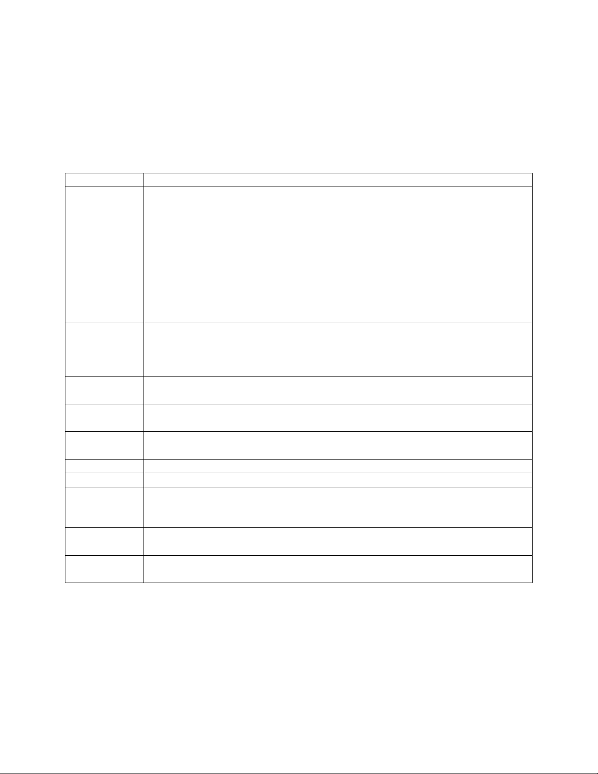
2.1 Signal Definitions
The table below provides details on the signals used for writing data to memory.
Name I/O Description
Bus2IP_Clk I The clock for the PLB bus (currently 100 MHz)
DDR2_Clk I The clock for the DDR-2 memory (currently 200 MHz)
Bus2IP_Reset I Reset signal for the block
App_AF_AFull I Indicates the DDR-2 address buffer is full – not currently used
App_WDF_AFull I Indicates the DDR-2 data buffer is full – not currently used
Bus2IP_Addr I Address of memory to write to
Bus2IP_CS I Indicates the DDR-2 memory is being accessed
Bus2IP_Burst I Indicates a burst read or write is occurring
Bus2IP_RNW I Indicates a write access when low
Bus2IP_WrReq I Indicates a write request
Bus2IP_BE I Indicates bytes to write to (big endian format)
Bus2IP_Data I Data to be written to memory
Rd_Send_Ack I Indicates the read from the PLB slave should be acknowledged
on the next clock cycle.
Rd_Send_Cmd I Indicates the read command and address should be sent to the
DDR-2 memory controller on the next clock cycle.
App_AF_WREn O Causes a write to the DDR-2 address buffer on the rising edge
of DDR2_Clk
App_WDF_WREn O Causes a write to the DDR-2 data buffer on the rising edge of
DDR2_Clk – must write enough data for four consecutive
addresses
App_AF_Cmd O The command to be written to the DDR-2 controller (a Write
command)
App_AF_Addr O The first address that is written to in the DDR-2 memory
App_WDF_Data O The data to be written to the DDR-2 memory
App_WDF_Mask_Data O The mask for the data being writing to the DDR-2 controller
(big endian format)
IP2Bus_RdAck O Acknowledges that the read to memory has occurred
IP2Bus_WrAck O Acknowledges that the write to memory has occurred
IP2Bus_AddrAck O Acknowledges that the address to write to has been latched
12/03/2010 07:35 AM 5
Copyright © 2009-2010 by CML
Page 6
Opus Card – DDR-2 Interface
Reference Manual
2.2 Write State Machine
The write state machine currently has ten states to support the writing of data to memory.
Transitions from one state to the next occur on the rising edge of DDR2_Clk and the state
machine is synchronously reset to Idle when Bus2IP_Reset is ‘1’. Each state is described below:
State Description
Idle Waiting for a write from the PLB slave. A write is detected when Bus2IP_CS is
‘1’, Bus2IP_RNW is ‘0’, App_AF_AFull is ‘0’, and App_WDF_Afull is ‘0’.
The state machine transitions to Wait_Wr_Req on the next clock when these
conditions are met.
This state is also used to pass through needed commands from the read_ctrl
entitiy. The read_ctrl entity generates the Rd_Send_Ack and Rd_Send_Cmd
signals that are used to control the App_AF_Cmd, App_AF_Addr,
App_AF_WREn, IP2Bus_AddrAck, and IP2Bus_RdAck outputs when in this
state.
Wait_Wr_Req Waiting for Bus2IP_WrReq to transition to ‘1’ to indicate the data to be written
to memory is valid. The state machine transitions to the next state when
Bus2IP_WrReq is ‘1’. The next state is Wr_Word1 if Bus2IP_Burst is ‘0’.
Otherwise the next state is Save_W1.
Save_W1 Save word 1 of burst write. The next state is Wr_Word1 when the PLB slave is
configured for 64-bit data width. Otherwise the next state is Save_W2.
Save_W2 Save word 2 of burst write (32-bit PLB bus only). When Bus2IP_Clk is ‘0’, the
next state is set to Save_W3.
Save_W3 Save word 3 of burst write (32-bit PLB bus only). ). When Bus2IP_Clk is ‘0’,
the next state is set to Wr_Brst1.
Wr_Brst1 Write word 1 of burst to DDR-2. The next state is Wr_Brst2.
Wr_Brst2 Write word 2 of burst to DDR-2. The next state is Wr_BrstD.
Wr_BrstD Delay after burst write to DDR-2. The next state is Save_W1 if the burst write
is not complete (Bus2IP_Burst = ‘1’ and Bus2IP_CS = ‘1’). Otherwise the next
state is Idle.
Wr_Word1 State that writes the low order 64-bit word to memory. The state machine
transitions to Wr_Word2 on the next clock.
Wr_Word2 State that writes the high order 64-bit word to memory. The state machine
transitions to Idle on the next clock.
12/03/2010 07:35 AM 6
Copyright © 2009-2010 by CML
Page 7
Opus Card – DDR-2 Interface
Reference Manual
2.3 Waveforms
2.3.1 Non-burst, 32-bit Memory Write
The diagram below is for a non-burst memory write to a single 32-bit word. The Bus2IP_BE bus
is used to determine which bytes to write in the 32-bit word. The use of the Bus2IP_BE bus
enables the hardware controlling the PLB slave to also write eight or sixteen bit values to a 32bit memory location.
1 2 3 4 5 6 7 8 9 10 11
DDR2_ Clk
Bus2IP_Clk
Bus2IP_CS
Bus2IP_RNW
Bus2IP_Addr
Bus2IP_BE
Bus2IP_WrReq
Bus2IP_Data
IP2Bus_AddrAck
IP2Bus_WrAck
App_AF_WREn
App_AF_Cmd
App_AF_Addr
App_WDF_WREn
App_WDF_Data
App_WDF_Mask_Data
Stat e
Addre ss
Byte Enab les
32-bi t Data
Wr i t e
Address
Wo r d 1 Wo r d 2
Mask1 Mask2
Idle Wait_WrReq Wr_Word1 Wr_Word2 Idle
TimeGen
12/03/2010 07:35 AM 7
Copyright © 2009-2010 by CML
Page 8

Opus Card – DDR-2 Interface
Reference Manual
2.3.2 Non-burst, 64-bit Memory Write
The diagram below is for a non-burst memory write to a single 64-bit word. The Bus2IP_BE bus
is used to determine which bytes to write in the 64-bit word. The use of the Bus2IP_BE bus
enables the hardware controlling the PLB slave to also write eight, sixteen, or thirty-two bit
values to a 64-bit memory location.
DDR2_Clk
Bus2IP_Clk
Bus2IP_CS
Bus2IP_RNW
1 2 3 4 5 6 7 8 9 10 11
Bus2IP_Addr
Bus2IP_BE
Bus2IP_WrReq
Bus2IP_Data
IP2B us_AddrAc k
IP2B us_WrAc k
App_AF_WREn
App_AF_Cmd
App_AF_Addr
App_WDF_WREn
App_WDF_Data
App_WDF_Mask_Data
State
Address
Byte Enables
64-bit Data
Wri te
Address
Wor d1 Word 2
Mask1 Mask2
Idle Wait_WrReq Wr_Word1 Wr_Word2 Idle
TimeGen
12/03/2010 07:35 AM 8
Copyright © 2009-2010 by CML
Page 9

Opus Card – DDR-2 Interface
Reference Manual
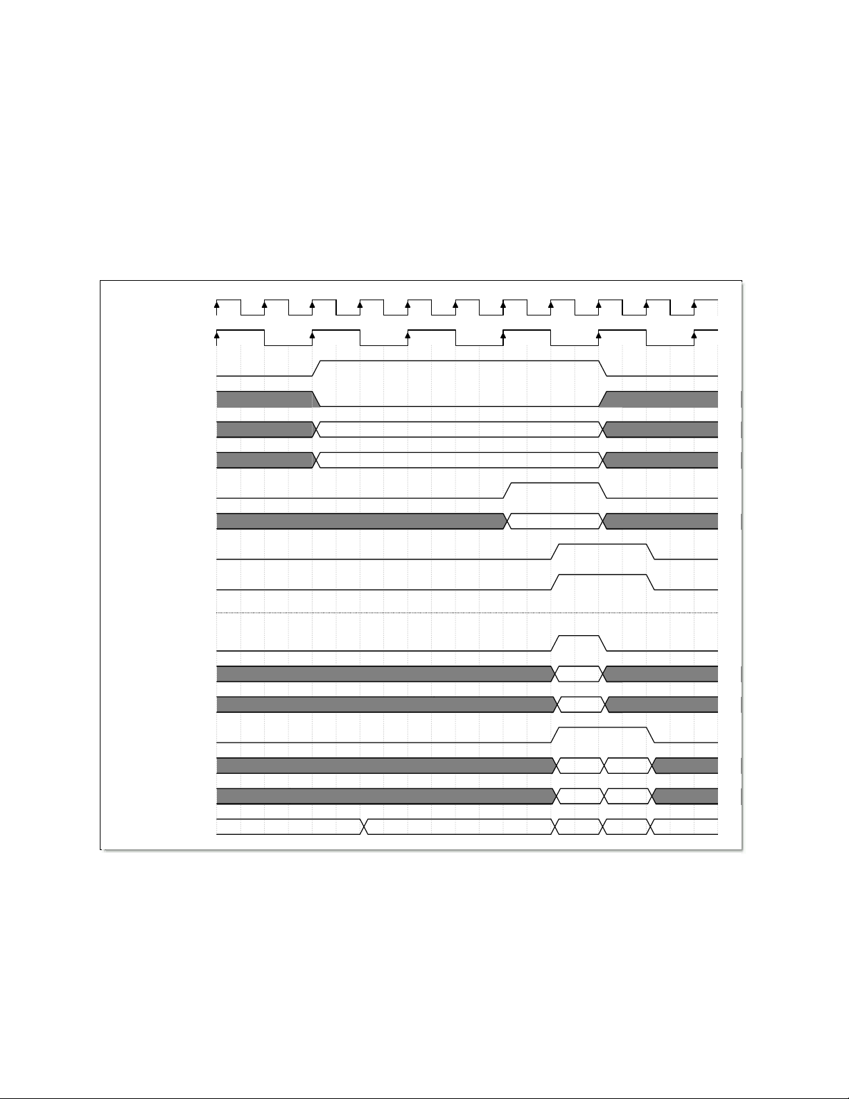
2.3.3 Burst Memory Write - Four 32-bit Words
DDR2_Clk
Bus2IP_Clk
Bus2IP_CS
Bus2IP_Burst
Bus2IP_RNW
Bus2IP_Addr
Bus2IP_BE
Bus2IP_WrReq
Bus2IP_Data
IP2Bus_A ddrAck
IP2Bus_W rAck
App_AF_WREn
App_AF_Cmd
App_AF_Addr
App_WDF_WREn
App_WDF_Data
App_WDF_Mask_Data
State
1 2 3 4 5 6 7 8 9 10 11 12 13 14 15 16 17
Address
Byte Enabl es (All 1's for a burst)
Word 1
Idle Wait_WrReq
Address+0x4 Address+0x8 Address+0xC
Word 2 Word 3 Word 4
Wri te
Address
Word 12 Word 34
0x0
Wr_Bur st1 Wr _Burst 2
Wr_B urs tD
IdleSave_W1 Save_W2 Save_W3
TimeGen
12/03/2010 07:35 AM 9
Copyright © 2009-2010 by CML
Page 10

Opus Card – DDR-2 Interface
Reference Manual
2.3.4 Burst Memory Write - Eight 32-bit Words
DDR2_Clk
Bus2IP_Clk
Bus2IP_CS
Bus2IP_Burst
Bus2IP_RNW
Bus2IP_Addr
Bus2IP_BE
Bus2IP_WrReq
Bus2IP_Data
IP2Bus_A ddrAck
IP2Bus_W rAck
App_AF_WREn
App_AF_Cmd
App_AF_Addr
App_WDF_WREn
App_WDF_Data
App_WDF_Mask_Data
State
1 2 3 4 5 6 7 8 9 10 11 12 13 14 15 16 17 18 19 20 21 22 23 24 25
Addr
Idle Wait_WrReq
Addr+0x4 Addr+0x8 Addr+0xC
Byte Enable s (All 1's for a burst)
Word 2 Wo rd 3 Word 4
Word 1
Save _W1
Save_W2 Save_W3
Wri te
Add r
Wd 12 Wd 3 4
0x0
Wr_Brst1 W r_Brst2
Addr+0x1CAddr+0x18Ad dr+0x14Addr+0x10
Word 5 Wo rd 6 Word 7 Word 8
Writ e
Addr+4
Wd 56 Wd78
0x0
Wr_BrstD Save _W1 Wr_BrstD
Save_W2 Save_W3
Wr_Brst1 Wr_Brst2
Idle
TimeGen
12/03/2010 07:35 AM 10
Copyright © 2009-2010 by CML
Page 11

Opus Card – DDR-2 Interface
Reference Manual
2.3.5 Burst Memory Write – Two 64-bit Words
DDR2_Clk
Bus2IP_Clk
Bus2IP_CS
Bus2IP_Burst
Bus2IP_RNW
1 2 3 4 5 6 7 8 9 10 11 12 13
Bus2IP_Addr
Bus2IP_BE
Bus2IP_WrReq
Bus2IP_Data
IP2Bus_AddrA ck
IP2Bus_W rA ck
App_AF_WREn
App_AF_Cmd
App_AF_Addr
App_WDF_WREn
App_WDF_Data
App_WDF_Mask_Data
State
Address
Byte Enables (All 1's for a burst)
Idle Wait_WrReq
Word 1
Save_W1
Address+0x8
Word 2
Wri te
Address
Word 1 Word 2
0x0
Wr_Bur st2
Wr_Bur st 1
Wr_Bur stD
Idle
TimeGen
12/03/2010 07:35 AM 11
Copyright © 2009-2010 by CML
Page 12

Opus Card – DDR-2 Interface
Reference Manual
2.3.6 Burst Memory Write - Four 64-bit Words
DDR2_Clk
Bus2IP_Clk
Bus2IP_CS
Bus2IP_Burst
Bus2IP_RNW
Bus2IP_Addr
Bus2IP_BE
Bus2IP_WrReq
Bus2IP_Data
IP2Bus_A ddrAck
IP2Bus_W rAck
App_AF_WREn
App_AF_Cmd
App_AF_Addr
App_WDF_WREn
App_WDF_Data
App_WDF_Mask_Data
State
1 2 3 4 5 6 7 8 9 10 11 12 13 14 15 16
Address
Byte Enable s (All 1's for a burst)
Word 1
Idle Wait_WrReq
Address+0x8 Address+0x10 Address+0x18
Word 2 Word 3 Word 4
Wri te
Addr es s
Word 1 Wo rd 2
0x0
Wr_Br st1 Wr_B rst2
Wr_B rs tD Wr_B rs tD
Save_W1
Wri te
Addr es s+4
Word 3 Wo rd 4
Wr_Br st1
0x0
Wr_B rs t2
IdleSave_W1
TimeGen
12/03/2010 07:35 AM 12
Copyright © 2009-2010 by CML
Page 13

Opus Card – DDR-2 Interface
Reference Manual
3. State Machines for Reading Data from Memory
This chapter covers the state machines that controls the reading of data requested via the PLB
bus from the DDR-2 Memory Controller. The read state machines support both non-burst reads
and burst reads. Burst reads are limited to a multiple of four 32-bit words or a multiple of two
64-bit words depending on the width of the PLB data bus and should be limited to a maximum
length of eight quad-words (128 bytes). Each burst is assumed to have consecutive addresses
starting with an address masked by 0xFFFFFFF0.
There are two state machines used for reading data from memory. The first is the read state
machine and the second is the read FIFO state machine. The first state machine controls the
reading of data from the DDR-2 memory controller to the read FIFO. To parallelize the reading
and writing to the read FIFO, the FIFO state machine was implemented to transfer data in the
FIFO to the PLB slave controller.
3.1 Signal Definitions
The table below provides details on the signals used for reading data from memory.
Name I/O Description
Bus2IP_Clk I The clock for the PLB bus (currently 100 MHz)
DDR2_Clk I The clock for the DDR-2 memory (currently 200 MHz)
Bus2IP_Reset I Reset signal for the block
App_AF_AFull I Indicates the DDR-2 address buffer is full – not currently used
Bus2IP_Addr I Address of DDR-2 memory to read from
Bus2IP_CS I Indicates the DDR-2 memory is being accessed
Bus2IP_Burst I Indicates a burst read or write is occurring
Bus2IP_BurstLength I Indicates the length of the burst in bytes
Bus2IP_RNW I Indicates a read access when high
Bus2IP_RdReq I Indicates a read request
Rd_Data_Valid I Indicates the data is valid from the DDR-2 memory controller
Rd_Data_FIFO_Out I Data read from the DDR-2 memory
IP2Bus_Data O Data read from the DDR-2 memory that is returned to the PLB
slave when IP2Bus_RdAck is asserted
Rd_Burst_Cnt O Current burst count value that is added to App_AF_AAFull
during a burst read
Rd_Send_Ack O Acknowledges the read from the PLB slave and signals that the
IP2Bus_Data is valid during the next clock cycle
Rd_Send_Cmd O Indicates the read command and address should be sent to the
DDR-2 memory controller on the next clock cycle
12/03/2010 07:35 AM 13
Copyright © 2009-2010 by CML
Page 14

Opus Card – DDR-2 Interface
Reference Manual
3.2 Read State Machine
The read state machine currently has eight states to support the reading of data from memory via
the DDR-2 memory controller. Transitions from one state to the next occur on the rising edge of
DDR2_Clk and the state machine is synchronously reset to Idle when Bus2IP_Reset is ‘1’. Each
state is described below:
State Description
Idle Waiting for a read request from the PLB slave. A read is detected when
Bus2IP_CS is ‘1’, Bus2IP_RdReq is ‘1’, and App_AF_AFull is ‘0’. The state
machine then transitions to Wait_RdValid on the next clock during a non-burst
read. During a burst read, the state machine transitions to Wait_RdValid one
clock after the last address of the burst is queued to the DDR-2 controller.
Wait_RdValid Waiting for Rd_Data_Valid to transition to ‘1’ to indicate the data has been read
from memory and is present on Rd_Data_FIFO_Out. The state machine
transitions to Rd_Align when Bus2IP_Clk is ‘1’ on a non-burst read.
Otherwise, the state machine transitions toRd_Ack1 on a non-burst read.
For a burst-read, the state machine transitions to Queue_D1 when
Rd_Data_Valid is ‘1’.
Rd_Align Nothing occurs during this state but it does cause the state machine to align with
Bus2IP_Clk. The state machine transitions to Rd_Ack1 on the next clock.
Rd_Ack1 State that acknowledges the read from the PLB slave and places the data for the
requested memory address on IP2Bus_Data. The state machine transitions to
Rd_Ack2 on the next clock.
Rd_Ack2 State that acknowledges the read from the PLB slave and places the data for the
requested memory address on IP2Bus_Data. The state machine transitions to
Idle on the next clock.
Queue_D1 State that indicates the first word has been saved to the FIFO during a burst
read. The state machine transitions to Queue_D2 when Rd_Data_Valid is ‘1’.
Otherwise, the state machine remains in this state.
Queue_D2 State that indicates the second word has been saved to the FIFO during a burst
read. The state machine transitions to Queue_D1 if the reading of the data is
not complete when Rd_Valid is ‘1’. When done reading data from the DDR-2
controller, the state machine transitions to the FIFO_Read state.
FIFO_Read This state is used to wait for the FIFO state machine to complete the transfer of
data read from the DDR-2 memory controller to the PLB slave. The state
machine transitions to the Idle state when the burst transfer to the PLB slave is
completing the last word in the transfer.
12/03/2010 07:35 AM 14
Copyright © 2009-2010 by CML
Page 15

Opus Card – DDR-2 Interface
Reference Manual
3.2 Read FIFO State Machine
The Read FIFO state machine currently has four states to support the reading of data from the
read FIFO to the PLB slave. Transitions from one state to the next occur on the rising edge of
DDR2_Clk and the state machine is synchronously reset to Idle when Bus2IP_Reset is ‘1’. Each
state is described below:
State Description
Idle Waiting for the read FIFO to contain data during a burst read. The state
machine transitions to the FIFO_Rd state once data is detected in the read FIFO.
FIFO_Rd For a 64-bit PLB slave, the state machine transitions to the Lo_Bits state when
Bus2IP_Clk is currently ‘1’. For a 32-bit PLB slave, the state machine
transitions to the Hi-Bits state when Bus2IP_Clk is currently ‘1’.
Hi_Bits This state is only used for a 32-bit PLB slave and will cause the high order bits
of the read FIFO to be placed on the IP2Bus_Data bus. The state machine
transitions to the Lo_Bits state when Bus2IP_Clk is currently ‘1’.
Lo_Bits This state will output the read FIFO data to the IP2Bus_Data bus. For a 64-bit
PLB slave, the read FIFO data is placed on the IP2Bus_Data bus. For a 32-bit
PLB slave, the low order bits of the read FIFO are placed on the IP2Bus_Data
bus. The state machine transitions to FIFO_Rd when there is data left to
transfer. Otherwise the state machine will transition to Idle when Bus2IP_Clk is
currently ‘1’.
12/03/2010 07:35 AM 15
Copyright © 2009-2010 by CML
Page 16

Opus Card – DDR-2 Interface
Reference Manual
3.3 Waveforms
3.3.1 Non-burst, 32-bit Memory Read Clock-Aligned
The timing diagram below is for a non-burst, 32-bit memory read where Rd_Data_Valid aligns
with the rising edge of Bus2IP_Clk.
DDR2_Clk
Bus2IP_Clk
Bus2IP_CS
Bus2IP_RNW
1 2 3 4 5 6 7 8 9 10 11 12
Bus2IP_Addr
Bus2IP_RdReq
IP2B us_Data
Rd_Send_Cmd
Rd_Send_Ack
Rd_Data_Valid
Rd_Data_FIFO_Out
State
IP2B us_AddrAc k
IP2B us_RdAc k
App_AF_WREn
App_AF_Cmd
App_AF_Addr
Idle Wait_RdVal id Rd_Ali gn IdleWai t_RdV ali d Rd_ Ack1 Rd_A ck2
Signals below are from write_ctrl
Rea d
Address
Address
Word 1 Wo rd2
32-bit Data
TimeGen
12/03/2010 07:35 AM 16
Copyright © 2009-2010 by CML
Page 17

Opus Card – DDR-2 Interface
Reference Manual
3.3.2 Non-burst, 32-bit Memory Read not Clock-Aligned
The timing diagram below is for a non-burst, 32-bit memory read where Rd_Data_Valid does
not align with the rising edge of Bus2IP_Clk.
DDR2_Clk
Bus2IP_Clk
Bus2IP_CS
Bus2IP_RNW
1 2 3 4 5 6 7 8 9 10 11 12
Bus2IP_Addr
Bus2IP_RdReq
IP2B us_Data
Rd_Send_Cmd
Rd_Send_Ack
Rd_Data_Valid
Rd_Data_FIFO_Out
State
IP2B us_AddrAc k
IP2B us_RdAc k
App_AF_WREn
App_AF_Cmd
App_AF_Addr
Idle Wait_RdVal id IdleWai t_ RdV al id Rd _Ac k1 Rd_ Ack2
Signals below are from write_ctrl
Rea d
Address
Address
Word 1 Word2
32-bit Data
TimeGen
12/03/2010 07:35 AM 17
Copyright © 2009-2010 by CML
Page 18

Opus Card – DDR-2 Interface
Reference Manual
3.3.3 Non-burst, 64-bit Memory Read
The timing diagram below is for a non-burst, 64-bit memory read where Rd_Data_Valid aligns
with the rising edge of Bus2IP_Clk. The non-aligned version of the read is similar except the
Rd_Align state is skipped.
DDR2_Clk
Bus2IP_Clk
Bus2IP_CS
Bus2IP_RNW
1 2 3 4 5 6 7 8 9 10 11 12
Bus2IP_Addr
Bus2IP_RdReq
IP2B us_Data
Rd_Send_Cmd
Rd_Send_Ack
Rd_Data_Valid
Rd_Data_FIFO_Out
State
IP2B us_AddrAc k
IP2B us_RdAc k
App_AF_WREn
App_AF_Cmd
App_AF_Addr
Idle Wait_RdVal id Rd_Ali gn IdleWai t_RdV ali d Rd_ Ack1 Rd_A ck2
Signals below are from write_ctrl
Rea d
Address
Address
Word 1 Wo rd2
64-bit Data
TimeGen
12/03/2010 07:35 AM 18
Copyright © 2009-2010 by CML
Page 19

Opus Card – DDR-2 Interface
Reference Manual
3.3.4 Burst Memory Read - Four 32-bit Words
The timing diagram below is for a four 32-bit word burst read. Data is buffered to a FIFO as it is
read from the DDR-2 controller. The data is then read from the FIFO as it is transferred to the
PLB slave.
DDR2_Clk
Bus2IP_Clk
Bus2IP_CS
Bus2IP_Burst
Bus2IP_BurstLength
Bus2IP_RNW
Bus2IP_Addr
Bus2IP_RdReq
IP2Bus_Data
Rd_Send_Cmd
burst_ack
Rd_Send_A ck
Rd_Data_Valid
Rd_Data_FIFO_Out
Rd_Burst _Cnt
rdfifo_empty
rdfifo_rden
State
FIFO_State
IP2Bus_A ddrAck
IP2Bus_RdAc k
App_AF_WREn
App_AF_Cmd
App_AF_Addr
1 2 3 4 5 6 7 8 9 10 11 12 13 14 15 16 17 18 19
0x10
Address
Word 12 Wor d 34
0x0 0x1 0x0
Queu e_ D1
Idle
Idle Idle
Queu e_D 2 FIFO_R ead
FIFO_Rd FIFO_RdHi_Bits Lo_Bits Lo_BitsHi_Bits
Address + 0x04 Address + 0x08 Address + 0x0C
Word 1
Wor d2 Word 3 Word4
IdleWai t_Rd Val id
Signals below are from write_ctrl
Read
Address
TimeGen
12/03/2010 07:35 AM 19
Copyright © 2009-2010 by CML
Page 20

Opus Card – DDR-2 Interface
Reference Manual
3.3.5 Burst Memory Read - Eight 32-bit Words
The timing diagram below is for an eight 32-bit word burst read. Data is buffered to a FIFO as it
is read from the DDR-2 controller. The data is then read from the FIFO as it is transferred to the
PLB slave.
DDR2_Clk
Bus2IP_Clk
Bus2IP_CS
Bus2IP_Burst
Bus2IP_BurstLength
Bus2IP_RNW
Bus2IP_Addr
Bus2IP_RdReq
IP2Bus_Data
Rd_Send_Cmd
burst_ack
Rd_Send_Ack
Rd_Data_V alid
Rd_Data_F IFO_Out
Rd_Burs t_Cnt
rdfifo_empty
rdfifo_rden
State
FIFO_State
IP2Bus_AddrA ck
IP2Bus_RdAc k
App_AF_WREn
App_AF_Cmd
App_AF_Addr
1 2 3 4 5 6 7 8 9 10 11 12 13 14 15 16 17 18 19 20 21 22 23 24 25 26 27
0x20
Address
Word 12 Wo rd 3 4
0x0 0x2 0x0
0x1 0x2
Idle
Idle Idle
Q_D1
F_Rd F_RdHi_Bits Lo_Bits Lo_BitsHi_Bits
Add ress + 0x0 4
Word 1
Word 5 6 Word 78
0x1
Q_D1 Q_D2
Queue_ D 2 FIFO_Read
Add res s + 0x0 8 Addr ess + 0 x0 C
Wor d2 Word3 Wo rd4
Add ress + 0x1 0 Addre ss + 0 x1 4 Add ress + 0x1 8 Add re ss + 0x1 C
Word 5 Word6 Wo rd7 Wo rd8
IdleWai t_ RdV al i d
F_Rd F_RdHi_Bits Hi_BitsLo_Bits Lo_Bits
Signals below are from write_ctrl
Rea d
Rea d
Add r+4
Add r
TimeGen
12/03/2010 07:35 AM 20
Copyright © 2009-2010 by CML
Page 21

Opus Card – DDR-2 Interface
Reference Manual
3.3.6 Burst Memory Read - Two 64-bit Words
The timing diagram below is for a two 64-bit word burst read. Data is buffered to a FIFO as it is
read from the DDR-2 controller. The data is then read from the FIFO as it is transferred to the
PLB slave.
DDR2_Clk
Bus2IP_Clk
Bus2IP_CS
Bus2IP_Burst
Bus2IP_BurstLength
Bus2IP_RNW
Bus2IP_Addr
Bus2IP_RdReq
IP2Bus_ Data
Rd_Send_Cm d
burst_ack
Rd_Send_A ck
Rd_Dat a_V ali d
Rd_Dat a_FIFO_Out
Rd_Burst_Cnt
rdfifo_empty
rdfifo_rden
State
FIFO_State
1 2 3 4 5 6 7 8 9 10 11 12 13 14 15
0x10
Word 1
Address + 0x08
Wor d2
IdleWai t_ RdV al id
Address
Word 1 Wo rd 2
0x0 0x1 0x0
Queue _D1
Idle
Idle Idle
Queu e_D2 FIFO_Re ad
FIFO_Rd FIFO_RdLo_Bi ts Lo_Bi ts
IP2Bus_ AddrA ck
IP2Bus_ RdAck
App_AF_WREn
App_AF_Cmd
App_AF_Addr
Signals below are from write_ctrl
Rea d
Address
TimeGen
12/03/2010 07:35 AM 21
Copyright © 2009-2010 by CML
Page 22

Opus Card – DDR-2 Interface
Reference Manual
3.3.7 Burst Memory Read - Four 64-bit Words
The timing diagram below is for a four 64-bit word burst read. Data is buffered to a FIFO as it is
read from the DDR-2 controller. The data is then read from the FIFO as it is transferred to the
PLB slave.
DDR2_Clk
Bus2IP_Clk
Bus2IP_CS
Bus2IP_Burst
Bus2IP_BurstLength
Bus2IP_RNW
Bus2IP_Addr
Bus2IP_RdReq
IP2Bus_Data
Rd_Send_Cmd
burst_ack
Rd_Send_A ck
Rd_Data_Valid
Rd_Data_FIFO_Out
Rd_Burst_Cnt
rdfifo_empty
rdfifo_rden
State
FIFO_State
IP2Bus_A ddrAck
IP2Bus_RdAc k
App_AF_WREn
App_AF_Cmd
App_AF_Addr
1 2 3 4 5 6 7 8 9 10 11 12 13 14 15 16 17 18 19
0x20
Address
Word 12 Word 34
0x1 0x2
0x0 0x2 0x0
Idle
Queu e_ D1
Idle Idle
Queue_ D 2 FIFO_Read
FIFO_Rd Lo_Bits Lo_Bits
Address + 0x08 Address + 0x10 Address + 0x18
Wor d1
Word 56 Word 78
0x1
Queue_ D 1 Queue_ D 2
FIFO_Rd FIFO_Rd FIFO_Rd
Word 2 Word 3 Wo rd4
Lo_Bits Lo_Bits
IdleWai t_Rd Val id
Signals below are from write_ctrl
Rea d
Read
Addr+4
Add r
TimeGen
12/03/2010 07:35 AM 22
Copyright © 2009-2010 by CML
 Loading...