

Page 1
DDiiggiilleenntt DD22--SSBB SSyysstteemm BBooaarrdd
RReeffeerreennccee MMaannuuaal
June 4, 2004 246 East Main | Pullman, WA 99163
l
www.digilentinc.com
(509) 334 6306 Voice and Fax
Overview
The Digilent D2-SB circuit board provides a
complete circuit development platform
centered on a Xilinx Spartan 2E FPGA. D2-SB
features include:
• A Xilinx XC2S200E-200 FPGA with 200K
gates and 350MHz operation;
• 143 user I/Os routed to six standard 40pin expansion connectors;
• A socket for a JTAG-programmable
18V02 configuration Flash ROM;
• Dual on-board 1.5A power regulators
(1.8V and 3.3V);
• An SMD 50MHz oscillator, and a socket
for a second oscillator;
• A JTAG programming port;
• A status LED and pushbutton for basic
I/O.
The D2-SB has been designed to work
seamlessly with all versions of the Xilinx ISE
CAD tools, including the free WebPack tools
available from the Xilinx website. A growing
collection of low-cost expansion boards can be
used with the D2-SB to add analog and digital
I/O capabilities, as well as various data ports
like Ethernet and USB. The D2-SB board ships
with a power supply and programming cable,
so designs can be implemented immediately
without the need for any additional hardware.
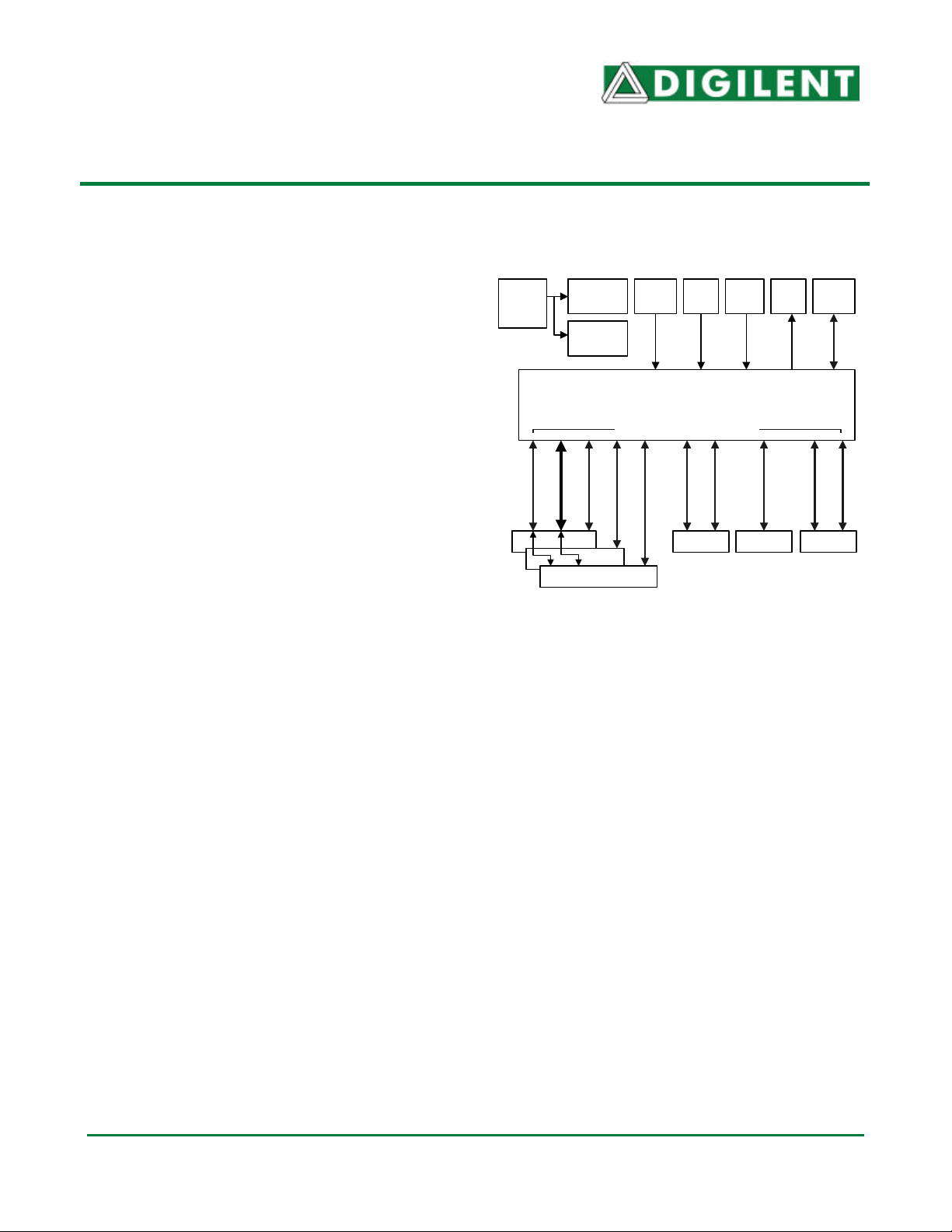
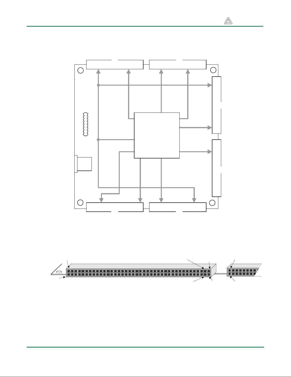
Functional Description
The Digilab D2-SB provides a minimal system
that can be used to rapidly implement FPGAbased circuits, or to gain exposure to Xilinx
CAD tools and Spartan 2E devices. The D2-SB
provides only the essential supporting devices
for the Spartan 2E FPGA, including clock
sources and power supplies. All available I/O
signals are routed to standard expansion
Power
jack
5-9VDC
1.8VDC
regulator
3.3VDC
regulator
Clock
(50MHz)
ND
2
Clock
Push
button
LED
Config
ROM
JTAG
Xilinx Spartan2E XC2S200E-PQ208
Expansion Connectors
JTAG
MA1 bus
System Bus
A1
B1
MB1 bus
MC1 bus
C1
PA bus
MA2 bus
A2 B2 C2
PB bus
MC2 bus
Figure 1. D2-SB Circuit Board Block Diagram
connectors that mate with 40-pin, 100 mil
spaced DIP headers available from any
catalog distributor. A pushbutton and LED are
also included for basic I/O. (See Figure 1)
The D2-SB board has been designed to serve
primarily as a host for peripheral boards. Each
of the six expansion connectors provides the
unregulated supply voltage (VU), 3.3V, GND,
and 32 FPGA I/O signals. Because there are
more connector pins than FPGA pins, the A1,
B1 and C1 connectors share an 18-pin “system
bus”, and not all pins on the B expansion
connectors are used. JTAG signals are also
routed to the A1, B1, and C1 expansion
connectors. This allows peripheral boards to
drive the scan chain, or to be configured along
with the Spartan 2E FPGA.
Application-specific peripheral boards can be
created to mate with the D2-SB, or readymade peripheral boards that offer many
PC bus
Copyright Digilent, Inc. All rights reserved 7 pages Doc: 502-023
Page 2
D2-SB Reference Manual Digilent, Inc.
standard functions can be obtained from
Digilent (see www.digilentinc.com).
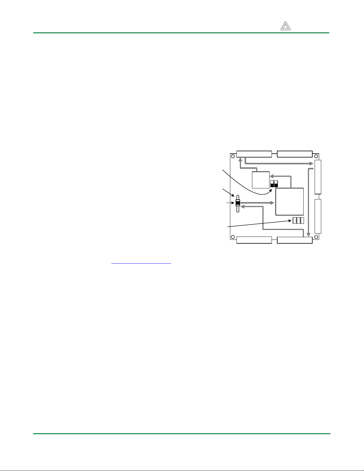
JTAG Ports and Device Configuration
The Spartan 2E FPGA , the 18V00 ROM on
the D2-SB, and any programmable devices on
peripheral boards attached to the D2-SB can
be programmed via the JTAG port. The JTAG
scan chain is routed to the FPGA and ROM on
the D2-SB and then around the board to four
connection ports as shown in Figure 2. The
primary configuration port (Port 1) uses a
standard 6-pin JTAG header (J7) that can
accommodate Digilent’s JTAG3 cable (or
cables from Xilinx or other vendors). The other
three JTAG programming ports are available
on the A1, B1, and C1 expansion connectors,
and these ports are bi-directional. If no
peripheral board is present, a buffer on the D2SB removes the expansion connector from the
JTAG chain. If a peripheral board with a JTAG
device is attached, the scan chain is driven out
the expansion connector so that any JTAGprogrammable parts can be configured. If a
Digilent port module is connected to one of the
three JTAG-enabled expansion connectors,
then the port module can drive the JTAG chain
to program all devices in the scan chain (port
modules include Ethernet, USB, EPP parallel,
and serial modules -- see www.digilentinc.com
for more information).
The scan chain can be driven from the primary
port by powering on the D2-SB, connecting it
to a PC with a JTAG programming cable, and
running the “auto-detect” feature of the
configuration software. The configuration
software allows devices in the scan chain to be
selectively programmed with any available
configuration file. If no programming ROM is
loaded in the IC5 socket (or if ROM is present
but is not to be included in the scan chain),
jumper-shunts must be loaded at JP1 and JP2
in the “Bypass ROM” location to route the
JTAG chain around the ROM socket. If an
18V02 (or larger) ROM is loaded in the IC5
socket, it can be included in the scan chain by
loading the JP1 and JP2 jumper-shunts in the
“Include ROM” positions.
If a programming ROM is present in the IC5
socket, the FPGA will automatically access the
ROM for configuration data if jumper shunts
are loaded in all three positions of J8 (M2, M1,
and M0).
Port modules attached to ports A1, B1, or C1
can drive the scan chain if a jumper-shunt is
installed on the primary JTAG header across
the TDI and TDO pins. In their default state,
Digilent port modules will appear as a JTAG
cable to the configuration software. Port
modules can disable their JTAG drivers; if
more than one JTAG driver is enabled on the
scan chain, programming may fail.
Port 2
ROM bypass
jumpers
JTAG
connector
Cable bypass
jumper
Programming
mode select
jumpers
A1
18V
ROM
Port 1
C2
A2
Spartan 2E
PQ 208
C1
Port 4
B1 B2
Port 3
Figure 2. JTAG Signal Routing on D2-SB
Power Supplies
The D2-SB board uses two LM317 voltage
regulators to produce a 1.8VDC supply for the
Spartan 2E core, and 3.3VDC supply for the
I/O ring. Both regulators have good bypass
capacitance, allowing them to supply up to
1.5A of current with less than 50mV of noise
(typical). Power can be supplied from a lowcost wall transformer supply. The external
supply must use a 2.1mm center-positive
connector, and it must produce between 6VDC
and 12VDC of unregulated voltage.
The D2-SB uses a four layer PCB, with the
inner layers dedicated to VCC and GND
planes. Most of the VCC plane is at 3.3V, with
an island under the FPGA at 1.8V. The FPGA
and the other ICs on the board all have
0.047uF bypass capacitors placed as close as
possible to each VCC pin.
www.digilentinc.com © Digilent, Inc. Page 2
Page 3
D2-SB Reference Manual Digilent, Inc.
Total board current is dependant on FPGA
configuration, clock frequency, and external
connections. In test circuits with roughly 50K
gates routed, a 50MHz clock source, and a
single expansion board attached (the DIO5
board), approximately 200mA +/- 30% of
supply current is drawn from the 1.8V supply,
and approximately 200mA +/- 50% is drawn
from the 3.3V supply. These currents are
strongly dependent on FPGA and peripheral
board configurations.
All FPGA I/O signals use the VCCO voltage
derived from the 3.3V supply. If other VCCO
voltages are required, the regulator output can
be modified by changing R12 according to:
VCCO = 1.25(1 + R12/R11).
Refer to the LM317 data sheet and D2-SB
schematic for further information.
Oscillators
The D2-SB provides a 50MHz SMD primary
oscillator and a socket for a second oscillator.
The primary oscillator is connected to the
GLK2 input of the Spartan 2E (pin 182), and
the secondary oscillator is connected to
GCLK3 (pin 185). Both clock inputs can drive
the DLL on the Spartan 2E, allowing for
internal frequencies up to four times higher
than the external clock signals. Any 3.3V
oscillator in a half-size DIP package can be
loaded into the secondary oscillator socket.
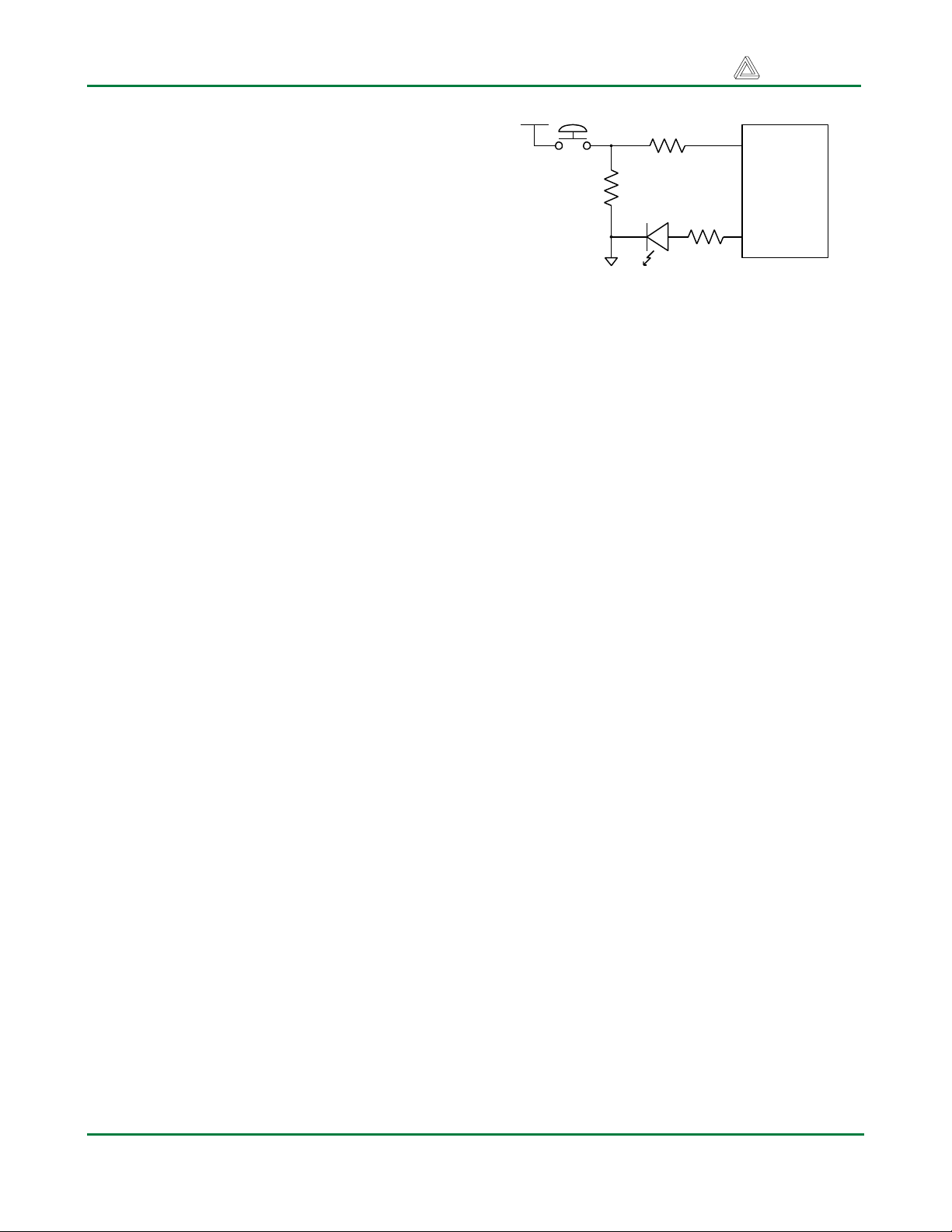
Pushbutton and LED
A single pushbutton and LED are provided on
the board allowing basic status and control
functions to be implemented without a
peripheral board. As examples, the LED can
be illuminated from a signal in the FPGA to
verify that configuration has been successful,
and the pushbutton can be used to provide a
basic reset function independent of other
inputs. The circuits are shown in Figure 2.
Vdd
Push
button
4.7K
4.7K
80 Ohm
Pin 187
Xilinx
Spartan 2E
PQ208
Pin 154
Figure 2. Pushbutton and LED Circuit
Expansion Connectors
The six expansion connectors labeled A1-A2,
B1-B2, and C1-C2 use 2x20 right-angle
headers with100 mil spacing. All six
connectors have GND on pin 1, VU on pin 2,
and 3.3V on pin 3. Pins 4-35 route to FPGA I/O
signals, and pins 36-40 are reserved for JTAG
and/or clock signals. (See Figure 4.)
The expansion headers provide 192 signal
connections, but the Spartan 2E-PQ208 has
only 143 available I/O signals. Thus, some
FPGA signals are routed to more than one
connector. In particular, the lower 18 pins (pins
4-21) of the A1, B1, and C1 connectors are all
connected to the same 18 FPGA pins, and
they are designated as the “system bus” (a
unique chip select signal is routed to each
connector). Other than these 18 shared
signals, all remaining FPGA signals are routed
to individual expansion connector positions.
The lower 18 pins of the A2, B2, and C2
connectors are designated as “peripheral
busses”, and each of these busses (named
PA, PB, and PC) use 18 unique signals.
The 14 upper pins of each expansion
connector (pins 22-35) have been designated
as “module busses”. The A1, A2, C1, and C2
connectors each have fully populated module
busses (named MA1, MA2, MC1, and MC2).
Insufficient FPGA pins were available to route
full module buses to the B connectors; only the
8 data pins of MB1 are routed, and no pins are
routed to the upper B2 expansion connector
(i.e., MB2 is a “no connect”).
www.digilentinc.com © Digilent, Inc. Page 3
Page 4
D2-SB Reference Manual Digilent, Inc.
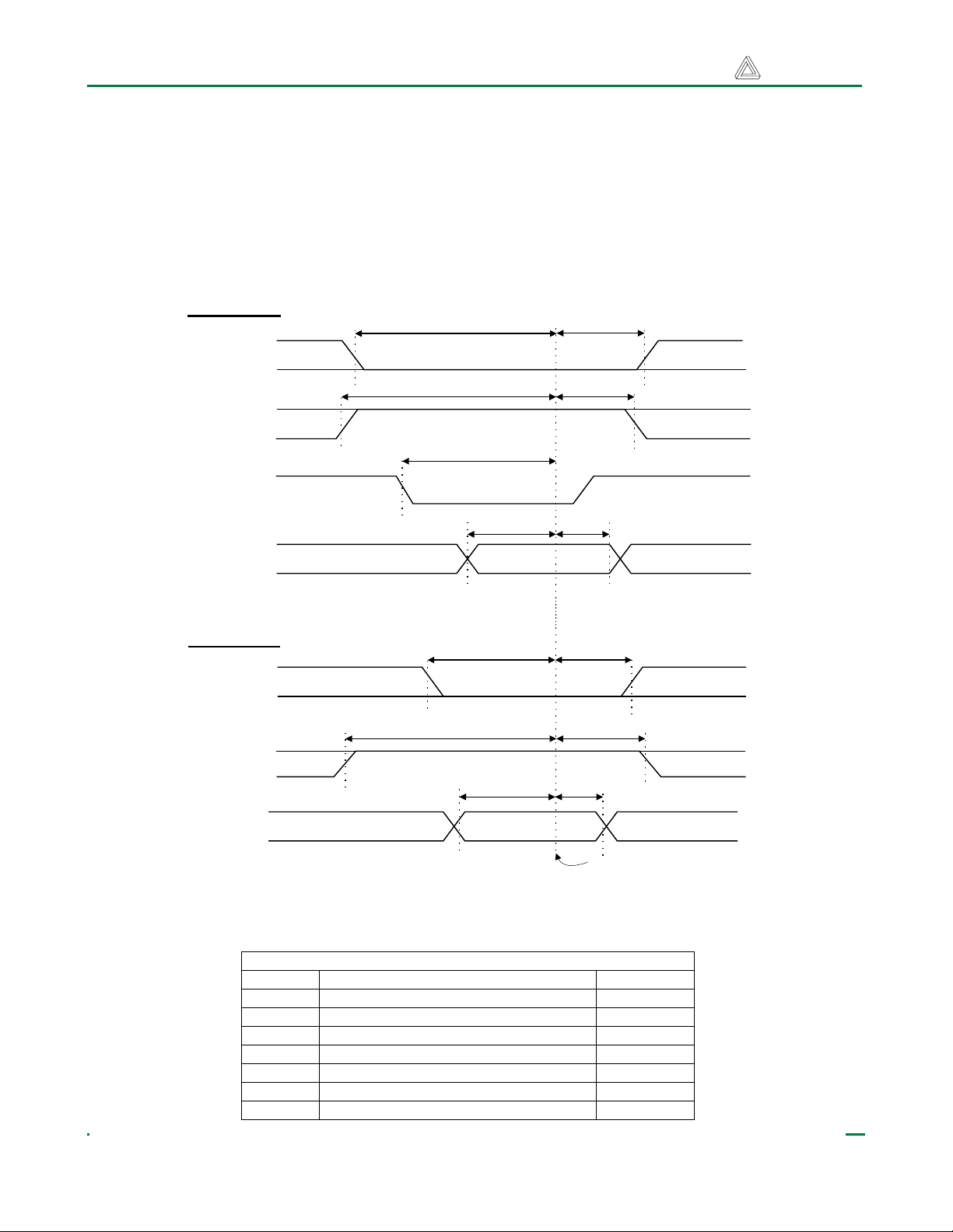
System Bus
The “system bus” is a protocol used by certain
expansion boards that mimics a simple 8-bit
microprocessor bus. It uses eight data lines,
six address lines, a write-enable (WE) strobe
that can be used by the peripheral to latch
written data, an output-enable (OE) strobe that
Write Cycle
CS
tdoe
OE
WE
DB0-DB7
ten
can be used by the peripheral to enable read
data, a chip select, and a clock to enable
synchronous transfers. The diagrams, (Figure
3), below show signal timings assumed by
Digilent to create peripheral devices. However,
any bus and timing models can be used by
modifying circuits in the FPGA and attached
peripheral devices.
th
teoe
tw
tsu
th
Read Cycle
OE
WE
DB0-DB7
Symbol Parameter Time (typ)
tdoe Time to disable after OE de-asserted 10ns
teoe Time to enable after OE asserted 15ns
teoe
twd
tsu
tdoe
th
th
Read data latch time
Figure 3. System Bus Timing
Table 1. System Bus Timing
ten Time to enable after CS asserted 10ns
th Hold time 1ns
tw Write strobe time 10ns
tsu Data setup time 5ns
twd Write disable time 0ns
www.digilentinc.com © Digilent, Inc. Page 4
Page 5
D2-SB Reference Manual Digilent, Inc.
pins 4 -21
A1
pins 22 -35 pins 4 -21 pins 22 -35
A2
pins 4 -21
MA1 (14)
MA2(14)
B1
pins 22 -35 pins 4 -21 pins 22 -35
Sys Bus (18)
Spartan 2E
PQ 208
MB1(8)
PB(18)
B2
MC2(14)
PC(18)
MC1(14) PA(18)
pins 22 -35 pins 4 -21pins 22 -35
Figure 4. Expansion Connector Signal Routing
C2
pins 4 -21
C1
Pin 39
Pin 3: 3.3V
Pin 1: GND
Pin 39
Pin 40
Pin 4
Figure 5. Expansion Connector Pin Locations
Pin 2: VU
Pin 40
www.digilentinc.com © Digilent, Inc. Page 5
Page 6

D2-SB Reference Manual Digilent, Inc.
1
2
3
4
5
6
7
8
9
10
11
12
13
14
15
16
17
18
19
20
21
22
23
24
25
26
27
28
29
30
31
32
33
34
35
36
37
38
39
40
Table 2. D2-SB Expansion Connector Pinout
A1 A2 B1 B2 C1 C2
Pin #
Signal
GND GND GND GND GND GND
VU VU VU VU VU VU
VCC33 VCC33 VCC33 VCC33 VCC33 VCC33
ADR0 112 PAI01 162 ADR0 112 PBI01 71 ADR0 112 PCI01 23
DB0 111 PAI02 161 DB0 111 PBI02 70 DB0 111 PCI02 22
ADR1 110 PAI03 160 ADR1 110 PBI03 69 ADR1 110 PCI03 21
DB1 109 PAI04 152 DB1 109 PBI04 68 DB1 109 PCI04 20
ADR2 108 PAI05 151 ADR2 108 PBI05 64 ADR2 108 PCI05 18
DB2 102 PAI06 150 DB2 102 PBI06 63 DB2 102 PCI06 17
ADR3 101 PAI07 149 ADR3 101 PBI07 62 ADR3 101 PCI07 16
DB3 100 PAI08 148 DB3 100 PBI08 61 DB3 100 PCI08 15
ADR4 99 PAI09 147 ADR4 99 PBI09 60 ADR4 99 PCI09 11
DB4 98 PAI010 146 DB4 98 PBI010 59 DB4 98 PCI010 10
ADR5 97 PAI011 145 ADR5 97 PBI011 58 ADR5 97 PCI011 9
DB5 96 PAI012 141 DB5 96 PBI012 57 DB5 96 PCI012 8
WE 95 PAI013 140 WE 95 PBI013 56 WE 95 PCI013 7
DB6 94 PAI014 139 DB6 94 PBI014 55 DB6 94 PCI014 6
OE 93 PAI015 138 OE 93 PBI015 49 OE 93 PCI015 5
DB7 89 PAI016 136 DB7 89 PBI016 48 DB7 89 PCI016 4
CSA 181 PAI017 135 CSB 88 PBI017 47 CSC 45 PCI017 3
LSBCLK 87 PAI018 134 LSBCLK 87 PBI018 46 LSBCLK 87 PCI018 206
MA1DB0 180 MA2DB0 133 MB1DB0 86 MC1DB0 44 MC2DB0 205
MA1DB1 179 MA2DB1 132 MB1DB1 84 MC1DB1 43 MC2DB1 204
MA1DB2 178 MA2DB2 129 MB1DB2 83 MC1DB2 42 MC2DB2 203
MA1DB3 176 MA2DB3 127 MB1DB3 82 MC1DB3 41 MC2DB3 202
MA1DB4 175 MA2DB4 126 MB1DB4 81 MC1DB4 40 MC2DB4 201
MA1DB5 174 MA2DB5 125 MB1DB5 75 MC1DB5 36 MC2DB5 200
MA1DB6 173 MA2DB6 123 MB1DB6 74 MC1DB6 35 MC2DB6 199
MA1DB7 169 MA2DB7 122 MB1DB7 73 MC1DB7 34 MC2DB7 198
MA1ASTB 168 MA2ASTB 121 MC1ASTB 33 MC2ASTB 194
MA1DSTB 167 MA2DSTB 120 MC1DSTB 31 MC2DSTB 193
MA1WRT 166 MA2WRT 116 MC1WRT 30 MC2WRT 192
MA1WAIT 165 MA2WAIT 115 MC1WAIT 29 MC2WAIT 191
MA1RST 164 MA2RST 114 MC1RST 27 MC2RST 189
MA1INT 163 MA2INT 113 MC1INT 24 MC2INT 188
JTSELA JTSELB JTSELC
TMS TMS TMS
TCK TCK TCK
TDO GCLK0 80 TDO TDO GCLK1 77
TDI GND TDI TDI GND
FPGA
Pin
Signal
FPGA
Pin
Signal
FPGA
Pin
Signal
FPGA
Pin
Signal
FPGA
Pin
Signal
FPGA
Pin
www.digilentinc.com © Digilent, Inc. Page 6
Page 7

D2-SB Reference Manual Digilent, Inc.
Pin # Function Pin # Function Pin # Function Pin # Function
1 GND 53 VCCO 105 VCCO 157 TDO
2 TMS 54 M2 106 PROG 158 GND
3 PC-IO17 55 PB-IO14 107 INIT 159 TDI
4 PC-IO16 56 PB-IO13 108 ADR2 160 PA-IO3
5 PC-IO15 57 PB-IO12 109 DB1 161 PA-IO2
6 PC-IO14 58 PB-IO11 110 ADR1 162 PA-IO1
7 PC-IO13 59 PB-IO10 111 DB0 163 MA1-INT
8 PC-IO12 60 PB-IO9 112 ADR0 164 MA1-RST
9 PC-IO11 61 PB-IO8 113 MA2-INT 165 MA1-WAIT
10 PC-IO10 62 PB-IO7 114 MA2-RST 166 MA1-WRT
11 PC-IO9 63 PB-IO6 115 MA2-WAIT 167 MA1-DSTB
12 GND 64 PB-IO5 116 MA2-WRT 168 MA1-ASTB
13 VCCO 65 GND 117 GND 169 MA1-DB7
14 VCCINTT 66 VCCO 118 VCCO 170 GND
15 PC-IO8 67 VCCINT 119 VCCINT 171 VCCO
16 PC-IO7 68 PB-IO4 120 MA2-DSTB 172 VCCINT
17 PC-IO6 69 PB-IO3 121 MA2-ASTB 173 MA1-DB6
18 PC-IO5 70 PB-IO2 122 MA2-DB7 174 MA1-DB5
19 GND 71 PB-IO1 123 MA2-DB6 175 MA1-DB4
20 PC-IO4 72 GND 124 GND 176 MA1-DB3
21 PC-IO3 73 MB1-DB7 125 MA2-DB5 177 GND
22 PC-IO2 74 MB1-DB6 126 MA2-DB4 178 MA1-DB2
23 PC-IO1 75 MB1-DB5 127 MA2-DB3 179 MA1-DB1
24 MC1-INT 76 VCCINT 128 VCCINT 180 MA1-DB0
25 GND 77 GCLK1 129 MA2-DB2 181 CSA
26 VCCO 78 VCCO 130 VCCO 182 GCLK2
27 MC1-RST 79 GND 131 GND 183 GND
28 VCCINT 80 GCLK0 132 MA2-DB1 184 VCCO
29 MC1-WAIT 81 MB1-DB4 133 MA2-DB2 185 GCLK3
30 MC1-WRT 82 MB1-DB3 134 PA-IO18 186 VCCINT
31 MC1-DSTB 83 MB1-DB2 135 PA-IO17 187 BTN
32 GND 84 MB1-DB1 136 PA-IO16 188 MC2-INT
33 MC1-ASTB 85 GND 137 GND 189 MC2-RST
34 MC1-DB7 86 MB1-DB0 138 PA-IO15 190 GND
35 MC1-DB6 87 LSBCLK 139 PA-IO14 191 MC2-WAIT
36 MC1-DB5 88 CSB 140 PA-IO13 192 MC2-WRT
37 VCCINT 89 DB7 141 PA-IO12 193 MC2-DSTB
38 VCCO 90 VCCINT 142 VCCINT 194 MC2-ASTB
39 GND 91 VCCO 143 VCCO 195 VCCINT
40 MC1-DB4 92 GND 144 GND 196 VCCO
41 MC1-DB3 93 OE 145 PA-IO11 197 GND
42 MC1-DB2 94 DB6 146 PA-IO10 198 MC2-DB7
43 MC1-DB1 95 WE 147 PA-IO9 199 MC2-DB6
44 MC1-DB0 96 DB5 148 PA-IO8 200 MC2-DB5
45 CSC 97 ADR5 149 PA-IO7 201 MC2-DB4
46 PB-IO18 98 DB4 150 PA-IO6 202 MC2-DB3
47 PB-IO17 99 ADR4 151 PA-IO5 203 MC2-DB2
48 PB-IO16 100 DB3 152 PA-IO4 204 MC2-DB1
49 PB-IO15 101 ADR3 153 DIN 205 MC2-DB0
50 M1 102 DB2 154 LED 206 PC-IO18
51 GND 103 GND 155 CCLK 207 TCK
52 M0 104 DONE 156 VCCO 208 VCCO
Table 3. FPGA Pin Assignments
www.digilentinc.com © Digilent, Inc. Page 7
 Loading...