

Page 1
DDiiggiilleenntt DD22--FFTT SSyysstteemm BBooaarrdd
RReeffeerreennccee MMaannuuaal
December 6, 2004 246 East Main | Pullman, WA 99163
l
www.digilentinc.com
(509) 334 6306 Voice and Fax
Overview
The Digilent D2-FT circuit board provides the
basis for a complete circuit development
platform centered on a Xilinx Spartan 2E
FPGA. D2-FT features include:
• A Xilinx XC2S300E FPGA with 300K
gates and 350MHz operation (also
available with the XC2S400E FPGA);
• 172 user I/Os routed to six standard 40pin expansion connectors;
• A socket for a JTAG-programmable
18V02 configuration Flash ROM;
• Dual on-board 1.5A power regulators
(1.8V and 3.3V);
• An SMD 50MHz oscillator, and a socket
for a second oscillator;
• A JTAG programming port;
• A status LED and pushbutton for basic
I/O.
The D2-FT has been designed to work with all
versions of the Xilinx ISE CAD tools, including
the free WebPack tools available at Xilinx web
site. (www.xilinx.com
) A growing collection of
low-cost expansion boards can be used with
the D2-FT to add analog and digital I/O
capabilities, as well as various data ports like
Ethernet and USB. The D2-FT board ships
with a power supply and programming cable,
so designs can be implemented immediately
without the need for any additional hardware.
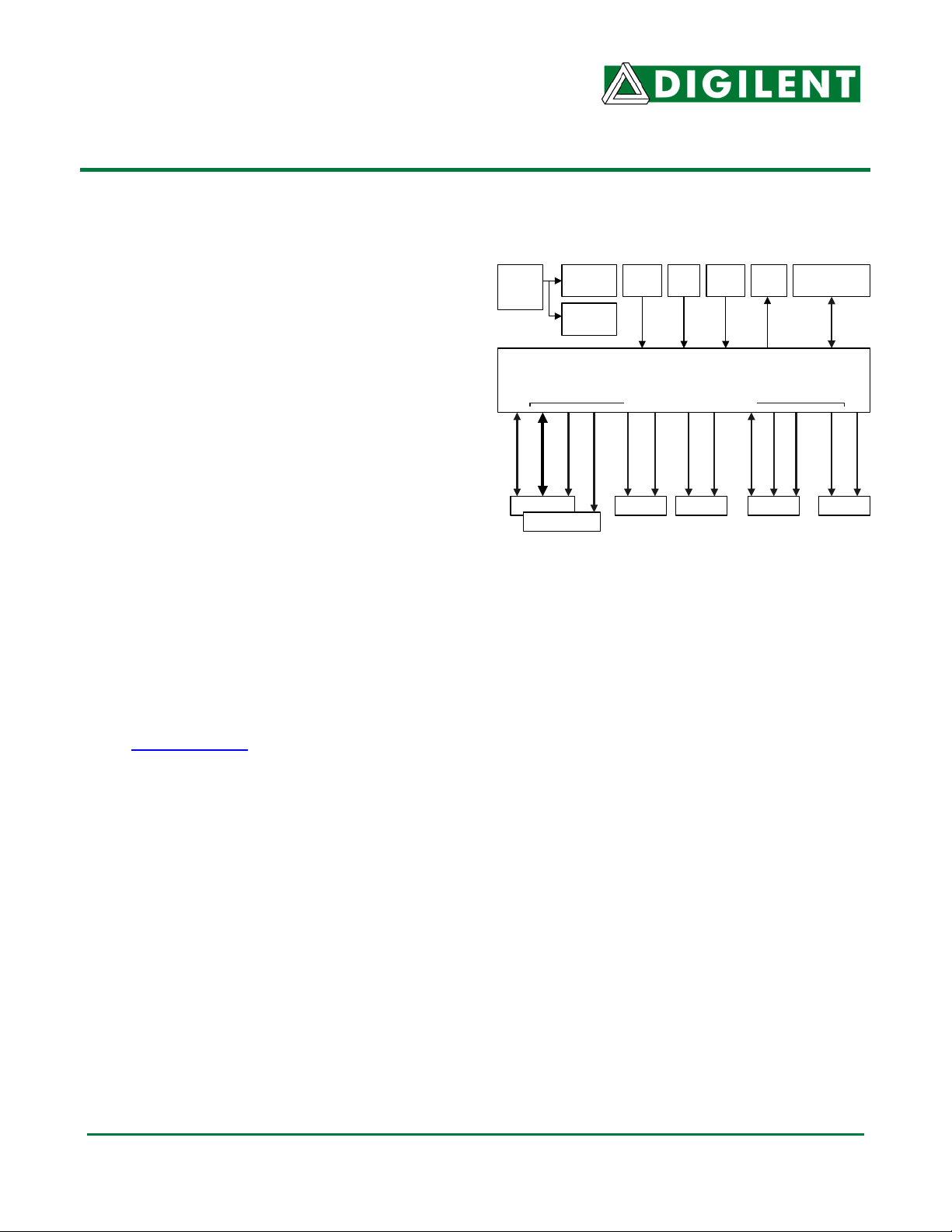
Functional Description
The Digilab D2-FT provides a minimal system
that can be used to rapidly implement FPGAbased circuits, or to gain exposure to Xilinx
CAD tools and Spartan 2E devices. The D2-FT
provides only the essential supporting devices
for the Spartan 2E FPGA, including clock
sources and power supplies. All available I/O
signals are routed to standard expansion
© Digilent, Inc. 7 pages Doc: 502-036
PA bus
ND
2
Clock
MB2 bus
Push
button
PB bus
Status
Configuration
LED
(flash) ROM
JTAG
PC1 bus
MC1 bus
C1 C2
JTAG
MC2 bus
Power
jack
5-9VDC
1.8VDC
regulator
3.3VDC
regulator
Xilinx Spartan2E XC2S300E-FT256
JTAG
MA1 bus
System Bus
A1 B2
MB1 bus
B1
Clock
(50MHz)
Expansion Connectors
MA2 bus
A2
Figure 1. D2-FT Circuit Board Block Diagram
connectors that mate with 40-pin, 100 mil
spaced DIP headers available from any
catalog distributor. A pushbutton and LED are
also included for basic I/O.
The D2-FT board has been designed to serve
primarily as a host for peripheral boards. Each
of the six expansion connectors provides the
unregulated supply voltage (VU), 3.3V, GND,
and 32 I/O signals from the FPGA. Because
there are more connector pins than FPGA
pins, the A1 and B1 connectors share an 18pin bus. All other connector positions are
driven by individual FPGA signals. JTAG
signals are also routed to the A1, B1, and C1
expansion connectors. This allows peripheral
boards to drive the scan chain, or to be
configured along with the Spartan 2E FPGA.
Application-specific peripheral boards can be
created to mate with the D2-FT, or ready-made
peripheral boards that offer many standard I/O
and data port functions can be obtained from
Digilent (for a current listing of available
boards, see www.digilentinc.com).
PC2 bus
Page 2
D2-FT Reference Manual Digilent, Inc.
JTAG Scan Chain and Device Configuration
The Spartan 2E FPGA, the 18V00 ROM on the
D2-FT, and any programmable devices on
peripheral boards attached to the D2-FT can
be programmed via their JTAG ports. The
JTAG scan chain is routed to the FPGA, the
ROM, and around the board to four connection
ports as shown in Figure 2 below. The primary
configuration port (Port 1) uses a standard 6pin JTAG header (J7) that can accommodate
Digilent’s JTAG3 cable (or cables from Xilinx or
other vendors). The other three JTAG
programming ports are bi-directional, and they
are available on the A1, B1, and C1 expansion
connectors. If no peripheral board is present, a
buffer on the D2-FT removes the expansion
connector from the JTAG chain. If a peripheral
board with a JTAG device is attached, the scan
chain is driven out the expansion connector so
that any JTAG-programmable parts can be
configured. If a Digilent port module is
connected to one of the three JTAG-enabled
expansion connectors, then the port module
can drive the JTAG chain to program all
devices in the scan chain (port modules
include Ethernet, USB, EPP parallel, and serial
modules -- see www.digilentinc.com
for more
information).
The scan chain can be driven from the primary
port by powering on the D2-FT, connecting it to
a PC with a JTAG programming cable, and
running the “auto-detect” feature of the
configuration software. The configuration
software allows devices in the scan chain to be
selectively programmed with any available
configuration file. If no programming ROM is
loaded in the IC5 socket (or if ROM is present
but is not to be included in the scan chain),
jumper-shunts must be loaded at JP1 and JP2
in the “Bypass ROM” location to route the
JTAG chain around the ROM socket. If an
18V02 (or larger) ROM is loaded in the IC5
socket, it can be included in the scan chain by
loading the JP1 and JP2 jumper-shunts in the
“Include ROM” positions.
If a programming ROM is present in the IC5
socket, the FPGA will automatically access the
ROM for configuration data if jumper shunts
are loaded in all three positions of J8 (M2, M1,
and M0).
Port modules attached to ports A1, B1, or C1
can drive the scan chain if a jumper-shunt is
installed on the primary JTAG header across
the TDI and TDO pins. In their default state,
Digilent port modules will appear as a JTAG
cable to the configuration software. Port
modules can disable their JTAG drivers; if
more than one JTAG driver is enabled on the
scan chain, programming may fail.
Port 2
ROM bypass
jumpers
JTAG
connector
Cable bypass
jumper
Programming
mode select
jumpers
A1
18V
ROM
Port 1
C2
A2
B1 B2
Spartan 2E
FT 256
C1
Port 4
Figure 2. JTAG Signal Routing on D2-FT
Power Supplies
The D2-FT board uses two LM317 voltage
regulators to produce a 1.8VDC supply for the
Spartan 2E core, and 3.3VDC supply for the
I/O ring. Both regulators have good bypass
capacitance, allowing them to supply up to
1.5A of current with less than 50mV of noise
(typical). Power can be supplied from a lowcost wall transformer supply. The external
supply must use a 2.1mm center-positive
connector, and it must produce between 6VDC
and 12VDC of unregulated voltage.
The D2-FT uses a four layer PCB, with the
inner layers dedicated to VCC and GND
planes. Most of the VCC plane is at 3.3V, with
an island under the FPGA at 1.8V. The FPGA
and the other ICs on the board all have
0.047uF bypass capacitors placed as close as
possible to each VCC pin.
Port 3
www.digilentinc.com © Digilent, Inc. Page 2
Page 3

D2-FT Reference Manual Digilent, Inc.
Total board current is dependant on FPGA
configuration, clock frequency, and external
connections. In test circuits with roughly 50K
gates routed, a 50MHz clock source, and a
single expansion board attached (the DIO5
board), approximately 200mA +/- 30% of
supply current is drawn from the 1.8V supply,
and approximately 200mA +/- 50% is drawn
from the 3.3V supply. These currents are
strongly dependent on FPGA and peripheral
board configurations.
All FPGA I/O signals use the VCCO voltage
derived from the 3.3V supply. If other VCCO
voltages are required, the regulator output can
be modified by changing R12 according to:
VCCO = 1.25(1 + R12/R11).
Refer to the LM317 data sheet and D2-FT
schematic for further information.
Oscillators
The D2-FT provides a 50MHz SMD primary
oscillator and a socket for a second oscillator.
The primary oscillator is connected to the
GLK2 input of the Spartan 2E (pin B8), and the
secondary oscillator is connected to GCLK3
(pin C8). Both clock inputs can drive the DLL
on the Spartan 2E, allowing for internal
frequencies up to four times higher than the
external clock signals. Any 3.3V oscillator in a
half-size DIP package can be loaded into the
secondary oscillator socket.
Pushbutton and LED
A single pushbutton and LED are provided on
the board allowing basic status and control
functions to be implemented without a
peripheral board. As examples, the LED can
be illuminated from a signal in the FPGA to
verify that configuration has been successful,
and the pushbutton can be used to provide a
basic reset function independent of other
inputs. The circuits are shown in Figure 3.
Vdd
Push
button
4.7K
4.7K
80 Ohm
Pin A12
Xilinx
Spartan 2E
FT 256
Pin C15
Figure 3. LED and Pushbutton Circuit
Expansion Connectors
The six expansion connectors labeled A1-A2,
B1-B2, and C1-C2 use 2x20 right-angle
headers with100 mil spacing. All six
connectors have GND on pin 1, VU on pin 2,
and 3.3V on pin 3. Pins 4-35 route to FPGA I/O
signals, and pins 36-40 are reserved for JTAG
and/or clock signals. (See Figure 4)
The expansion headers provide 192 signal
connections, and the Spartan 2E-FT256 has
172 available I/O signals. Thus, some FPGA
signals are routed to more than one connector.
The lower 18 pins (pins 4-21) of the A1and B1
connectors are connected to the same 18
FPGA pins, and they are designated as the
“system bus” (a unique chip select signal is
routed to each connector). Other than these 18
shared signals, all remaining FPGA signals are
routed to individual expansion connector
positions.
The lower 18 pins of the A2, B2, and C2
connectors are designated as “peripheral
busses”, and each of these busses (named
PA, PB, and PC) use 18 unique signals. The
14 upper pins of each expansion connector
(pins 22-35) have been designated as “module
busses”. Each connector has a fully populated
module bus (named MA1, MA2, MB1, MB2,
MC1, and MC2).
System Bus
The “system bus” is a protocol used by certain
expansion boards that mimics a simple 8-bit
microprocessor bus. It uses eight data lines,
six address lines, a write-enable (WE) strobe
that can be used by the peripheral to latch
www.digilentinc.com © Digilent, Inc. Page 3
Page 4

D2-FT Reference Manual Digilent, Inc.
written data, an output-enable (OE) strobe that
can be used by the peripheral to enable read
data, a chip select, and a clock to enable
synchronous transfers. System bus timings
can be used to configure the lower 18 pins of
the A1, B1, and C1 connectors (the lower 18
Write Cycle
CS
tdoe
OE
WE
DB0-DB7
ten
pins of A1 and B1 share the same FPGA pins).
The diagrams below show signal timings
assumed by Digilent to create peripheral
devices. However, any bus and timing models
can be used by modifying circuits in the FPGA
and attached peripheral devices.
th
teoe
tw
tsu
th
Read Cycle
OE
WE
DB0-DB7
Symbol Parameter Time (typ)
teoe
twd
tsu
Figure 4. System Bus Timing
Table 1. System Bus Timing
ten Time to enable after CS asserted 10ns
th Hold time 1ns
tdoe Time to disable after OE de-asserted 10ns
teoe Time to enable after OE asserted 15ns
tw Write strobe time 10ns
tsu Data setup time 5ns
twd Write disable time 0ns
tdoe
th
th
Read data latch time
www.digilentinc.com © Digilent, Inc. Page 4
Page 5

D2-FT Reference Manual Digilent, Inc.
pins 4 -21
A1
pins 22 -35 pins 4 -21 pins 22 -35
A2
pins 4 -21
MA1 (14)
PA(18)
JTAG
Sys Bus (18)
Spartan 2E
FT 256
MA2(14)
MB1(14)
PB(18)
B1
pins 22 -35 pins 4 -21 pins 22 -35
B2
MC2(14)
PC(18)
MC1(14)
PC-SB(14)
MB2(14)
Figure 5. Expansion Connector Signal Routing
C2
pins 4 -21pins 22 -35
C1
pins 4 -21pins 22 -35
Pin 39
Pin 3: 3.3V
Pin 1: GND
Pin 39
Pin 40
Figure 6. Expansion Connector Pin Locations
Pin 4
Pin 2: VU
Pin 40
www.digilentinc.com © Digilent, Inc. Page 5
Page 6

D2-FT Reference Manual Digilent, Inc.
Table 2. D2-FT Expansion Connector Pinout
Pin #
1
2
3
4
5
6
7
8
9
10
11
12
13
14
15
16
17
18
19
20
21
22
23
24
25
26
27
28
29
30
31
32
33
34
35
36
37
38
39
40
A1 A2 B1 B2 C1 C2
Signal
GND GND GND GND GND GND
VU VU VU VU VU VU
VCC33 VCC33 VCC33 VCC33 VCC33 VCC33
ADR0 J14 PAI01 B12 ADR0 J14 PBI01 M10 PCADR0 N3 PCI01 F2
DB0 K16 PAI02 C12 DB0 K16 PBI02 R11 PCDB0 P2 PCI02 E1
ADR1 K13 PAI03 A13 ADR1 K13 PBI03 P10 PCADR1 L5 PCI03 F4
DB1 K15 PAI04 D12 DB1 K15 PBI04 T10 PCDB1 N1 PCI04 E2
ADR2 K14 PAI05 B13 ADR2 K14 PBI05 N10 PCADR2 M3 PCI05 E3
DB2 L16 PAI06 A14 DB2 L16 PBI06 P9 PCDB2 N2 PCI06 D1
ADR3 K12 PAI07 E11 ADR3 K12 PBI07 R10 PCADR3 L4 PCI07 F5
DB3 L15 PAIO8 C16 DB3 L15 PBI08 N9 PCDB3 M1 PCI08 D2
ADR4 L14 PAI09 E13 ADR4 L14 PBI09 N8 PCADR4 L3 PCI09 D3
DB4 M16 PAI010 D14 DB4 M16 PBI010 R9 PCDB4 M2 PCI010 C1
ADR5 L13 PAI011 D16 ADR5 L13 PBI011 P8 PCADR5 K5 PCI011 E4
DB5 M15 PAI012 F12 DB5 M15 PBI012 R8 PCDB5 L1 PCI012 A3
WE M14 PAI013 D15 WE M14 PBI013 N7 PCWE K3 PCI013 C2
DB6 N16 PAI014 E14 DB6 N16 PBI014 T7 PCDB6 L2 PCI014 B3
OE L12 PAI015 E16 OE L12 PBI015 P7 PCOE K4 PCI015 C4
DB7 N15 PAI016 F13 DB7 N15 PBI016 R7 PCDB7 K1 PCI016 A4
CSA D8 PAI017 E15 CSB N14 PBI017 M7 PCCS J3 PCI017 DS
LSBCLK P16 PAI018 F14 LSBCLK P16 PBI018 T6 PCCLK K2 PCI018 B4
MA1DB0 D9 MA2DB0 F16 MB1DB0 M13 MB2DB0 P6 MC1DB0 J4 MC2DB0 C5
MA1DB1 A9 MA2DB1 G12 MB1DB1 T14 MB2DB1 R6 MC1DB1 J1 MC2DB1 A5
MA1DB2 C9 MA2DB2 F15 MB1DB2 N12 MB2DB2 N6 MC1DB2 J2 MC2DB2 E6
MA1DB3 B9 MA2DB3 G14 MB1DB3 R14 MB2DB3 T5 MC1DB3 H4 MC2DB3 B5
MA1DB4 D10 MA2DB4 G16 MB1DB4 P13 MB2DB4 P5 MC1DB4 H1 MC2DB4 C6
MA1DB5 A10 MA2DB5 G13 MB1DB5 T13 MB2DB5 R5 MC1DB5 H3 MC2DB5 A6
MA1DB6 C10 MA2DB6 G15 MB1DB6 M11 MB2DB6 M6 MC1DB6 H2 MC2DB6 D6
MA1DB7 B10 MA2DB7 H14 MB1DB7 R13 MB2DB7 T4 MC1DB7 G4 MC2DB7 B6
MA1ASTB E10 MA2ASTB H16
MA1DSTB A11 MA2DSTB H13
MA1WRT C11 MA2WRT H15 MB1WRT N11 MB2WRT N5 MC1WRT G2 MC2WRT D7
MA1WAIT B11 MA2WAIT J16 MB1WAIT R12
MA1RST D11 MA2RST J13 MB1RST P11
MA1INT A12 MA2INT J15 MB1INT T11 MB2INT P1 MC1INT F3 MC2INT A8
JTSELA JTSELB JTSELC
TMS TMS TMS
TCK TCK TCK
TDOA CLK0 T9 TDOB TDOC CLK1 T8
TDIA GND TDIB TDIC GND
FPGA
Pin
Signal
FPGA
Pin
Signal
MB1AST
MB1DST
FPGA
Pin
P12
T12 MB2DST R4 MC1DSTB G3 MC2DSTB A7
Signal
MB2AST
MB2WAIT
MB2RST
FPGA
Pin
P4 MC1ASTB G1 MC2ASTB C7
T3 MC1WAIT G5 MC2WAIT E7
M4 MC1RST F1 MC2RST B7
Signal
FPGA
Pin
Signal
FPGA
Pin
www.digilentinc.com © Digilent, Inc. Page 6
Page 7

D2-FT Reference Manual Digilent, Inc.
Table 3. D2-FT FPGA Pin Assignments
A B C D E F G H J K L M N P R T
PC-
PC-
PC-
PC-
MC1-
MC1-
1
2
3
4
5
6
7
8
9
10
GND
TMS
IO10
GND
TCK
PC-
IO12
PC-
IO16
MC2-
DB1
MC2-
DB5
MC2-
DSTB
MC2-
GCK2 GCK3 CSA VCCO VCCO GND GND GND GND VCCO VCCO
INT
MA1-
DB1
MA1-
DB5
PC-
IO14
PC-
IO18
MC2-
DB3
MC2-
DB7
MC2-
RST
MA1-
DB3
MA1-
DB7
IO13
VCCI
IO15
MC2-
MC2-
MC2-
ASTB
MA1-
MA1-
PC-
PC-
DB0
DB4
DB2
DB6
IO6
IO2
RST
ASTB
PC-
PC-
PC-
IO8
IO4
PC-
PC-
IO9
IO5
VCCI
IO17
MC2-
MC2WRT
MA1-
MA1-
PC-
IO11
PC-
VCCI
MC2-
DB6
DB2
MC2-
VCCO GND GND GND GND VCCO
WAIT
VCCO VCCO GND GND GND GND VCCO VCCO
DB0
MA1-
DB4
VCCO GND GND GND GND VCCO
ASTB
MC1-
IO1
WRT
MC1-
MC1-
INT
DSTB
PC-
MC1-
IO3
DB7
PC-
MC1-
WAIT
VCCO VCCO
IO7
GND VCCO VCCO VCCO VCCO GND
DB4
MC1-
DB6
MC1-
DB5
MC1-
DB3
MC1-
DB1
MC1-
DB2
MC1-
MC1-
D80
CS
PC-
DB7
PC-
CLK
PCWE
PCOE
PC-
ADR5
PC-
DB5
PC-
DB6
PC-
ADR4
PC-
ADR3
PC-
ADR1
PC-
DB3
PC-
DB4
PC-
ADR2
MB2-
RST
VCCI
MB2-
DB6
PB-
IO17
PBIO1
PC-
DB1
PCDB2
PC-
ADR0
VCCI
MB2WRT
MB2-
DB2
PB-
IO13
PBIO9
PBIO8
PBIO5
MB2-
INT
PC-
DB0
VCCI
MB2ASTB
MB2-
DB4
MB2-
DB0
PB-
IO15
PB-
IO11
PBIO6
PBIO3
M1
GND
M2
MB2-
DSTB
MB2-
DB5
MB2-
DB1
PB-
IO16
PB-
IO12
PB-
IO10
PBIO7
GND
M0
MB2WAIT
MB2-
DB7
MB2-
DB3
PB-
IO18
PB-
IO14
GCK1
GCK0
PBIO4
MA1-
MA1-
MA1-
11
12
13
14
15
16
DSTB
WAIT
MA1-
BTN
CCLK
GND D0
INT
PAIO3
PAIO6
PAIO1
PAIO5
TDO
GND LED
WRT
PAIO2
TDI
VCCI
PAIO8
MA1-
VCCI
IO10
IO13
IO11
RST
PAIO4
PA-
PA-
PA-
PA-
GND VCCO VCCO VCCO VCCO GND
IO7
PA-
IO12
PA-
IO16
PA-
IO18
MA2-
DB2
MA2-
DB0
MA2-
VCCO VCCO ADR3 OE VCCI
DB1
MA2-
MA2-
DB5
MA2-
DB3
MA2-
DB6
MA2-
DB4
MA2-
DSTB
ASTB
RST
MA2-
ADR0 ADR2 ADR4 WE CSB VCCI
DB7
MA2-
MA2-
WRT
MA2-
INT
MA2-
WAIT
VCCI
PA-
IO9
PA-
IO14
PA-
IO17
PA-
IO15
MB1-
MB1-
DB6
WRT
MB1-
DB2
ADR1 ADR5
DB1 DB3 DB5 DB7
DB0 DB2 DB4 DB6
MB1-
DB0
VCCI
MB1-
RST
MB1ASTB
MB1-
DB4
OE/
RST
LDB
CLK
PBIO2
MB1-
WAIT
MB1-
DB7
MB1-
DB3
GND CE
CF GND
MB1-
INT
MB1-
DSTB
MB1-
DB5
MB1-
DB1
www.digilentinc.com © Digilent, Inc. Page 7
 Loading...