

Page 1
1300 Henley Court
Pullman, WA 99163
509.334.6306
www.digilentinc.com
chipKIT™ WF32™ Board Reference Manual
Revised September 16, 2013
This manual applies to the chipKIT WF32 rev. B
DOC#: 502-273
Copyright Digilent, Inc. All rights reserved.
Other product and company names mentioned may be trademarks of their respective owners.
Page 1 of 24
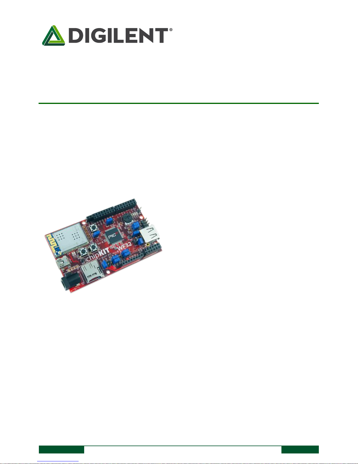
The chipKIT WF32 board.
Microchip® PIC32MX695F512L microcontroller (80
MHz 32-bit MIPS, 512K Flash, 128K SRAM)
Microchip MRF24WG0MA WiFi module
microSD card connector
USB 2.0 OTG controller with A and micro-AB
connectors
43 available I/O pins
Four user LEDs
PC connection uses a USB A to mini-B cable (not
included)
12 analog inputs
3.3V operating voltage
80 MHz operating frequency
7V to 15V input voltage (recommended)
30V input voltage (maximum)
0V to 3.3V analog input voltage range
High efficiency, switching 3.3V power supply
providing low-power operation
Overview
The chipKIT WF32 is based on the popular Arduino™ open-source hardware prototyping platform and adds the
performance of the Microchip PIC32 microcontroller. The WF32 is the first board from Digilent to have a WiFi
MRF24 and SD card on the board both with dedicated signals. The WF32 board takes advantage of the powerful
PIC32MX695F512L microcontroller. This microcontroller features a 32-bit MIPS processor core running at 80Mhz,
512K of flash program memory, and 128K of SRAM data memory.
The WF32 can be programmed using the Multi-Platform Integrated Development Environment (MPIDE), an
environment based on the original Arduino IDE, modified to support PIC32. It contains everything needed to start
developing embedded applications. The WF32 features a USB serial port interface for connection to the MPIDE and
can be powered via USB or by an external power supply. In addition, the WF32 is fully compatible with the
advanced Microchip MPLAB® IDE and works with all MPLAB compatible in-system programmer/debuggers, such as
the Microchip PICkit™3 or the Digilent chipKIT PGM. The WF32 is easy to use and suitable for both beginners and
advanced users experimenting with electronics and embedded control systems.
Page 2
chipKIT™ WF32™ Board Reference Manual
Copyright Digilent, Inc. All rights reserved.
Other product and company names mentioned may be trademarks of their respective owners.
Page 2 of 24
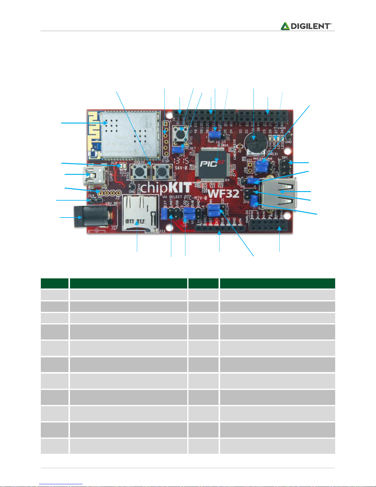
1
3
2
4
5 6
7
8
9
10
11
12
13
14
16
15
17
18
19
20
21
22
23
24
25
26
27
28
29
Call Out
Component Description
Call Out
Component Description
1
IC3- Microchip MRF24WG0MA WiFi Module
16
J13- USB Connectors
2
User Buttons
17
JP9- USB Overcurrent Detect
3
JP3- Microchip Debug Tool Connector
18
JP11- Hos USB Bus Power Enable
4
J6- Signals
19
J8- Analog and Digital Signal Connector
5
BTN1- Reset
20
JP5, JP4- Analog or C Select Jumper
6
JP1- Reset Disable
21
J3- Shield Power Connector
7
J9- Digital Signal Connector
22
J16- 5.0V Supply Select
8
JP3- Pin 10 Signal Select Jumper
23
J15- Power Select Jumper
9
PIC32 Microcontroller
24
J11- Micro SD Connector
10
Potentiometer
25
J17- External Power Connector
11
J7- Digital Signal Connector
26
J14- External Power Connector
1 ChipKIT WF32 Hardware Overview
The WF32 has the following hardware features:
Page 3

chipKIT™ WF32™ Board Reference Manual
Copyright Digilent, Inc. All rights reserved.
Other product and company names mentioned may be trademarks of their respective owners.
Page 3 of 24
12
User LEDs
27
J2- USB- UART Handshaking Signals
13
JP6,7- SPI Master/ SPI Slave Select
28
USB connector for USB Serial Converter
14
J10- SPI Connector
29
Serial Communication LEDs
15
JP10- USB Host or OTG Select
2 MPIDE and USB Serial Communications
The WF32 board is designed to be used with MPIDE. The MPIDE development platform was created by modifying
the Arduino IDE. It is backwards-compatible with the Arduino IDE. Links for where to obtain the MPIDE installation
files and instructions for installing MPIDE can be found at www.chipkit.net/started.
The MPIDE uses a serial communications port to communicate with a boot loader running on the WF32 board. The
serial port on the WF32 board is implemented using an FTDI FT232RQ USB serial converter. Before attempting to
use the MPIDE to communicate with the WF32, the appropriate USB device driver must be installed.
The WF32 board uses a standard mini-USB connector. Generally, a USB A to mini-B cable is used for connection to
a USB port on the PC.
When the MPIDE needs to communicate with the WF32 board, the board is reset and starts running the boot
loader. The MPIDE then establishes communications with the boot loader and uploads the program to the board.
When the MPIDE opens the serial communications connection on the PC, the DTR pin on the FT232RQ chip is
driven low. This pin is coupled through a capacitor to the MCLR pin on the PIC32 microcontroller. Driving the MCLR
line low resets the microcontroller, which restarts the execution with the boot loader.
This automatic reset action (when the serial communications connection is opened) can be disabled. To disable
this operation, there is a jumper labeled JP1, which can be disconnected. JP1 is normally shorted, but if the
shorting block is removed, the automatic reset operation will be disabled.
Two red LEDs (LD1 and LD2) will blink when data is being sent or received between the WF32 and the PC over the
serial connection.
The header connector J2 provides access to the other serial handshaking signals provided by the FT232RQ.
Connector J2 is not loaded at the factory and can be installed by the user to access these signals.
3 Power Supply
The WF32 is designed to be powered via USB (J1), from an external power supply (J14 or J17), or from the USB OTG
receptacle (J12). Jumper block J15 is used to select which power supply is used. The power supply voltage selected
by J15 is applied to the unregulated power bus, VU.
In order to operate the WF32 as a USB device powered from the USB serial interface, connector J1, place a
shorting block in the UART position of jumper block J15. To operate the WF32 from an external power supply,
Page 4

chipKIT™ WF32™ Board Reference Manual
Copyright Digilent, Inc. All rights reserved.
Other product and company names mentioned may be trademarks of their respective owners.
Page 4 of 24
LDO OutLDO In
VU 5V0
GNDEN Ext
attach the power supply to either J14 or J17 and place a shorting block in the EXT position of J15. Be sure to
observe correct polarity when connecting a power supply to J14, as a reversed connection could damage the
board. To operate the WF32 as a USB powered device from the USB OTG connector (J12) place a shorting block on
the USB position of J15. This will normally only be done when running a sketch on the board that programs it to
operate as a USB device. The power supply section in the WF32 provides two voltage regulators, a 3.3V regulator
and a 5V regulator. All systems on the WF32 board itself operate at 3.3V and are powered by the 3.3V regulator.
The 5V regulator is used to provide power for external circuits, such as shields, that require 5V for operation. The
5V regulator can be completely disabled if it is not needed for a given application.
The WF32 board is designed for low power operation and efficient use of battery power, as such a switch mode
voltage regulator is used for the 3.3V power supply. This switch mode regulator is made up of a Microchip
MCP16301 and associated circuitry. It can operate on input voltages from 4V to 30V with up to 96% efficiency, and
is rated for 600mA total current output. The MCP16301 has internal short circuit protection and thermal
protection. The 3.3V regulator takes its input from the unregulated power bus, VU, and produces its output on the
VCC3V3 power bus. The VCC3V3 bus provides power to all on-board systems and is available at the shield power
connector (J3) to provide 3.3V power to external circuitry, such as shields.
The 5V regulator section provides a low dropout linear regulator. No circuitry on the WF32 board uses the 5V
supply. It is provided for powering external circuitry that needs a 5V power supply. This voltage regulator uses an
On Semiconductor NCP1117LP. The NCP1117LP is rated for an output current of 1A. The dropout voltage of the
NCP1117LP is a maximum of 1.4V at 1A output current. The maximum input voltage of the NCP1117LP is 18V. The
recommended maximum operating voltage is 15V.
The input voltage to the 5V regulator section is taken from the VU bus, and the output is placed on the VCC5V0
power bus.
There is a reverse polarity protection diode in the external power supply circuit. Considering the diode drop plus
the forward drop across the regulator, the minimum input voltage to the regulator should be 7V to produce a
reliable 5V output.
For input voltages above 9V, the regulator will get extremely hot when drawing high currents. The NCP1117LP has
output short circuit protection and internal thermal protection and will shut down automatically to prevent
damage.
The 5V regulator section actually provides four 5V power options:
1) 5V regulator completely disabled and no 5V power available;
2) 5V regulator bypassed and 5V provided from an external 5V power supply, such as USB;
3) on-board 5V regulator used to provide 5V power;
4) External 5V regulator used to regulate VU and provide 5V power.
Jumper block J16 is used to select these various options and the following diagrams describe the use of J16:
This diagram shows the arrangement of the signals on J16:
LDO In is the input to the on-board linear regulator.
LDO Out is the output of the on-board linear regulator
Page 5
chipKIT™ WF32™ Board Reference Manual
Copyright Digilent, Inc. All rights reserved.
Other product and company names mentioned may be trademarks of their respective owners.
Page 5 of 24
LDO OutLDO In
VU 5V0
GNDEN Ext
LDO OutLDO In
VU 5V0
GNDEN Ext
VU is the unregulated input voltage selected by the jumper setting jumper block J15.
5V0 is the connection to the VCC5V0 power bus on the WF32 board.
EN Ext is a signal provided to enable an external voltage regulator if one is being used. This would allow the sketch
running on the WF32 to turn on/off the external voltage regulator. When used with an external voltage regulator,
this allows the board to go into an extremely low power operating mode. This signal is connected to Port D, bit 13
(RD13) on the PIC32 microcontroller. This is accessible using digital pin 64.
GND is a connection to the digital ground bus on the WF32 board.
To completely disable operation of the on-board linear regulator, remove all shorting blocks from J16.
To use the on-board 5V regulator, use the provided shorting blocks to connect VU to LDO In, and to connect LDO
Out to 5V0, as follows:
Note: In this case, when J15 is in the EXT position, and J16 is jumpered to regulate the external input, do not apply
more than 18V. This can destroy the 5.0V regulator.
To bypass the on-board 5V regulator when powering the board from an externally regulator 5V power supply, such
as USB, Use one of the provided shorting blocks to connect VU to 5V0, as follows:
An external 5V regulator can be used. This would be desirable, for example, when operating from batteries. An
external switch mode 5V regulator could be used to provide higher power efficiency than the on-board linear
regulator. In this case, use wires as appropriate to connect VU to the unregulated input of the external regulator.
Connect the regulated 5V output to 5V0. Connect GND to the ground connection of the external regulator.
Optionally, connect EN Ext to the enable input control of the external regulator, if available. This allows the
external regulator to be turned off for low power operation. Digital pin 64 is then used to turn on/off the external
regulator.
The PIC32MX695 microcontroller is rated to use a maximum of 98mA of current when operating at 80Mhz. The
MRF24WG0MA WiFi module typically consumes a maximum of 237mA when transmitting. This allows
approximately 265mA of current to power the remaining 3.3V circuitry on the WF32 board and external circuitry
powered from the VCC3V3 bus. No circuitry on the WF32 board is powered from the VCC5V0 power bus, leaving
all current available from the 5V regulator to power external circuitry.
The POWER connector (J3) is used to power shields connected to the WF32 board. Pin 1 is unconnected, the
following pins are provided on this connector:
IOREF (pin 2): This pin is tied to the VCC3V3 bus.
P32_RST (pin 3): This connects to the MCLR pin on the PIC32 microcontroller and can be used to reset the PIC32.
VCC3V3 (pin 4): This routes the 3.3V power bus to shields.
VCC5V0 (pin 5): This routes the 5V power bus to shields.
Page 6

chipKIT™ WF32™ Board Reference Manual
Copyright Digilent, Inc. All rights reserved.
Other product and company names mentioned may be trademarks of their respective owners.
Page 6 of 24
GND (pin 6, 7): This provides a common ground connection between the WF32 and the shields. This common
ground is also accessible on connectors J4 and J5.
VEXT (pin 8): This connects to the voltage provided at the external power supply connectors (J14 and J17). This
can be used to provide unregulated input power to the shield. It can also be used to power the WF32 board from
the shield instead of from the external power connector.
4 5V Compatibility
The PIC32 microcontroller operates at 3.3V. The original Arduino boards operate at 5V, as do many Arduino
shields.
There are two issues to consider when dealing with 5V compatibility for 3.3V logic. The first is protection of 3.3V
inputs from damage caused by 5V signals. The second is whether the 3.3V output is high enough to be recognized
as a logic high value by a 5V input.
The digital I/O pins on the PIC32 microcontroller are 5V tolerant. The analog capable I/O pins are not 5V tolerant.
To provide 5V tolerance on those pins, the WF32 contains clamp diodes and current limiting resistors to protect
them from 5V input voltages.
The fact that all I/O pins are 5V tolerant means that it is safe to apply 5V logic levels to any pins on the board
without risk of damaging the PIC32 microcontroller.
The minimum high-voltage output of the PIC32 microcontroller is rated at 2.4V when sourcing 12mA of current.
When driving a high impedance input (typical of CMOS logic) the output high voltage will be close to 3.3V. Some 5V
devices will recognize this voltage as a logic high input, and some won’t. Many 5V logic devices will work reliably
with 3.3V inputs.
5 Input/ Output Connections
The WF32 board provides 43 of the I/O pins from the PIC32 microcontroller at pins on the input/output connectors
J6, J7, J8, J9, and J10.
The PIC32 microcontroller can source or sink a maximum of 25mA on all digital I/O pins. However, to keep the
output voltage within the specified output voltage range (VOL 0.4V, VOH 2.4V) the pin current must be restricted to
+7/-12mA. The maximum current that can be sourced or sunk across all I/O pins simultaneously is +/-200mA. The
maximum voltage that can be applied to any I/O pin is 5.5V although not all pins are 5V tolerant. For more detailed
specifications, refer to the PIC32MX5XX/6XX/7XX Data Sheet available from www.microchip.com.
Note that the series resistors that are part of the voltage clamp circuit to provide 5V tolerance on the analog
capable I/O pins, limiting the current that can be sourced or sunk by those pins. These resistors add 200 ohms of
resistance to the input/output circuit and limit the effective drive current to about 1mA-2mA source/sink capability
on the analog capable pins.
Connectors J7 and J9 are 2x8 female pin header connectors that provide digital I/O signals. The outer row of pins
(closer to the board edge) corresponds to the I/O connector pins on an Arduino Uno or Duemilanove board. The
inner row of pins provides access to the extra I/O signals provided by the PIC32 microcontroller.
Connector J8 is a 2x6 female pin header connector that provides access to the analog input pins on the
microcontroller. The outer row of pins corresponds to the six analog pins on an Arduino Uno or Duemilanove. The
inner row of pins is for the additional I/O signals provided by the PIC32 microcontroller. The analog pins on J8 can
also be used as digital I/O pins.
Page 7

chipKIT™ WF32™ Board Reference Manual
Copyright Digilent, Inc. All rights reserved.
Other product and company names mentioned may be trademarks of their respective owners.
Page 7 of 24
The chipKIT/Arduino system uses logical pin numbers to identify digital I/O pins on the connectors. The logical pin
numbers for the I/O pins on the WF32 are 0-48. These pin numbers are labeled in the silk screen on the board.
Pin numbers 0-13 are the outer row of pins on J9 and J7, from right to left. Pin numbers 14-19 are the outer row of
pins on J8 from left to right. Pins 20-25 are the inner row of pins on J8 from left to right. Pin numbers 26-41 are the
inner row of pins on J9 and J7 from right to left. Pin 42 is the pin labeled A on J7. This pin is normally the reference
voltage for the microcontroller’s A/D converter, but can also be used as a digital I/O pin.
In addition to the connector pin, Pin 13 also connects to the user LED LD3. Pin 43 connects to user LED LD5. Pin 43
does not attach to any connector. Pin 44 is the SS signal for SPI port 2, and discussed more in the SPI section
below. Pins 45 and 46 are intended to be used for I2C and are connected to the 2x1 female header connector, J6.
Pins 47 and 48 connect to the user LEDs LD5 and LD6.
The analog inputs on connector J8 are assigned pin numbers. The outer row of pins on J8 is analog inputs A0-A5.
The inner row of pins is A6-A11. These pins are also assigned digital pin numbers; A0-A5 are digital pins 14-19, and
A6-A11 are 20-25.
6 802.11b/g Interface
The 802.11b/g compatible WiFi interface on the WF32 is provided by a Microchip MRF24WG0MA WiFi module.
This module provides the radio transceiver, antenna, and 802.11 compatible network firmware.
The MRF24WG0MA firmware provides the 802.11 network protocol software support. The DNETcK and DWIFIcK
libraries provide the TCP/IP network protocol support that works with the 802.11 protocol support provided by the
WiFi module.
The primary communications interface with the MRF24WG0MA WiFi module is a 4 wire SPI bus. This SPI bus uses
SPI4 in the PIC32 microcontroller, and this SPI controller is dedicated to use for communications with the WiFi
module.
The WiFi module supports SPI clock speeds up to 25MHz. In addition to the SPI interface, the interface to the WiFi
module also includes a reset signal, an interrupt signal and a hibernate signal. The active low RESET signal is used
to reset the WiFi module The external interrupt signal, INT, is used by the module to signal to the host
microcontroller that it needs servicing by the microcontroller software. The INT signal on the WiFi module is
connected to external interrupt INT4 on the PIC32 microcontroller. The active low HIBERNATE signal is used to
power the WiFi module down and put it into a low power state.
The interface signals to the WiFi module are controlled by the network libraries and are not normally accessed by
the user sketch. Refer to the schematic for the WF32 board for details on these connections.
More detailed information about the operation of the MRF24WG0MA can be obtained from the manufacturer
data sheet available from www.microchip.com.
7 Network Library Software
The WiFi module on the WF32 is intended for use with the Digilent chipKIT network libraries DNETcK and DWIFIcK.
The DNETcK library provides TCP/IP protocol support for all chipKIT compatible network interfaces supported by
Digilent products, including the WF32. The DWIFIcK library provides the additional library support required for
connecting to and operating with the Microchip MRF24WG0MA wireless network modules.
Page 8

chipKIT™ WF32™ Board Reference Manual
Copyright Digilent, Inc. All rights reserved.
Other product and company names mentioned may be trademarks of their respective owners.
Page 8 of 24
The DWIFIcK library supports both the MRF24WB0MA and MRF24WG0MA modules. The correct header file must
be used to specify the network hardware being used by the sketch. When writing a network sketch on the WF32,
use the following hardware library:
#include <WiFiShieldOrPmodWiFi_G.h>
The Digilent chipKIT network libraries are available for download from the Digilent web site: www.digilentinc.com.
These libraries make use of a custom version of the Microchip Application Library. It is necessary to accept the
Microchip Application Library license agreement before downloading the library.
There are reference examples demonstrating the use of these libraries in the library download. There are more
extensive examples available on the Digilent web site as well.
8 USB Interface
The PIC32MX695 microcontroller on the WF32 contains a USB 2.0 Compliant, Full Speed Device and On-The-Go
(OTG) controller. This controller provides the following features:
USB full speed host and device support.
Low speed host support.
USB OTG support.
Endpoint buffering anywhere in system RAM.
Integrated DMA to access system RAM and Flash memory.
Connector J13 on the top right side of the board is a standard USB type A receptacle. This connector will be used
when the WF32 has been programmed to operate as a USB embedded host. The USB device is connected either
directly to the WF32, or via cable to this connector.
Connector J12, on the bottom right side of the board is the Device/OTG connector. This is a standard USB micro-AB
connector. Connect a cable with a micro-A plug (optionally available from Digilent) from this connector to an
available USB port on a PC or USB hub for device operation.
The USB specification allows for two types of devices with regard to how they are powered: self-powered devices
and bus powered devices. A self-powered device is one that is powered from a separate power supply and does
not draw power from the USB bus. A bus powered device is one that draws power from the USB bus and does not
have a separate power supply.
The WF32 can be operated as a self-powered device or as a bus powered device from either the USB serial
connector (J1) or the USB OTG/device connector (J12). As described in the power supply section above, jumper
block (J15) is used to select the power source to be used to power the board.
For operation as a self-powered device, place a shorting block on the EXT position of J15 and connect a suitable
external power supply to either J14 or J17.
To operate the WF32 as a bus powered device powered from the USB serial connector (J1), place a shorting block
in the UART position of J15. To operate as a bus powered device powered from the OTG/device connector (J12),
place a shorting block in the USB position of J15.
Note that there are two completely independent USB interfaces on the WF32 board, and it is possible for the
WF32 to appear as two different USB devices at the same time. These two devices can be connected to two
Page 9

chipKIT™ WF32™ Board Reference Manual
Copyright Digilent, Inc. All rights reserved.
Other product and company names mentioned may be trademarks of their respective owners.
Page 9 of 24
different USB ports on the same host, or to USB ports on two different hosts. If the WF32 board is connected to
two different USB hosts simultaneously, there will be a common ground connection between these two hosts
through the WF32 board. In this case, it is possible for ground current to flow through the WF32 board, possibly
damaging one or the other USB host if they do not share a common earth ground connection.
When the WF32 is operating as a bus powered device using USB connector J1, it will appear as a self-powered
device from the perspective of a USB host connected to J12. Similarly when operating as a bus powered device
from connector J12, it will appear as a self-powered device from the perspective of connector J1.
A USB host is expected to be able to provide bus power to USB devices connected to it. Therefore, when operating
as a USB host, the WF32 should normally be externally powered. Connect a power supply to the external power
connector, J17. It is possible to operate the WF32 as a USB host powered from USB connector J1, however in this
case, the host USB port will be providing power for the WF32 as well as the USB device connected to the WF32. In
this case, ensure that the total load does not exceed the 500mA maximum load that a USB device is allowed to
present to the host.
The USB host provides regulated 5V power to the connected USB device. The internal 5V LDO regulator can be
used to provide the USB power when operating from an external power supply. Place shorting blocks on jumper
block J16 as described above in the power supply section.
If the external power supply being used is a regulated 5V supply, place a shorting block between pins VU and 5V0
on connector J16 as described above in the power supply section.
The power supply used must be able to supply enough current to power both the WF32, and the attached USB
device, since the WF32 provides power to the attached USB device when operating as a host. The USB 2.0
specification requires that the host provide at least 100mA to the device.
Jumper JP10 is used to route power to the host connector being used. Place the shorting block in the “A” position
when using the standard USB type A (host) Connector (J13). Place the shorting block in the “AB” position for use
with the USB micro-AB (OTG) connector (J12).
When operating as a USB host, the PIC32MX695 microcontroller controls application of power to the connected
device via the VBUSON control pin (labeled VBUSON in the schematic). Bus power is applied to the USB bus by
driving the VBUSON pin high. Power is removed from the bus by driving the VBUSON pin low. The VBUSON pin is
accessed via bit 3 of the U1OTGCON register. The VBUSON signal is shared with same microcontroller pin as analog
input A. When operating as a USB host, this pin is not available as an analog input or general purpose I/O pin.
The VBUSON pin drives the enable input of a TPS2051B Current-Limited Power Distribution Switch to control the
application of USB power to the host connector. This switch has over-current detection capability and provides an
over-current fault indication by pulling the signal USBOC low. The over-current output pin can be monitored via
the INT3/RA14 pin on the PIC32MX695 microcontroller. This signal appears on connector J7, pin 1 on the board,
and is chipKIT digital pin 8. Details about the operation of the TPS2051B can be obtained from the data sheet
available at www.ti.com.
Both the VBUSON and the INT3/RA14 signals connect to the TPS2051B through jumpers JP11, and JP9,
respectively. When operating as a USB host, both jumpers should be shorted with shorting blocks. Pin A7 will be
unusable as an analog input and will be driven as an output. To monitor the over-current output pin of the
TPS2051B, us the attachInterrupt() function to set INT3/RA14 (pin 8) as an external interrupt.
The PIC32 USB controller can be accessed using the chipKIT USB libraries for use within the MPIDE environment.
Page 10

chipKIT™ WF32™ Board Reference Manual
Copyright Digilent, Inc. All rights reserved.
Other product and company names mentioned may be trademarks of their respective owners.
Page 10 of 24
When using the WF32 outside the MPIDE environment, the Microchip Application Library provides USB stack code
that can be used with the board. There are reference designs available on the Microchip web site demonstrating
both device and host operation of PIC32 microcontrollers. These reference designs are suitable to use for
developing USB firmware for the WF32 Shield.
9 SD Card Interface
The micro-SD card connector provides the ability to access data stored on micro-SD sized flash memory cards using
the SD card library provided as part of the MPIDE software system.
The SD card is accessed using an SPI interface on PIC32 microcontroller pins dedicated to this purpose. The SD
library uses a ‘bit-banged’ software SPI implementation to talk to SD cards.
On the WF32 board, the I/O pins used to communicate with the SD card are dedicated to that function and not
shared with other uses.
10 Peripheral I/O Functions
The PIC32 microcontroller on the WF32 board provides a number of peripheral functions. The following
peripherals are provided:
10.1 UART Ports
UART 1: Asynchronous serial port. Pin 0 (RX), Pin 1 (TX). This is accessed using the runtime object: Serial. These
pins are connected to I/O connector J9 and are also connected to the FT232RQ USB serial converter. It is possible
to use these pins to connect to an external serial device when not using the USB serial interface. This uses UART1
(U1RX, U1TX) on the PIC32 microcontroller.
UART 4: Asynchronous serial port. Pin 39 (RX), Pin 40 (TX). This is accessed using the runtime object: Serial1. This
uses UART4 (U24X, U4TX) on the PIC32 microcontroller.
10.2 SPI
Synchronous serial port. Pin 10 (SS), Pin 11 (MOSI), Pin 12 (MISO), Pin 13 (SCK).This can be accessed using the SPI
standard library. It can also be accessed using the DSPI0 object from the DSPI standard library. This uses SPI2 (SS2,
SDI2, SDO2, SCK2) on the PIC32 microcontroller. These signals also appear on connector J10.
Jumpers JP6 and JP7 are used to select whether the WF32 operates as a Master (transmit on MOSI, receive on
MISO) or a Slave (transmit on MISO, receive on MOSI) device. The shorting blocks on JP6 and JP7 are normally
placed in the Master position for the WF32 to function as an SPI master.
Jumper JP3 is used to select PWM output or the SPI SS function on Pin 10. The shorting block on JP3 should be in
the PWM position to select PWM output. It should be in the SS position to select the SPI SS function. JP4 will
normally be in the PWM position. In general, the only time it needs to be in the SS position is when the WF32
board is being used as an SPI slave device.
SPI1: Synchronous serial port. This is an additional SPI interface on the PIC32 microcontroller that can be assessed
using the DSPI1 object from the DSPI standard library. It is not accessible using the SPI standard library. Several of
the SPI1 signals are shared in various ways with other peripheral functions. SS1 is connected to connector J9, pin
Page 11

chipKIT™ WF32™ Board Reference Manual
Copyright Digilent, Inc. All rights reserved.
Other product and company names mentioned may be trademarks of their respective owners.
Page 11 of 24
15, the connector location for digital pin 7, via a 1K ohm resistor. This signal is accessed via digital pin number 71.
SDO1 is accessed via digital pin 3. This conflicts with one of the PWM outputs accessed using analogWrite(). SDI1 is
accessed via digital pin 38. SCK1 is connected to connector J7, pin 1, the connector location for digital pin 8, via a
1K ohm resistor. This conflicts with external interrupt INT3. This signal can be accessed via digital pin number 72.
SPI3: Synchronous serial port. This is an additional SPI interface on the PIC32 microcontroller that can be accessed
using the DSPI2 object from the DSPI standard library. It is not accessible using the SPI standard library. Pin 39
(SS3), pin 1 (SDO3), pin 0 (SDI1), and pin 40 (SCK3). Note that pins 0 and 1 conflict with UART1: object class Serial.
Pins 39 and 40 conflict with UART4: Serial1 object class.
SPI4: Synchronous serial port. This port is dedicated for access to the MR24WG0MA WiFi module and is normally
only used by the networking libraries. This can be accessed using the DSPI3 object class from the DSPI standard
library, but this is not recommended for normal operation of the board.
10.3
Synchronous serial interface. The PIC32 microcontroller shares analog pins A4 and A5 with the two I2C signals SDA
and SCL. Jumpers JP4 and JP5 are used to select whether the analog pin functions or the I2C pin functions are
being used. The shorting blocks are placed in the AN position to select the analog input function or general digital
I/O. They are placed in the I2C position to select the I2C function. This uses I2C2 (SDA2, SCL2) on the PIC32
microcontroller. Both SDA2 and SCL2 are accessible on connector J6.
Note: The I2C bus uses open collector drivers to allow multiple devices to drive the bus signals. This means that
pull-up resistors must be provided to supply the logic high state for the signals. These pull-up resistors are 2.2 kiloohms and labeled R18 and R19 on the WF32 board, but they require that chipKIT pin numbers 62 and 63 are driven
to a logic high ('1') level. Code to enable the on-board pullup resistors is as follows:
C
In MPLAB X:
//disables the jtag module
DDPCONbits.JTAGEN = 0;
//Drive RA2 and RA3 to digital high
TRISASET = 0xC;
PORTASET = 0xC;
In MPIDE:
//the jtag module is disabled by default
pinMode(62, OUTPUT);
pinMode(63, OUTPUT);
digitalWrite(62, HIGH);
digitalWrite(63, HIGH);
10.4 PWM
Pulse width modulated output; Pins 3 (OC1), 5 (OC2), 6 (OC3), 9 (OC4), and 10 (OC5). These can be accessed using
the analogWrite() runtime function.
Page 12

chipKIT™ WF32™ Board Reference Manual
Copyright Digilent, Inc. All rights reserved.
Other product and company names mentioned may be trademarks of their respective owners.
Page 12 of 24
10.5 External Interrupts
Pin 3 (INT0), Pin 2 (INT1), Pin 7 (INT2), Pin 8 (INT3), Pin 57 (INT4). Note that the pin numbers for INT0 and INT4 are
different than on some other chipKIT boards. INT4 is dedicated for use with the MRF24WG0MA WiFi module and is
not brought out to a connector pin.
10.6 User LEDs
Pin 13 (LD6), Pin 43 (LD5), Pin 47 (LD4), Pin 48 (LD3). Pin 13 is shared between a connector pin and the LED. Pin 43,
48, and 47 only goes to the LED and not to any connector pin. Driving the pin HIGH turns the LED on, driving it LOW
turns it off.
10.7 User Push Buttons
There are two push button switches labeled BTN2 (pin 65), and BTN3 (pin 66). The digitalRead() function will return
LOW if the button is not pressed and HIGH when the button is pressed.
10.8 A/D Converter Reference
Labeled A, the left-most outer pin on connector J5. This is used to provide an external voltage reference to
determine the input voltage range of the analog pins. The maximum voltage that can be applied to this pin is 3.3V.
This pin can also be used as digital pin 42.
10.9 Potentiometer
A potentiometer (pot) is provided on the board to be used as an analog signal source or analog control input. The
pot is a 10Kohm trimmer pot connected between the VCC3V3 supply and ground. The wiper of the pot is
connected to analog input A13. The pot is read using the analogRead() function.
10.10 RTCC
Real Time Clock Calendar. The PIC32 microcontroller contains an RTCC circuit that can be used to maintain time
and date information. The operation of the RTCC requires a 32.768Khz frequency source. Crystal X2 (not loaded),
just above and to the right of the PIC32 microcontroller IC, is provided for you to solder a 32Khz watch crystal. The
Citizen CFS206-32.768KDZF-UB crystal can be used in this location.
10.11 RESET
The PIC32 microcontroller is reset by bringing its MCLR pin low. The MCLR pin is connected to the P32_RST net on
the circuit board.
As described earlier, reset of the PIC32 microcontroller can be initiated by the USB serial converter. The USB serial
converter brings the DTR pin low to reset the microcontroller. Jumper JP1 can be used to enable/disable the ability
for the USB serial converter to initiate a reset.
The P32_RST net is connected to pin 3 of connector J3. This allows circuitry on a shield to reset the
microcontroller, or to ensure that the circuitry on the shield is reset at the same time as the microcontroller.
Connector J10 provides access to the SPI bus. Pin 5 provides access to the SPI Slave Select signal (SS).
On Arduino boards, the corresponding connector is also used as an in-system programming connector as well as
providing access to some of the SPI signals. On Arduino boards, pin 5 of this connector is connected to the reset
net.
Page 13

chipKIT™ WF32™ Board Reference Manual
Copyright Digilent, Inc. All rights reserved.
Other product and company names mentioned may be trademarks of their respective owners.
Page 13 of 24
Some Arduino shields, most notably the Ethernet shield, connect pin 5 to the reset net on pin 3 of connector J3.
This causes the processor to be reset each time an attempt is made to access the SPI port. Jumper JP8 can be used
to break the connection between J10 pin 5 and reset when using Arduino shields that make this connection. JP8
has a cut-able trace on the top of the board that can be cut to break the connection between SPI SS and reset. JP8
is not loaded at the factory. To restore the connection, solder a two pin header at the JP8 position and install a
shorting block.
A reset button is located to the right of the MRF24WG0MA WiFi module. Pressing this button resets the PIC32
microcontroller.
11 Microchip Development Tool Compatibility
In addition to being used with the MPIDE, the WF32 board can be used as a more traditional microcontroller
development board using Microchip Development Tools.
Unloaded connector JP2 on the right side of the MRF24WG0MA WiFi module is used to connect to a Microchip
development tool, such as the PICkit™3. The holes for JP2 are staggered so that a standard 100-mil spaced 6-pin
header can fit to the board without the need to solder it in place. Any Microchip development tool that supports
the PIC32 microcontroller family, and that can be connected via the same 6-pin ICSP interface as the PICkit™3, can
be used.
Typically, a standard male connector and a 6-pin cable is used with JP2 so that a PICkit™3 can be attached to the
WF32 board.
The Digilent chipKIT PGM can also be used in place of a PICkit3 to program the WF32 with the Microchip
Development tools. The chipKIT PGM has a smaller form factor and does not need a 6-pin cable to connect to JP2.
The Microchip MPLAB® IDE or the MPLAB® X IDE can be used to program and debug code running on the WF32
board. These programs can be downloaded from the Microchip web site.
Using the Microchip development tools to program the WF32 board will cause the boot loader to be erased. To
use the board with the MPIDE again, it is necessary to program the boot loader back onto the board. The boot
loader source code and compiled image can be found at www.chipKIT.net.
12 Pinout Tables
The following tables show the relationship between the chipKIT digital pin numbers, the connector pin numbers
and the microcontroller pin numbers.
In the following tables, columns labeled chipKIT pin # refer to the digital pin number. This is the value that is
passed to the pinMode(), digitalRead(), digitalWrite() and other functions to refer to the pin.
For most pins, this pin number will agree with the pin number labeled on the board. For the pins whose function
can be switched using jumpers, the pin number labeled on the board is correct when the jumper is in the “normal”
position.
For example: The normal position for JP3 is the PWM position. The digital pin number for the microcontroller
signal PWM is 10. With JP3 in the PWM position, digital pin 10 is connected to the pin labeled 10 on the board. The
alternate position for JP3 is the SS position. The digital pin number for the microcontroller signal SS is 44. With JP3
in the SS position, digital pin 44 is connected to the pin labeled 10 on the board, and digital pin 10 is not
connected.
The pin labeled 10 on the board is connected to connector J7 pin 5. This is shown as J5-05 in the following tables.
In the ‘Pinout Table by Shield Connector Pin’ table below, J5-05 is shown has being either chipKIT pin # 10 or 44.
Page 14

chipKIT™ WF32™ Board Reference Manual
Copyright Digilent, Inc. All rights reserved.
Other product and company names mentioned may be trademarks of their respective owners.
Page 14 of 24
chipKIT
Pin #
MCU
Pin
Port
Bit
PIC32 Signal Name
Function
0
52
RF02
SDA3/SDI3/U1RX/RF2
GPIO, UART
1
53
RF08
SCL3/SDO3/U1TX/RF8
GPIO, UART
2
18
RE08
AERXD0/INT1/RE8
GPIO, external INT
3
72
RD00
SDO1/OC1/INT0/RD0
PWM 1
4
88
RF01
ETXD0/PMD10/RF1
GPIO
5
76
RD01
OC2/RD1
PWM 2
6
77
RD02
OC3/RD2
PWM 3
7
19
RE09
AERXD1/INT2/RE9
GPIO, external INT,
USBOC INT
8
66
RA14
AETXCLK/SCL1/INT3/RA14
GPIO, external INT
(shared with
P32_USBOC)
9
78
RD03
OC4/RD3
PWM 4
10
81
RD04
OC5/PMWR/CN13/RD4
PWM 5 (JPR to
digital pin 10
position)
11
12
RG08
ERXDV/AERXDV/ECRSDV/AECRSDV/SCL4/SDO2/U3TX/PMA3/CN10/RG8
SPI_SDO
12
11
RG07
ECRS/SDA4/SDI2/U3RX/PMA4/CN9/RG7
SPI_SDI
13
10
RG06
ECOL/SCK2/U6TX/U3RTS/PMA5/CN8/RG6
SPI_SCK, User LED
LD6
14/A0
23
RB02
AN2/C2IN-/CN4/RB2
AIN0, GPIO
15/A1
21
RB04
AN4/C1IN-/CN6/RB4
AIN1, GPIO
16/A2
32
RB08
AN8/C1OUT/RB8
AIN2, GPIO
17/A3
25
RB00
PGED1/AN0/CN2/RB0
AIN3, GPIO
18/A4
34
RB10
AN10/CVrefout/PMA13/RB10
AIN4, GPIO
19/A5
35
RB11
AN11/ERXERR/AETXERR/PMA12/RB11
AIN5, GPIO
20/A6
22
RB03
AN3/C2IN+/CN5/RB3
AIN6, GPIO
21/A7
20
RB05
AN5/C1IN+/VBUSON/CN7/RB5
AIN7, P32_VBUSON
22/A8
33
RB09
AN9/C2OUT/RB9
AIN8, GPIO
23/A9
24
RB01
PGEC1/AN1/CN3/RB1
AIN9, GPIO
24/A10
43
RB14
AN14/ERXD2/AETXD3/PMALH/PMA1/RB14
AIN10, GPIO
25/A11
44
RB15
AN15/ERXD3/AETXD2/OCFB/PMALL/PMA0/CN12/RB15
AIN11, GPIO
26
93
RE00
PMD0/RE0
GPIO
27
94
RE01
PMD1/RE1
GPIO
J5-04 is connected to chipKIT pin # 10 when JP3 is in the PWM position and is connected to chipKIT pin # 44 when
in the SS position.
12.1 Pinout Table by ChipKIT Pin Number
Page 15
chipKIT™ WF32™ Board Reference Manual
Copyright Digilent, Inc. All rights reserved.
Other product and company names mentioned may be trademarks of their respective owners.
Page 15 of 24
28
98
RE02
PMD2/RE2
GPIO
29
99
RE03
PMD3/RE3
GPIO
30
100
RE04
PMD4/RE4
GPIO
31 3 RE05
PMD5/RE5
GPIO
32 4 RE06
PMD6/RE6
GPIO
33 5 RE07
PMD7/RE7
GPIO
34
82
RD05
PMRD/CN14/RD5
GPIO
35
71
RD11
EMDC/AEMDC/IC4/PMCS1/PMA14/RD11
GPIO
36
83
RD06
ETXEN/PMD14/CN15/RD6
GPIO
37
84
RD07
ETXCLK/PMD15/CN16/RD7
GPIO
38 9 RC04
T5CK/SDI1/RC4
GPIO
39
47
RD14
AETXD0/SS3/U4RX/U1CTS/CN20/RD14
GPIO, UART
40
48
RD15
AETXD1/SCK3/U4TX/U1RTS/CN21/RD15
GPIO, UART
41
28
RA09
Vref-/CVref-/AERXD2/PMA7/RA9
GPIO, VREF-
42
29
RA10
Vref+/CVref+/AERXD3/PMA6/RA10
VREF+
43
87
RF00
ETXD1/PMD11/RF0
User LED LD5
44
14
RG09
ERXCLK/AERXCLK/EREFCLK/AEREFCLK/SS2/U6RX/U3CTS/PMA2/CN11/RG9
SPI_SS (JPR to
digital pin 10
position)
45
58
RA02
SCL2/RA2
I2C, wire (jumper to
A5)
46
59
RA03
SDA2/RA3
I2C, wire (jumper to
A4)
47
17
RA00
TMS/RA0
User LED LD3
48
38
RA01
TCK/RA1
User LED LD4
49 1 RG15
AERXERR/RG15
SD Card
50
95
RG14
TRD2/RG14
SD Card
51
96
RG12
TRD1/RG12
SD Card
52
97
RG13
TRD0/RG13
SD Card
53
39
RF13
SCK4/U5TX/U2RTS/RF13
MRF24 SPI
54
40
RF12
SS4/U5RX/U2CTS/RF12
MRF24 SPI
55
49
RF04
SDA5/SDI4/U2RX/PMA9/CN17/RF4
MRF24 SPI
56
50
RF05
SCL5/SDO4/U2TX/PMA8/CN18/RF5
MRF24 SPI
57
67
RA15
AETXEN/SDA1/INT4/RA15
MRF24 INT
58
89
RG01
ETXERR/PMD9/RG1
MRF24 HIBERNATE
59
90
RG00
PMD8/RG0
MRF24 RESET
60
41
RB12
AN12/ERXD0/AECRS/PMA11/RB12
power supply input
voltage monitor
61
42
RB13
AN13/ERXD1/AECOL/PMA10/RB13
Page 16

chipKIT™ WF32™ Board Reference Manual
Copyright Digilent, Inc. All rights reserved.
Other product and company names mentioned may be trademarks of their respective owners.
Page 16 of 24
62
60
RA04
TDI/RA4
I2C Pullup (SDA)
63
61
RA05
TDO/RA5
I2C Pullup (SCL)
64
80
RD13
ETXD3/PMD13/CN19/RD13
5V Power Enable
65
91
RA06
TRCLK/RA6
BTN1
66
92
RA07
TRD3/RA7
BTN2
67 6 RC01
T2CK/RC1
(shared with digital
pin 34)
68 7 RC02
T3CK/RC2
(shared with digital
pin 35)
69 8 RC03
T4CK/RC3
(shared with digital
pin 36)
70
68
RD08
RTCC/EMDIO/AEMDIO/IC1/RD8
(shared with digital
pin 2)
71
69
RD09
SS1/IC2/RD9
(shared with digital
pin 7)
72
70
RD10
SCK1/IC3/PMCS2/PMA15/RD10
(shared with digital
pin 8)
73
79
RD12
ETXD2/IC5/PMD12/RD12
(shared with digital
pin 10)
N/A
26
RB06
PGEC2/AN6/OCFA/RB6
ICSP
N/A
27
RB07
PGED2/AN7/RB7
ICSP
N/A
63
RC12
OSC1/CLKI/RC12
XTAL
N/A
73
RC13
SOSCI/CN1/RC13
SOSC XTAL
N/A
74
RC14
SOSCO/T1CK/CN0/RC14
SOSC XTAL
N/A
64
RC15
OSC2/CLKO/RC15
XTAL
N/A
51
RF03
USBID/RF3
P32_USBID
N/A
57
RG02
D+/RG2
P32_USBD+
N/A
56
RG03
D-/RG3
P32_USBD-
N/A 2
VDD
POWER
N/A
13 MCLR
ICSP
N/A
15 VSS
POWER
N/A
16 VDD
POWER
N/A
30 AVDD
POWER
N/A
31 AVSS
POWER
N/A
36 VSS
POWER
N/A
37 VDD
POWER
N/A
45 VSS
POWER
N/A
46 VDD
POWER
N/A
54 VBUS
POWER
N/A
55 VUSB
POWER
Page 17

chipKIT™ WF32™ Board Reference Manual
Copyright Digilent, Inc. All rights reserved.
Other product and company names mentioned may be trademarks of their respective owners.
Page 17 of 24
N/A
62 VDD
POWER
N/A
65 VSS
POWER
N/A
75 VSS
POWER
N/A
85 VCAP/VDDCORE
POWER
N/A
86 VDD
POWER
Port
Bit
MCU
Pin
chipKIT
Pin #
PIC32 Signal Name
Function
RA00
17
47
TMS/RA0
User LED LD3
RA01
38
48
TCK/RA1
User LED LD4
RA02
58
45
SCL2/RA2
I2C, wire (jumper
to A5)
RA03
59
46
SDA2/RA3
I2C, wire (jumper
to A4)
RA04
60
62
TDI/RA4
I2C Pullup (SDA)
RA05
61
63
TDO/RA5
I2C Pullup (SCL)
RA06
91
65
TRCLK/RA6
BTN1
RA07
92
66
TRD3/RA7
BTN2
RA09
28
41
Vref-/CVref-/AERXD2/PMA7/RA9
GPIO, VREF-
RA10
29
42
Vref+/CVref+/AERXD3/PMA6/RA10
VREF+
RA14
66 8 AETXCLK/SCL1/INT3/RA14
GPIO, external INT
(shared with
P32_USBOC)
RA15
67
57
AETXEN/SDA1/INT4/RA15
MRF24 INT
RB00
25
17/A3
PGED1/AN0/CN2/RB0
AIN3, GPIO
RB01
24
23/A9
PGEC1/AN1/CN3/RB1
AIN9, GPIO
RB02
23
14/A0
AN2/C2IN-/CN4/RB2
AIN0, GPIO
RB03
22
20/A6
AN3/C2IN+/CN5/RB3
AIN6, GPIO
RB04
21
15/A1
AN4/C1IN-/CN6/RB4
AIN1, GPIO
RB05
20
21/A7
AN5/C1IN+/VBUSON/CN7/RB5
AIN7,
P32_VBUSON
RB06
26
N/A
PGEC2/AN6/OCFA/RB6
ICSP
RB07
27
N/A
PGED2/AN7/RB7
ICSP
RB08
32
16/A2
AN8/C1OUT/RB8
AIN2, GPIO
RB09
33
22/A8
AN9/C2OUT/RB9
AIN8, GPIO
RB10
34
18/A4
AN10/CVrefout/PMA13/RB10
AIN4, GPIO
12.2 Pinout Table by MCU Port and Bit
Page 18

chipKIT™ WF32™ Board Reference Manual
Copyright Digilent, Inc. All rights reserved.
Other product and company names mentioned may be trademarks of their respective owners.
Page 18 of 24
RB11
35
19/A5
AN11/ERXERR/AETXERR/PMA12/RB11
AIN5, GPIO
RB12
41
60
AN12/ERXD0/AECRS/PMA11/RB12
power supply input
voltage monitor
RB13
42
61
AN13/ERXD1/AECOL/PMA10/RB13
RB14
43
24/A10
AN14/ERXD2/AETXD3/PMALH/PMA1/RB14
AIN10, GPIO
RB15
44
25/A11
AN15/ERXD3/AETXD2/OCFB/PMALL/PMA0/CN12/RB15
AIN11, GPIO
RC01 6 67
T2CK/RC1
(shared with digital
pin 34)
RC02 7 68
T3CK/RC2
(shared with digital
pin 35)
RC03 8 69
T4CK/RC3
(shared with digital
pin 36)
RC04 9 38
T5CK/SDI1/RC4
GPIO
RC12
63
N/A
OSC1/CLKI/RC12
XTAL
RC13
73
N/A
SOSCI/CN1/RC13
SOSC XTAL
RC14
74
N/A
SOSCO/T1CK/CN0/RC14
SOSC XTAL
RC15
64
N/A
OSC2/CLKO/RC15
XTAL
RD00
72 3 SDO1/OC1/INT0/RD0
PWM 1
RD01
76 5 OC2/RD1
PWM 2
RD02
77 6 OC3/RD2
PWM 3
RD03
78 9 OC4/RD3
PWM 4
RD04
81
10
OC5/PMWR/CN13/RD4
PWM 5 (JPR to
digital pin 10
position)
RD05
82
34
PMRD/CN14/RD5
GPIO
RD06
83
36
ETXEN/PMD14/CN15/RD6
GPIO
RD07
84
37
ETXCLK/PMD15/CN16/RD7
GPIO
RD08
68
70
RTCC/EMDIO/AEMDIO/IC1/RD8
(shared with digital
pin 2)
RD09
69
71
SS1/IC2/RD9
(shared with digital
pin 7)
RD10
70
72
SCK1/IC3/PMCS2/PMA15/RD10
(shared with digital
pin 8)
RD11
71
35
EMDC/AEMDC/IC4/PMCS1/PMA14/RD11
GPIO
RD12
79
73
ETXD2/IC5/PMD12/RD12
(shared with digital
pin 10)
RD13
80
64
ETXD3/PMD13/CN19/RD13
5V Power Enable
RD14
47
39
AETXD0/SS3/U4RX/U1CTS/CN20/RD14
GPIO, UART
RD15
48
40
AETXD1/SCK3/U4TX/U1RTS/CN21/RD15
GPIO, UART
RE00
93
26
PMD0/RE0
GPIO
RE01
94
27
PMD1/RE1
GPIO
RE02
98
28
PMD2/RE2
GPIO
Page 19

chipKIT™ WF32™ Board Reference Manual
Copyright Digilent, Inc. All rights reserved.
Other product and company names mentioned may be trademarks of their respective owners.
Page 19 of 24
RE03
99
29
PMD3/RE3
GPIO
RE04
100
30
PMD4/RE4
GPIO
RE05 3 31
PMD5/RE5
GPIO
RE06 4 32
PMD6/RE6
GPIO
RE07 5 33
PMD7/RE7
GPIO
RE08
18 2 AERXD0/INT1/RE8
GPIO, external INT
RE09
19 7 AERXD1/INT2/RE9
GPIO, external INT,
USBOC INT
RF00
87
43
ETXD1/PMD11/RF0
User LED LD5
RF01
88 4 ETXD0/PMD10/RF1
GPIO
RF02
52 0 SDA3/SDI3/U1RX/RF2
GPIO, UART
RF03
51
N/A
USBID/RF3
P32_USBID
RF04
49
55
SDA5/SDI4/U2RX/PMA9/CN17/RF4
MRF24 SPI
RF05
50
56
SCL5/SDO4/U2TX/PMA8/CN18/RF5
MRF24 SPI
RF08
53 1 SCL3/SDO3/U1TX/RF8
GPIO, UART
RF12
40
54
SS4/U5RX/U2CTS/RF12
MRF24 SPI
RF13
39
53
SCK4/U5TX/U2RTS/RF13
MRF24 SPI
RG00
90
59
PMD8/RG0
MRF24 RESET
RG01
89
58
ETXERR/PMD9/RG1
MRF24 HIBERNATE
RG02
57
N/A
D+/RG2
P32_USBD+
RG03
56
N/A
D-/RG3
P32_USBD-
RG06
10
13
ECOL/SCK2/U6TX/U3RTS/PMA5/CN8/RG6
SPI_SCK, User LED
LD6
RG07
11
12
ECRS/SDA4/SDI2/U3RX/PMA4/CN9/RG7
SPI_SDI
RG08
12
11
ERXDV/AERXDV/ECRSDV/AECRSDV/SCL4/SDO2/U3TX/PMA3/CN10/RG8
SPI_SDO
RG09
14
44
ERXCLK/AERXCLK/EREFCLK/AEREFCLK/SS2/U6RX/U3CTS/PMA2/CN11/RG9
SPI_SS (JPR to
digital pin 10
position)
RG12
96
51
TRD1/RG12
SD Card
RG13
97
52
TRD0/RG13
SD Card
RG14
95
50
TRD2/RG14
SD Card
RG15
1
49
AERXERR/RG15
SD Card
2 N/A
VDD
POWER
13
N/A
MCLR
ICSP
15
N/A
VSS
POWER
16
N/A
VDD
POWER
30
N/A
AVDD
POWER
31
N/A
AVSS
POWER
Page 20

chipKIT™ WF32™ Board Reference Manual
Copyright Digilent, Inc. All rights reserved.
Other product and company names mentioned may be trademarks of their respective owners.
Page 20 of 24
36
N/A
VSS
POWER
37
N/A
VDD
POWER
45
N/A
VSS
POWER
46
N/A
VDD
POWER
54
N/A
VBUS
POWER
55
N/A
VUSB
POWER
62
N/A
VDD
POWER
65
N/A
VSS
POWER
75
N/A
VSS
POWER
85
N/A
VCAP/VDDCORE
POWER
86
N/A
VDD
POWER
MCU
Pin
Port
Bit
chipKIT
Pin #
PIC32 Signal Name
Function
1
RG15
49
AERXERR/RG15
SD Card
2 N/A
VDD
POWER
3
RE05
31
PMD5/RE5
GPIO
4
RE06
32
PMD6/RE6
GPIO
5
RE07
33
PMD7/RE7
GPIO
6
RC01
67
T2CK/RC1
(shared with digital
pin 34)
7
RC02
68
T3CK/RC2
(shared with digital
pin 35)
8
RC03
69
T4CK/RC3
(shared with digital
pin 36)
9
RC04
38
T5CK/SDI1/RC4
GPIO
10
RG06
13
ECOL/SCK2/U6TX/U3RTS/PMA5/CN8/RG6
SPI_SCK, User LED
LD6
11
RG07
12
ECRS/SDA4/SDI2/U3RX/PMA4/CN9/RG7
SPI_SDI
12
RG08
11
ERXDV/AERXDV/ECRSDV/AECRSDV/SCL4/SDO2/U3TX/PMA3/CN10/RG8
SPI_SDO
13 N/A
MCLR
ICSP
14
RG09
44
ERXCLK/AERXCLK/EREFCLK/AEREFCLK/SS2/U6RX/U3CTS/PMA2/CN11/RG9
SPI_SS (JPR to
digital pin 10
position)
15 N/A
VSS
POWER
16 N/A
VDD
POWER
17
RA00
47
TMS/RA0
User LED LD3
12.3 Pinout Table by PIC32 Microcontroller Pin
Page 21

chipKIT™ WF32™ Board Reference Manual
Copyright Digilent, Inc. All rights reserved.
Other product and company names mentioned may be trademarks of their respective owners.
Page 21 of 24
18
RE08 2 AERXD0/INT1/RE8
GPIO, external INT
19
RE09 7 AERXD1/INT2/RE9
GPIO, external INT,
USBOC INT
20
RB05
21/A7
AN5/C1IN+/VBUSON/CN7/RB5
AIN7,
P32_VBUSON
21
RB04
15/A1
AN4/C1IN-/CN6/RB4
AIN1, GPIO
22
RB03
20/A6
AN3/C2IN+/CN5/RB3
AIN6, GPIO
23
RB02
14/A0
AN2/C2IN-/CN4/RB2
AIN0, GPIO
24
RB01
23/A9
PGEC1/AN1/CN3/RB1
AIN9, GPIO
25
RB00
17/A3
PGED1/AN0/CN2/RB0
AIN3, GPIO
26
RB06
N/A
PGEC2/AN6/OCFA/RB6
ICSP
27
RB07
N/A
PGED2/AN7/RB7
ICSP
28
RA09
41
Vref-/CVref-/AERXD2/PMA7/RA9
GPIO, VREF-
29
RA10
42
Vref+/CVref+/AERXD3/PMA6/RA10
VREF+
30 N/A
AVDD
POWER
31 N/A
AVSS
POWER
32
RB08
16/A2
AN8/C1OUT/RB8
AIN2, GPIO
33
RB09
22/A8
AN9/C2OUT/RB9
AIN8, GPIO
34
RB10
18/A4
AN10/CVrefout/PMA13/RB10
AIN4, GPIO
35
RB11
19/A5
AN11/ERXERR/AETXERR/PMA12/RB11
AIN5, GPIO
36 N/A
VSS
POWER
37 N/A
VDD
POWER
38
RA01
48
TCK/RA1
User LED LD4
39
RF13
53
SCK4/U5TX/U2RTS/RF13
MRF24 SPI
40
RF12
54
SS4/U5RX/U2CTS/RF12
MRF24 SPI
41
RB12
60
AN12/ERXD0/AECRS/PMA11/RB12
power supply input
voltage monitor
42
RB13
61
AN13/ERXD1/AECOL/PMA10/RB13
43
RB14
24/A10
AN14/ERXD2/AETXD3/PMALH/PMA1/RB14
AIN10, GPIO
44
RB15
25/A11
AN15/ERXD3/AETXD2/OCFB/PMALL/PMA0/CN12/RB15
AIN11, GPIO
45 N/A
VSS
POWER
46 N/A
VDD
POWER
47
RD14
39
AETXD0/SS3/U4RX/U1CTS/CN20/RD14
GPIO, UART
48
RD15
40
AETXD1/SCK3/U4TX/U1RTS/CN21/RD15
GPIO, UART
49
RF04
55
SDA5/SDI4/U2RX/PMA9/CN17/RF4
MRF24 SPI
50
RF05
56
SCL5/SDO4/U2TX/PMA8/CN18/RF5
MRF24 SPI
51
RF03
N/A
USBID/RF3
P32_USBID
52
RF02 0 SDA3/SDI3/U1RX/RF2
GPIO, UART
Page 22

chipKIT™ WF32™ Board Reference Manual
Copyright Digilent, Inc. All rights reserved.
Other product and company names mentioned may be trademarks of their respective owners.
Page 22 of 24
53
RF08 1 SCL3/SDO3/U1TX/RF8
GPIO, UART
54 N/A
VBUS
POWER
55 N/A
VUSB
POWER
56
RG03
N/A
D-/RG3
P32_USBD-
57
RG02
N/A
D+/RG2
P32_USBD+
58
RA02
45
SCL2/RA2
I2C, wire (jumper
to A5)
59
RA03
46
SDA2/RA3
I2C, wire (jumper
to A4)
60
RA04
62
TDI/RA4
I2C Pullup (SDA)
61
RA05
63
TDO/RA5
I2C Pullup (SCL)
62 N/A
VDD
POWER
63
RC12
N/A
OSC1/CLKI/RC12
XTAL
64
RC15
N/A
OSC2/CLKO/RC15
XTAL
65 N/A
VSS
POWER
66
RA14 8 AETXCLK/SCL1/INT3/RA14
GPIO, external INT
(shared with
P32_USBOC)
67
RA15
57
AETXEN/SDA1/INT4/RA15
MRF24 INT
68
RD08
70
RTCC/EMDIO/AEMDIO/IC1/RD8
(shared with digital
pin 2)
69
RD09
71
SS1/IC2/RD9
(shared with digital
pin 7)
70
RD10
72
SCK1/IC3/PMCS2/PMA15/RD10
(shared with digital
pin 8)
71
RD11
35
EMDC/AEMDC/IC4/PMCS1/PMA14/RD11
GPIO
72
RD00 3 SDO1/OC1/INT0/RD0
PWM 1
73
RC13
N/A
SOSCI/CN1/RC13
SOSC XTAL
74
RC14
N/A
SOSCO/T1CK/CN0/RC14
SOSC XTAL
75 N/A
VSS
POWER
76
RD01 5 OC2/RD1
PWM 2
77
RD02 6 OC3/RD2
PWM 3
78
RD03 9 OC4/RD3
PWM 4
79
RD12
73
ETXD2/IC5/PMD12/RD12
(shared with digital
pin 10)
80
RD13
64
ETXD3/PMD13/CN19/RD13
5V Power Enable
81
RD04
10
OC5/PMWR/CN13/RD4
PWM 5 (JPR to
digital pin 10
position)
82
RD05
34
PMRD/CN14/RD5
GPIO
83
RD06
36
ETXEN/PMD14/CN15/RD6
GPIO
Page 23

chipKIT™ WF32™ Board Reference Manual
Copyright Digilent, Inc. All rights reserved.
Other product and company names mentioned may be trademarks of their respective owners.
Page 23 of 24
84
RD07
37
ETXCLK/PMD15/CN16/RD7
GPIO
85 N/A
VCAP/VDDCORE
POWER
86 N/A
VDD
POWER
87
RF00
43
ETXD1/PMD11/RF0
User LED LD5
88
RF01 4 ETXD0/PMD10/RF1
GPIO
89
RG01
58
ETXERR/PMD9/RG1
MRF24 HIBERNATE
90
RG00
59
PMD8/RG0
MRF24 RESET
91
RA06
65
TRCLK/RA6
BTN1
92
RA07
66
TRD3/RA7
BTN2
93
RE00
26
PMD0/RE0
GPIO
94
RE01
27
PMD1/RE1
GPIO
95
RG14
50
TRD2/RG14
SD Card
96
RG12
51
TRD1/RG12
SD Card
97
RG13
52
TRD0/RG13
SD Card
98
RE02
28
PMD2/RE2
GPIO
99
RE03
29
PMD3/RE3
GPIO
100
RE04
30
PMD4/RE4
GPIO
CHIPKIT and the CHIPKIT Logo are trademarks or registered trademarks of Microchip Technology Incorporated in
the U.S. and other countries, and are used under license.
Page 24

chipKIT™ WF32™ Board Reference Manual
Copyright Digilent, Inc. All rights reserved.
Other product and company names mentioned may be trademarks of their respective owners.
Page 24 of 24
Declaration of Conformity
In accordance with EN ISO/IEC 17050-1:2010
Manufacturers Name: Digilent, Inc.
Manufacturers Address: 1300 NE Henley Court
Pullman, WA 99163
U.S.A.
Application of Council Directives:
EMC 2004/108/EC
Standards:
EMC EN55022:2010
EN55024:2010
Product Name: chipKIT WF32
Product Model Number: Digilent P/N 210-273
Digilent Product Category: Small Form Factor Microcontroller Boards
We, the undersigned, hereby declare that the equipment specified above conforms to
the above Directives and Standards.
Location: _Pullman, WA______ Signature: Clint Cole__________
Date: _August 14, 2013 ___ Full Name (print): Clint Cole
Title: President___________
 Loading...